

Datasheet W77C32P-40, W77C32P-25, W77C32F-40, W77C32F-25, W77C32-40 Datasheet (Winbond Electronics)
...Page 1

Preliminary W77C32
8 BIT MICROCONTROLLER
GENERAL DESCRIPTION
The W77C32 is a fast 8051 compatible microcontroller with a redesigned processor core without
wasted clock and memory cycles. As a result, it executes every 8051 instruction faster than the
original 8051 for the same crystal speed. Typically, the instruction executing time of W77C32 is 1.5 to
3 times faster then that of traditional 8051, depending on the type of instruction. In general, the
overall performance is about 2.5 times better than the original for the same crystal speed. Giving the
same throughput with lower clock speed, power consumption has been improved. Consequently, the
W77C32 is a fully static CMOS design; it can also be operated at a lower crystal clock. The W77C32
provides operating voltage from 4.5V to 5.5V. All W77C32 types also support on-chip 1KB SRAM
without external memory component and glue logic, saving more I/O pins for users application usage
if they use on-chip SRAM instead of external SRAM.
FEATURES
• 8-bit CMOS microcontroller
• High speed architecture of 4 clocks/machine cycle runs up to 40 MHz
• Pin compatible with standard 80C52
• Instruction-set compatible with MCS-51
• Four 8-bit I/O Ports
• One extra 4-bit I/O port and Wait State control signal (available on 44-pin PLCC/QFP package)
• Three 16-bit Timers
• 12 interrupt sources with two levels of priority
• On-chip oscillator and clock circuitry
• Two enhanced full duplex serial ports
• 256 bytes scratch-pad RAM
• 1KB on-chip SRAM for MOVX instruction
• Programmable Watchdog Timer
• Dual 16-bit Data Pointers
• Software programmable access cycle to external RAM/peripherals
• Packages:
− DIP 40: W77C32-25/40
− PLCC 44: W77C32P-25/40
− QFP 44: W77C32F-25/40
Publication Release Date: March 1999
- 1 - Revision A1
Page 2

PIN CONFIGURATIONS
40-Pin DIP (W77C32)
T2, P1.0
T2EX, P1.1
RXD1, P1.2
TXD1, P1.3
INT2, P1.4
INT3, P1.5
INT4, P1.6
INT5, P1.7
RST
RXD, P3.0
TXD, P3.1
INT0, P3.2
INT1, P3.3
T0, P3.4
T1, P3.5
WR, P3.6
RD, P3.7
XTAL2
XTAL1
VSS
Preliminary W77C32
VDD1
2
3
4
5
6
7
8
9
10
11
12
13
14
15
16
17
18
19
20
40
39
P0.0, AD0
38
P0.1, AD1
37
P0.2, AD2
36
P0.3, AD3
35
P0.4, AD4
P0.5, AD5
34
P0.6, AD6
33
32
P0.7, AD7
31
EA
30
ALE
29
PSEN
P2.7, A15
28
27
P2.6, A14
26
P2.5, A13
25
P2.4, A12
24
P2.3, A11
23
P2.2, A10
22
P2.1, A9
P2.0, A8
21
44-Pin PLCC (W77C32P) 44-Pin QFP (W77C32F)
RT
I
N
T
2
,
P
1
.
4
P
3
.
6
,
/
W
R
X
X
D
D
1
1
,,
P
P
1
1
.
.
2
3
43 42 41
X
P
T
3
A
.
L
7
2
,
/
R
D
T
2
T
E
2
X
,
,
P
P
P
4
1
1
.
.
.
2
0
1
4039 38 37 36
P
X
V
4
T
S
.
S
A
0
L
,
1
/
W
A
I
T
INT3, P1.5
INT4, P1.6
INT5, P1.7
RST
RXD, P3.0
P4.3
TXD, P3.1
INT0, P3.2
INT1, P3.3
T0, P3.4
T1, P3.5
T
I
X
N
D
T
1
2
,
,
P
P
1
1
.
.
3
4
6 5 4 3
7
8
9
10
11
12
13
14
15
16
17
P
P
3
3
.
.
7
6
,
,
/
/
R
W
D
R
R
T
X
2
E
D
X
1
,
,
P
P
1
1
.
.
2
1
X
X
T
T
A
A
L
L
1
2
A
T
D
2
0
,
,
P
P
P
1
V
0
4
.
D
.
.
0
D
0
2
2 1 44 43 42
P
V
P
P
4
S
2
2
.
S
.
.
0
1
0
,
,
,
/
A
A
W
9
8
A
I
T
A
A
A
D
D
D
3
2
1
,
,
,
P
P
P
0
0
0
.
.
.
3
2
1
40
41
P
P
2
2
.
.
3
2
,
,
A
A
1
1
1
0
P0.4, AD4
39
38
P0.5, AD5
37
P0.6, AD6
36
P0.7, AD7
35
EA
34
P4.1
33
ALE
32
PSEN
31
P2.7, A15
30
P2.6, A14
29
P2.5, A13
2827262524232221201918
P
2
.
4
,
A
1
2
INT3, P1.5
INT4, P1.6
INT5, P1.7
RXD, P3.0
TXD, P3.1
INT0, P3.2
INT1, P3.3
T0, P3.4
T1, P3.5
RST
P4.3
1
2
3
4
5
6
7
8
9
10
11
A
A
A
A
D
D
D
D
3
1
2
0
,
,
,
,
P
P
P
P
0
0
V
0
0
D
D
P
2
.
0
,
A
8
.
.
.
.
3
2
1
0
34
3544
P
P
P
2
2
2
.
.
.
3
1
2
,
,
,
A
A
A
1
1
9
1
0
P0.4, AD4
33
32
P0.5, AD5
31
P0.6, AD6
30
P0.7, AD7
29
EA
28
P4.1
27
ALE
26
PSEN
25
P2.7, A15
24
P2.6, A14
23
P2.5, A13
2221201918171615141312
P
2
.
4
,
A
1
2
- 2 -
Page 3

PIN DESCRIPTION
EA
PSEN
PSEN
INT1
WR
RD
WAIT
SYMBOL TYPE DESCRIPTIONS
I
EXTERNAL ACCESS ENABLE: It should be kept low.
O
PROGRAM STORE ENABLE:
Port 0 address/data bus during fetch and MOVC operations.
ALE O
RST I
XTAL1 I
XTAL2 O
VSS I
VDD I
P0.0−P0.7
P1.0−P1.7
P2.0−P2.7
P3.0−P3.7
P4.0−P4.3
* Note: TYPE I: input, O: output, I/O: bi-directional.
ADDRESS LATCH ENABLE: ALE is used to enable the address latch that
separates the address from the data on Port 0.
RESET: A high on this pin for two machine cycles while the oscillator is running
resets the device.
CRYSTAL1: This is the crystal oscillator input. This pin may be driven by an
external clock.
CRYSTAL2: This is the crystal oscillator output. It is the inversion of XTAL1.
GROUND: Ground potential
POWER SUPPLY: Supply voltage for operation.
I/O
PORT 0: Port 0 is an open-drain bi-directional I/O port. This port also provides a
multiplexed low order address/data bus during accesses to external memory.
I/O
PORT 1: Port 1 is a bi-directional I/O port with internal pull-ups. The bits have
alternate functions which are described below:
T2(P1.0): Timer/Counter 2 external count input
T2EX(P1.1): Timer/Counter 2 Reload/Capture/Direction control
RXD1(P1.2): Serial port 1 RXD
TXD1(P1.3): Serial port 1 TXD
INT2(P1.4): External Interrupt 2
INT3 (P1.5): External Interrupt 3
INT4(P1.6): External Interrupt 4
INT5 (P1.7): External Interrupt 5
I/O
PORT 2: Port 2 is a bi-directional I/O port with internal pull-ups. This port also
provides the upper address bits for accesses to external memory.
I/O
PORT 3: Port 3 is a bi-directional I/O port with internal pull-ups. All bits have
alternate functions, which are described below:
RXD(P3.0) : Serial Port 0 input
TXD(P3.1) : Serial Port 0 output
INT0 (P3.2) : External Interrupt 0
(P3.3) : External Interrupt 1
T0(P3.4) : Timer 0 External Input
T1(P3.5) : Timer 1 External Input
(P3.6) : External Data Memory Write Strobe
(P3.7) : External Data Memory Read Strobe
I/O
PORT 4: Port 4 is a 4-bit bi-directional I/O port. The P4.0 also provides the
alternate function
which is the wait state control signal.
enables the external ROM data onto the
Preliminary W77C32
Publication Release Date: March 1999
- 3 - Revision A1
Page 4

BLOCK DIAGRAM
Preliminary W77C32
P1.0
∫
P1.7
P3.0
∫
P3.7
P4.0
∫
P4.3
Port
1
Port
3
Port
4
Port 1
Latch
Interrupt
Timer
Timer
Timer
2 UARTs
Port 3
Latch
Port 4
Latch
Oscillator
ACC
PSW
2
0
Instruction
1
Decoder
&
Sequencer
Bus & lock
Controller
ALU
Reset Block
B
T2 RegisterT1 Register
Stack
Pointer
SFR RAM Address
256 bytes
RAM & SFR
1KB SRAM
Watchdog Timer
Port 0
Latch
DPTR
DPTR 1
Temp Reg.
PC
Incrementor
Addr. Reg.
Port 2
Latch
Power control
Power monitor
Port
0
Bus
Port
2
&
P0.0
∫
P0.7
Address
P2.0
∫
P2.7
XTAL1
ALE GNDVCCRSTXTAL2
PSEN
FUNCTIONAL DESCRIPTION
The W77C32 is 8052 pin compatible and instruction set compatible. It includes the resources of the
standard 8052 such as four 8-bit I/O Ports, three 16-bit timer/counters, full duplex serial port and
interrupt sources.
The W77C32 features a faster running and better performance 8-bit CPU with a redesigned core
processor without wasted clock and memory cycles. it improves the performance not just by running
at high frequency but also by reducing the machine cycle duration from the standard 8052 period of
twelve clocks to four clock cycles for the majority of instructions. This improves performance by an
average of 1.5 to 3 times. The W77C32 also provides dual Data Pointers (DPTRs) to speed up block
data memory transfers. It can also adjust the duration of the MOVX instruction (access to off-chip
data memory) between two machine cycles and nine machine cycles. This flexibility allows the
- 4 -
Page 5

Preliminary W77C32
WAIT
W77C32 to work efficiently with both fast and slow RAMs and peripheral devices. In addition, the
W77C32 contains on-chip 1KB MOVX SRAM, the address of which is between 0000H and 03FFH. It
only can be accessed by MOVX instruction; this on-chip SRAM is optional under software control.
The W77C32 is an 8052 compatible device that gives the user the features of the original 8052
device, but with improved speed and power consumption characteristics. It has the same instruction
set as the 8051 family, with one addition: DEC DPTR (op-code A5H, the DPTR is decreased by 1).
While the original 8051 family was designed to operate at 12 clock periods per machine cycle, the
W77C32 operates at a much reduced clock rate of only 4 clock periods per machine cycle. This
naturally speeds up the execution of instructions. Consequently, the W77C32 can run at a higher
speed as compared to the original 8052, even if the same crystal is used. Since the W77C32 is a fully
static CMOS design, it can also be operated at a lower crystal clock, giving the same throughput in
terms of instruction execution, yet reducing the power consumption.
The 4 clocks per machine cycle feature in the W77C32 is responsible for a three-fold increase in
execution speed. The W77C32 has all the standard features of the 8052, and has a few extra
peripherals and features as well.
I/O Ports
The W77C32 has four 8-bit ports and one extra 4-bit port. Port 0 can be used as an Address/Data bus
when external program is running or external memory/device is accessed by MOVC or MOVX
instruction. In these cases, it has strong pull-ups and pull-downs, and does not need any external pullups. Otherwise it can be used as a general I/O port with open-drain circuit. Port 2 is used chiefly as
the upper 8-bits of the Address bus when port 0 is used as an address/data bus. It also has strong
pull-ups and pull-downs when it serves as an address bus. Port 1 and 3 act as I/O ports with alternate
functions. Port 4 is only available on 44-pin PLCC/QFP package type. It serves as a general purpose
I/O port as Port 1 and Port 3. The P4.0 has an alternate function
signal. When wait state control signal is enabled, P4.0 is input only.
which is the wait state control
Serial I/O
The W77C32 has two enhanced serial ports that are functionally similar to the serial port of the
original 8052 family. However the serial ports on the W77C32 can operate in different modes in order
to obtain timing similarity as well. Note that the serial port 0 can use Timer 1 or 2 as baud rate
generator, but the serial port 1 can only use Timer 1 as baud rate generator. The serial ports
have the enhanced features of Automatic Address recognition and Frame Error detection.
Timers
The W77C32 has three 16-bit timers that are functionally similar to the timers of the 8052 family.
When used as timers, they can be set to run at either 4 clocks or 12 clocks per count, thus providing
the user with the option of operating in a mode that emulates the timing of the original 8052. The
W77C32 has an additional feature, the watchdog timer. This timer is used as a System Monitor or as
a very long time period timer.
Interrupts
The Interrupt structure in the W77C32 is slightly different from that of the standard 8052. Due to the
presence of additional features and peripherals, the number of interrupt sources and vectors has been
increased. The W77C32 provides 12 interrupt resources with two priority level, including six external
interrupt sources, timer interrupts, serial I/O interrupts and power-fail interrupt.
Publication Release Date: March 1999
- 5 - Revision A1
Page 6

Preliminary W77C32
Data Pointers
The original 8052 had only one 16-bit Data Pointer (DPL, DPH). In the W77C32, there is an additional
16-bit Data Pointer (DPL1, DPH1). This new Data Pointer uses two SFR locations which were unused
in the original 8052. In addition there is an added instruction, DEC DPTR (op-code A5H), which helps
in improving programming flexibility for the user.
Power Management
Like the standard 80C52, the W77C32 also has IDLE and POWER DOWN modes of operation. The
W77C32 provides a new Economy mode which allow user to switch the internal clock rate divided by
either 4, 64 or 1024. In the IDLE mode, the clock to the CPU core is stopped while the timers, serial
ports and interrupts clock continue to operate. In the POWER DOWN mode, all the clock are stopped
and the chip operation is completely stopped. This is the lowest power consumption state.
On-chip Data SRAM
The W77C32 has 1K Bytes of data space SRAM which is read/write accessible and is memory
mapped. This on-chip MOVX SRAM is reached by the MOVX instruction. It is not used for executable
program memory. There is no conflict or overlap among the 256 bytes Scratchpad RAM and the 1K
Bytes MOVX SRAM as they use different addressing modes and separate instructions. The on-chip
MOVX SRAM is enabled by setting the DME0 bit in the PMR register. After a reset, the DME0 bit is
cleared such that the on-chip MOVX SRAM is disabled, and all data memory spaces 0000H−FFFFH
access to the external memory.
MEMORY ORGANIZATION
The W77C32 separates the memory into two separate sections, the Program Memory and the Data
Memory. The Program Memory is used to store the instruction op-codes, while the Data Memory is
used to store data or for memory mapped devices.
Program Memory
The Program Memory on the W77C32 can be up to 64Kbytes long. All instructions are fetched for
execution from this memory area. The MOVC instruction can also access this memory region.
Data Memory
The W77C32 can access up to 64Kbytes of external Data Memory. This memory region is accessed
by the MOVX instructions. Unlike the 8051 derivatives, the W77C32 contains on-chip 1K bytes MOVX
SRAM of Data Memory, which can only be accessed by MOVX instructions. These 1K bytes of SRAM
are between address 0000H and 03FFH. Access to the on-chip MOVX SRAM is optional under
software control. When enabled by software, any MOVX instruction that uses this area will go to the
on-chip RAM. MOVX addresses greater than 03FFH automatically go to external memory through
Port 0 and 2. When disabled, the 1KB memory area is transparent to the system memory map. Any
MOVX directed to the space between 0000H and FFFFH goes to the expanded bus on Port 0 and 2.
This is the default condition. In addition, the W77C32 has the standard 256 bytes of on-chip
Scratchpad RAM. This can be accessed either by direct addressing or by indirect addressing. There
are also some Special Function Registers (SFRs), which can only be accessed by direct addressing.
Since the Scratchpad RAM is only 256 bytes, it can be used only when data contents are small. In the
event that larger data contents are present, two selections can be used. One is on-chip MOVX SRAM
, the other is the external Data Memory. The on-chip MOVX SRAM can only be accessed by a MOVX
instruction, the same as that for external Data Memory. However, the on-chip RAM has the fastest
access times.
- 6 -
Page 7

Preliminary W77C32
78797A7B7C7D7E7F707172737475767768696A6B6C6D6E
6F
606162636465666758595A5B5C
5051525354
5D5E5F
55565748494A4B4C4D4E4F404142434445464738393A3B3C3D3E3F303132333435363728292A2B2C2D2E2F2021222324252627
18191A1B1C1D1E1F101112131415161708090A0B0C0D0E
0F
00010203040506
07
Bank 3
Bank 2
Bank 1
Bank 0
FFh
80h
7Fh
00h
Indirect
Addressing
RAM
Direct &
Indirect
Addressing
RAM
FFh
80h
7Fh
30h
2Fh
2Eh
2Dh
2Ch
2Bh
2Ah
29h
28h
27h
26h
25h
24h
23h
22h
21h
20h
1Fh
18h
17h
10h
0Fh
08h
07h
00h
Addressing
03FFh
0000h
SFRs
Direct
only
On-chip SRAM
1K Bytes
Figure 1. Memory Map
Indirect RAM
Direct RAM
FFFFh
0000h
64 K
Bytes
External
Data
Memory
FFFFh
64K bytes
of
External
Program
Memory
0000h
Bit Addressable
20H−2FH
Figure 2. Scratchpad RAM / Register Addressing
Publication Release Date: March 1999
- 7 - Revision A1
Page 8

Preliminary W77C32
Special Function Registers
The W77C32 uses Special Function Registers (SFRs) to control and monitor peripherals and their
Modes.
The SFRs reside in the register locations 80-FFh and are accessed by direct addressing only. Some
of the SFRs are bit addressable. This is very useful in cases where one wishes to modify a particular
bit without changing the others. The SFRs that are bit addressable are those whose addresses end in
0 or 8. The W77C32 contains all the SFRs present in the standard 8052. However, some additional
SFRs have been added. In some cases unused bits in the original 8052 have been given new
functions. The list of SFRs is as follows. The table is condensed with eight locations per row. Empty
locations indicate that there are no registers at these addresses. When a bit or register is not
implemented, it will read high.
Table 1. Special Function Register Location Table
F8 EIP
F0 B
E8 EIE
E0 ACC
D8 WDCON
D0 PSW
C8 T2CON T2MOD RCAP2L RCAP2H TL2 TH2
C0 SCON1 SBUF1 ROMMAP PMR STATUS TA
B8 IP SADEN SADEN1
B0 P3
A8 IE SADDR SADDR1
A0 P2 P4
98 SCON0 SBUF
90 P1 EXIF
88 TCON TMOD TL0 TL1 TH0 TH1 CKCON
80 P0 SP DPL DPH DPL1 DPH1 DPS PCON
Note: The SFRs in the column with dark borders are bit-addressable.
A brief description of the SFRs now follows.
Port 0
Bit: 7 6 5 4 3 2 1 0
P0.7 P0.6 P0.5 P0.4 P0.3 P0.2 P0.1 P0.0
Mnemonic: P0 Address: 80h
- 8 -
Page 9

Preliminary W77C32
Port 0 is an open-drain bi-directional I/O port. This port also provides a multiplexed low order
address/data bus during accesses to external memory.
Stack Pointer
Bit: 7 6 5 4 3 2 1 0
SP.7 SP.6 SP.5 SP.4 SP.3 SP.2 SP.1 SP.0
Mnemonic: SP Address: 81h
The Stack Pointer stores the Scratchpad RAM address where the stack begins. In other words, it
always points to the top of the stack.
Data Pointer Low
Bit: 7 6 5 4 3 2 1 0
DPL.7 DPL.6 DPL.5 DPL.4 DPL.3 DPL.2 DPL.1 DPL.0
Mnemonic: DPL Address: 82h
This is the low byte of the standard 8052 16-bit data pointer.
Data Pointer High
Bit: 7 6 5 4 3 2 1 0
DPH.7 DPH.6 DPH.5 DPH.4 DPH.3 DPH.2 DPH.1 DPH.0
Mnemonic: DPH Address: 83h
This is the high byte of the standard 8052 16-bit data pointer.
Data Pointer Low1
Bit: 7 6 5 4 3 2 1 0
DPL1.7 DPL1.6 DPL1.5 DPL1.4 DPL1.3 DPL1.2 DPL1.1 DPL1.0
Mnemonic: DPL1 Address: 84h
This is the low byte of the new additional 16-bit data pointer that has been added to the W77C32. The
user can switch between DPL, DPH and DPL1, DPH1 simply by setting register DPS = 1. The
instructions that use DPTR will now access DPL1 and DPH1 in place of DPL and DPH. If they are not
required they can be used as conventional register locations by the user.
Data Pointer High1
Bit: 7 6 5 4 3 2 1 0
DPH1.7 DPH1.6 DPH1.5 DPH1.4 DPH1.3 DPH1.2 DPH1.1 DPH1.0
Mnemonic: DPH1 Address: 85h
Publication Release Date: March 1999
- 9 - Revision A1
Page 10

Preliminary W77C32
This is the high byte of the new additional 16-bit data pointer that has been added to the W77C32.
The user can switch between DPL, DPH and DPL1, DPH1 simply by setting register DPS = 1. The
instructions that use DPTR will now access DPL1 and DPH1 in place of DPL and DPH. If they are not
required they can be used as conventional register locations by the user.
Data Pointer Select
Bit: 7 6 5 4 3 2 1 0
- - - - - - - DPS.0
Mnemonic: DPS Address: 86h
DPS.0: This bit is used to select either the DPL,DPH pair or the DPL1,DPH1 pair as the active Data
Pointer. When set to 1, DPL1,DPH1 will be selected, otherwise DPL,DPH will be selected.
DPS.1-7:These bits are reserved, but will read 0.
Power Control
Bit: 7 6 5 4 3 2 1 0
SM0D
SMOD0
- - GF1 GF0 PD IDL
Mnemonic: PCON Address: 87h
SMOD : This bit doubles the serial port baud rate in mode 1, 2, and 3 when set to 1.
SMOD0: Framing Error Detection Enable: When SMOD0 is set to 1, then SCON.7(SCON1.7)
indicates a Frame Error and acts as the FE(FE_1) flag. When SMOD0 is 0, then
SCON.7(SCON1.7) acts as per the standard 8052 function.
GF1-0: These two bits are general purpose user flags.
PD: Setting this bit causes the W77C32 to go into the POWER DOWN mode. In this mode all the
clocks are stopped and program execution is frozen.
IDL: Setting this bit causes the W77C32 to go into the IDLE mode. In this mode the clocks to the
CPU are stopped, so program execution is frozen. But the clock to the serial, timer and
interrupt blocks is not stopped, and these blocks continue operating.
Timer Control
Bit: 7 6 5 4 3 2 1 0
TF1 TR1 TF0 TR0 IE1 IT IE0 IT
Mnemonic: TCON Address: 88h
TF1: Timer 1 overflow flag: This bit is set when Timer 1 overflows. It is cleared automatically when
the program does a timer 1 interrupt service routine. Software can also set or clear this bit.
TR1: Timer 1 run control: This bit is set or cleared by software to turn timer/counter on or off.
TF0: Timer 0 overflow flag: This bit is set when Timer 0 overflows. It is cleared automatically when
the program does a timer 0 interrupt service routine. Software can also set or clear this bit.
TR0: Timer 0 run control: This bit is set or cleared by software to turn timer/counter on or off.
- 10 -
Page 11

Preliminary W77C32
INT1
T
T
INTx
IE1: Interrupt 1 edge detect: Set by hardware when an edge/level is detected on
cleared by hardware when the service routine is vectored to only if the interrupt was edge
triggered. Otherwise it follows the pin.
IT1: Interrupt 1 type control: Set/cleared by software to specify falling edge/ low level triggered
external inputs.
IE0: Interrupt 0 edge detect: Set by hardware when an edge/level is detected on INT0 . This bit is
cleared by hardware when the service routine is vectored to only if the interrupt was edge
triggered. Otherwise it follows the pin.
IT0: Interrupt 0 type control: Set/cleared by software to specify falling edge/ low level triggered
external inputs.
Timer Mode Control
Bit: 7 6 5 4 3 2 1 0
GATE
TIMER1 TIMER0
Mnemonic: TMOD Address: 89h
GATE: Gating control: When this bit is set, Timer/counter x is enabled only while
and TRx control bit is set. When cleared, Timer x is enabled whenever TRx control bit is set.
C/
M1 M0 GATE
C/
. This bit is
M1 M0
pin is high
C/T: Timer or Counter Select: When cleared, the timer is incremented by internal clocks. When
set, the timer counts high-to-low edges of the Tx pin.
M1, M0: Mode Select bits:
M1 M0 Mode
0 0 Mode 0: 8-bits with 5-bit prescale.
0 1 Mode 1: 18-bits, no prescale.
1 0 Mode 2: 8-bits with auto-reload from THx
1 1 Mode 3: (Timer 0) TL0 is an 8-bit timer/counter controlled by the
standard Timer 0 control bits. TH0 is a 8-bit timer only controlled by
Timer 1 control bits. (Timer 1) Timer/counter is stopped.
Timer 0 LSB
Bit: 7 6 5 4 3 2 1 0
TL0.7 TL0.6 TL0.5 TL0.4 TL0.3 TL0.2 TL0.1 TL0.0
Mnemonic: TL0 Address: 8Ah
TL0.7-0:Timer 0 LSB
Publication Release Date: March 1999
- 11 - Revision A1
Page 12

Timer 1 LSB
Mnemonic: TL1 Address: 8Bh
TL1.7-0:Timer 1 LSB
Timer 0 MSB
Mnemonic: TH0 Address: 8Ch
TH0.7-0:Timer 0 MSB
Timer 1 MSB
Preliminary W77C32
Bit: 7 6 5 4 3 2 1 0
TL1.7 TL1.6 TL1.5 TL1.4 TL1.3 TL1.2 TL1.1 TL1.0
Bit: 7 6 5 4 3 2 1 0
TH0.7 TH0.6 TH0.5 TH0.4 TH0.3 TH0.2 TH0.1 TH0.0
Bit: 7 6 5 4 3 2 1 0
TH1.7 TH1.6 TH1.5 TH1.4 TH1.3 TH1.2 TH1.1 TH1.0
Mnemonic: TH1 Address: 8Dh
TH1.7-0:Timer 1 MSB
Clock Control
Bit: 7 6 5 4 3 2 1 0
WD1 WD0 T2M T1M T0M MD2 MD1 MD0
Mnemonic: CKCON Address: 8Eh
WD1-0:Watchdog timer mode select bits: These bits determine the time-out period for the watchdog
timer. In all four time-out options the reset time-out is 512 clocks more than the interrupt time-
out period.
WD1 WD0 Interrupt time-out Reset time-out
0 0 2
0 1 2
1 0 2
1 1 2
T2M: Timer 2 clock select: When T2M is set to 1, timer 2 uses a divide by 4 clock, and when set to
0 it uses a divide by 12 clock
T1M: Timer 1 clock select: When T1M is set to 1, timer 1 uses a divide by 4 clock, and when set to
0 it uses a divide by 12 clock.
T0M: Timer 0 clock select: When T0M is set to 1, timer 0 uses a divide by 4 clock, and when set to
0 it uses a divide by 12 clock.
17
20
23
26
217 + 512
220 + 512
223 + 512
226 + 512
- 12 -
Page 13

Preliminary W77C32
WR
MD2-0: Stretch MOVX select bits: These three bits are used to select the stretch value for the MOVX
instruction. Using a variable MOVX length enables the user to access slower external memory
devices or peripherals without the need for external circuits. The RD or
stretched by the selected interval. When accessing the on-chip SRAM, the MOVX instruction
is always in 2 machine cycles regardless of the stretch setting. By default, the stretch has
value of 1. If the user needs faster accessing, then a stretch value of 0 should be selected.
MD2 MD1 MD0 Stretch value MOVX duration
0 0 0 0 2 machine cycles
0 0 1 1 3 machine cycles (Default)
0 1 0 2 4 machine cycles
0 1 1 3 5 machine cycles
1 0 0 4 6 machine cycles
1 0 1 5 7 machine cycles
1 1 0 6 8 machine cycles
1 1 1 7 9 machine cycles
Port 1
Bit: 7 6 5 4 3 2 1 0
P1.7 P1.6 P1.5 P1.4 P1.3 P1.2 P1.1 P1.0
strobe will be
Mnemonic: P1 Address: 90h
P1.7-0: General purpose I/O port. Most instructions will read the port pins in case of a port read
access, however in case of read-modify-write instructions, the port latch is read. Some pins
also have alternate input or output functions. This alternate functions are described below:
P1.0 : T2 External I/O for Timer/Counter 2
P1.1 : T2EX Timer/Counter 2 Capture/Reload Trigger
P1.2 : RXD1 Serial Port 1 Receive
P1.3 : TXD1 Serial Port 1 Transmit
P1.4 : INT2 External Interrupt 2
P1.5 : INT3 External Interrupt 3
P1.6 : INT4 External Interrupt 4
P1.7 : INT5 External Interrupt 5
External Interrupt Flag
Bit: 7 6 5 4 3 2 1 0
IE5 IE4 IE3 IE2 XT/RG
Mnemonic: EXIF Address: 91h
IE5: External Interrupt 5 flag. Set by hardware when a falling edge is detected on INT5 .
IE4: External Interrupt 4 flag. Set by hardware when a rising edge is detected on INT4.
IE3: External Interrupt 3 flag. Set by hardware when a falling edge is detected on INT5 .
IE2: External Interrupt 2 flag. Set by hardware when a rising edge is detected on INT2.
RGMD
RGSL BGS
Publication Release Date: March 1999
- 13 - Revision A1
Page 14

Preliminary W77C32
XT/RGRG: Crystal/RC Oscillator Select. Setting this bit selects crystal or external clock as system
clock source. Clearing this bit selects the on-chip RC oscillator as clock source.
XTUP(STATUS.4) must be set to 1 and XTOFF (PMR.3) must be cleared before this bit can
be set. Attempts to set this bit without obeying these conditions will be ignored. This bit is set
to 1 after a power-on reset and unchanged by other forms of reset.
RGMD: RC Mode Status. This bit indicates the current clock source of microcontroller. When cleared,
CPU is operating from the external crystal or oscillator. When set, CPU is operating from the
on-chip RC oscillator. This bit is cleared to 0 after a power-on reset and unchanged by other
forms of reset.
RGSL: RC Oscillator Select. This bit selects the clock source following a resume from Power Down
Mode. Setting this bit allows device operating from RC oscillator when a resume from Power
Down Mode. When this bit is cleared, the device will hold operation until the crystal oscillator
has warmed-up following a resume from Power Down Mode. This bit is cleared to 0 after a
power-on reset and unchanged by other forms of reset.
Serial Port Control
Bit: 7 6 5 4 3 2 1 0
SM0/FE SM1 SM2 REN TB8 RB8 TI RI
Mnemonic: SCON Address: 98h
SM0/FE: Serial port 0, Mode 0 bit or Framing Error Flag: The SMOD0 bit in PCON SFR determines
whether this bit acts as SM0 or as FE. The operation of SM0 is described below. When used
as FE, this bit will be set to indicate an invalid stop bit. This bit must be manually cleared in
software to clear the FE condition.
SM1: Serial port Mode bit 1:
SM0 SM1 Mode Description Length Baud rate
0 0 0 Synchronous 8 4/12 Tclk
0 1 1 Asynchronous 10 variable
1 0 2 Asynchronous 11 64/32 Tclk
1 1 3 Asynchronous 11 variable
SM2: Multiple processors communication. Setting this bit to 1 enables the multiprocessor
communication feature in mode 2 and 3. In mode 2 or 3, if SM2 is set to 1, then RI will not be
activated if the received 9th data bit (RB8) is 0. In mode 1, if SM2 = 1, then RI will not be
activated if a valid stop bit was not received. In mode 0, the SM2 bit controls the serial port
clock. If set to 0, then the serial port runs at a divide by 12 clock of the oscillator. This gives
compatibility with the standard 8052. When set to 1, the serial clock become divide by 4 of
the oscillator clock. This results in faster synchronous serial communication.
REN: Receive enable: When set to 1 serial reception is enabled, otherwise reception is
disabled.
TB8: This is the 9th bit to be transmitted in modes 2 and 3. This bit is set and cleared by software
as desired.
RB8: In modes 2 and 3 this is the received 9th data bit. In mode 1, if SM2 = 0, RB8 is the stop bit
that was received. In mode 0 it has no function.
TI: Transmit interrupt flag: This flag is set by hardware at the end of the 8th bit time in mode 0, or
at the beginning of the stop bit in all other modes during serial transmission. This bit must be
cleared by software.
- 14 -
Page 15

Preliminary W77C32
RI: Receive interrupt flag: This flag is set by hardware at the end of the 8th bit time in mode 0, or
halfway through the stop bits time in the other modes during serial reception. However the
restrictions of SM2 apply to this bit. This bit can be cleared only by software
Serial Data Buffer
Bit: 7 6 5 4 3 2 1 0
SBUF.7SBUF.6SBUF.5SBUF.4SBUF.3SBUF.2SBUF.1SBUF.
0
Mnemonic: SBUF Address: 99h
SBUF.7-0: Serial data on the serial port 0 is read from or written to this location. It actually consists of
two separate internal 8-bit registers. One is the receive resister, and the other is the
transmit buffer. Any read access gets data from the receive data buffer, while write access
is to the transmit data buffer.
Port 2
Bit: 7 6 5 4 3 2 1 0
P2.7 P2.6 P2.5 P2.4 P2.3 P2.2 P2.1 P2.0
Mnemonic: P2 Address: A0h
P2.7-0: Port 2 is a bi-directional I/O port with internal pull-ups. This port also provides the upper
address bits for accesses to external memory.
Port 4
Bit: 7 6 5 4 3 2 1 0
- - - - P4.3 P4.2 P4.1 P4.0
Mnemonic: P4 Address: A5h
P4.3-0: Port 4 is a bi-directional I/O port with internal pull-ups.
Interrupt Enable
Bit: 7 6 5 4 3 2 1 0
EA ES1 ET2 ES ET1 EX1 ET0 EX0
Mnemonic: IE Address: A8h
EA: Global enable. Enable/disable all interrupts except for PFI.
ES1: Enable Serial Port 1 interrupt.
ET2: Enable Timer 2 interrupt.
ES: Enable Serial Port 0 interrupt.
ET1: Enable Timer 1 interrupt
EX1: Enable external interrupt 1
ET0: Enable Timer 0 interrupt
EX0: Enable external interrupt 0
Publication Release Date: March 1999
- 15 - Revision A1
Page 16

Preliminary W77C32
RD
WR
INT1
Slave Address
Bit: 7 6 5 4 3 2 1 0
Mnemonic: SADDR Address: A9h
SADDR: The SADDR should be programmed to the given or broadcast address for serial port 0 to
which the slave processor is designated.
Slave Address 1
Bit: 7 6 5 4 3 2 1 0
Mnemonic: SADDR1 Address: AAh
SADDR1: The SADDR1 should be programmed to the given or broadcast address for serial port 1 to
which the slave processor is designated.
Port 3
Bit: 7 6 5 4 3 2 1 0
P3.7 P3.6 P3.5 P3.4 P3.3 P3.2 P3.1 P3.0
Mnemonic: P3 Address: B0h
P3.7-0: General purpose I/O port. Each pin also has an alternate input or output function. The
alternate functions are described below.
P3.7
P3.6
P3.5 T1 Timer/counter 1 external count input
P3.4 T0 Timer/counter 0 external count input
P3.3
P3.2 INT0 External interrupt 0
P3.1 TxD Serial port 0 output
P3.0 RxD Serial port 0 input
Interrupt Priority
Bit: 7 6 5 4 3 2 1 0
Mnemonic: IP Address: B8h
IP.7: This bit is un-implemented and will read high.
PS1: This bit defines the Serial port 1 interrupt priority. PS = 1 sets it to higher priority level.
PT2: This bit defines the Timer 2 interrupt priority. PT2 = 1 sets it to higher priority level.
PS: This bit defines the Serial port 0 interrupt priority. PS = 1 sets it to higher priority level.
Strobe for read from external RAM
Strobe for write to external RAM
External interrupt 1
- PS1 PT2 PS PT1 PX1 PT0 PX0
- 16 -
Page 17

Preliminary W77C32
PT1: This bit defines the Timer 1 interrupt priority. PT1 = 1 sets it to higher priority level.
PX1: This bit defines the External interrupt 1 priority. PX1 = 1 sets it to higher priority level.
PT0: This bit defines the Timer 0 interrupt priority. PT0 = 1 sets it to higher priority level.
PX0: This bit defines the External interrupt 0 priority. PX0 = 1 sets it to higher priority level.
Slave Address Mask Enable
Bit: 7 6 5 4 3 2 1 0
Mnemonic: SADEN Address: B9h
SADEN: This register enables the Automatic Address Recognition feature of the Serial port 0. When
a bit in the SADEN is set to 1, the same bit location in SADDR will be compared with the
incoming serial data. When SADEN.n is 0, then the bit becomes a "don't care" in the
comparison. This register enables the Automatic Address Recognition feature of the Serial
port 0. When all the bits of SADEN are 0, interrupt will occur for any incoming address.
Slave Address Mask Enable 1
Bit: 7 6 5 4 3 2 1 0
Mnemonic: SADEN1 Address: BAh
SADEN1:This register enables the Automatic Address Recognition feature of the Serial port 1. When
a bit in the SADEN1 is set to 1, the same bit location in SADDR1 will be compared with the
incoming serial data. When SADEN1.n is 0, then the bit becomes a "don't care" in the
comparison. This register enables the Automatic Address Recognition feature of the Serial
port 1. When all the bits of SADEN1 are 0, interrupt will occur for any incoming address.
Serial Port Control 1
Bit: 7 6 5 4 3 2 1 0
SM0_1/FE_1 SM1_1 SM2_1 REN_1 TB8_1 RB8_1 TI_1 RI_1
Mnemonic: SCON1 Address: C0h
SM0_1/FE_1: Serial port 1, Mode 0 bit or Framing Error Flag 1: The SMOD0 bit in PCON SFR
determines whether this bit acts as SM0_1 or as FE_1. the operation of SM0_1 is
described below. When used as FE_1, this bit will be set to indicate an invalid stop bit.
This bit must be manually cleared in software to clear the FE_1 condition.
SM1_1:Serial port 1 Mode bit 1:
SM0_1 SM1_1 Mode Description Length Baud rate
0 0 0 Synchronous 8 4/12 Tclk
0 1 1 Asynchronous 10 variable
1 0 2 Asynchronous 11 64/32 Tclk
1 1 3 Asynchronous 11 variable
Publication Release Date: March 1999
- 17 - Revision A1
Page 18

Preliminary W77C32
WAIT
WAIT
SM2_1:Multiple processors communication. Setting this bit to 1 enables the multiprocessor
communication feature in mode 2 and 3. In mode 2 or 3, if SM2_1 is set to 1, then RI_1 will
not be activated if the received 9th data bit (RB8_1) is 0. In mode 1, if SM2_1 = 1, then RI_1
will not be activated if a valid stop bit was not received. In mode 0, the SM2_1 bit controls the
serial port 1 clock. If set to 0, then the serial port 1 runs at a divide by 12 clock of the
oscillator. This gives compatibility with the standard 8052. When set to 1, the serial clock
become divide by 4 of the oscillator clock. This results in faster synchronous serial
communication.
REN_1:Receive enable: When set to 1 serial reception is enabled, otherwise reception is
disabled.
TB8_1: This is the 9th bit to be transmitted in modes 2 and 3. This bit is set and cleared by software
as desired.
RB8_1: In modes 2 and 3 this is the received 9th data bit. In mode 1, if SM2_1 = 0, RB8_1 is the stop
bit that was received. In mode 0 it has no function.
TI_1: Transmit interrupt flag: This flag is set by hardware at the end of the 8th bit time in mode 0, or
at the beginning of the stop bit in all other modes during serial transmission. This bit must be
cleared by software.
RI_1: Receive interrupt flag: This flag is set by hardware at the end of the 8th bit time in mode 0, or
halfway through the stop bits time in the other modes during serial reception. However the
restrictions of SM2_1 apply to this bit. This bit can be cleared only by software
Serial Data Buffer 1
7 6 5 4 3 2 1 0
SBUF1.7 SBUF1.6 SBUF1.5 SBUF1.4 SBUF1.3 SBUF1.2 SBUF1.1 SBUF1.0
Mnemonic: SBUF1 Address: C1h
SBUF1.7-0: Serial data of the serial port 1 is read from or written to this location. It actually consists
of two separate 8-bit registers. One is the receive resister, and the other is the transmit
buffer. Any read access gets data from the receive data buffer, while write accesses are
to the transmit data buffer.
ROMMAP
Bit: 7 6 5 4 3 2 1 0
WS 1 - - - - - -
Mnemonic: ROMMAP Address: C2h
WS: Wait State Signal Enable. Setting this bit enables the
sample the wait state control signal
access protected
Power Management Register
Bit: 7 6 5 4 3 2 1 0
CD1 CD0 SWB - XTOFF
via P4.0 during MOVX instruction. This bit is time
signal on P4.0. The device will
ALE-OFF
- DME0
Mnemonic: PMR Address: C4h
- 18 -
Page 19

Preliminary W77C32
CD1,CD0: Clock Divide Control. These bit selects the number of clocks required to generate one
machine cycle. There are three modes including divide by 4, 64 or 1024. Switching between
modes must first go back devide by 4 mode. For instance, to go from 64 to 1024
clocks/machine cycle the device must first go from 64 to 4 clocks/machine cycle, and then
from 4 to 1024 clocks/machine cycle.
CD1, CD0 Clocks/machine cycle
0 0 Reserved
0 1 4
1 0 64
1 1 1024
SWB: Switchback Enable. Setting this bit allows an enabled external interrupt or serial port activity
to force the CD1,CD0 to divide by 4 state (0,1). The device will switch modes at the start of
the jump to interrupt service routine while a external interrupt is enabled and actually
recongnized by microcontroller. While a serial port reception, the switchback occurs at the
start of the instruction following the falling edge of the start bit.
XTOFF: Crystal Oscillator Disable. Setting this bit disables the external crystal oscillator. This bit can
only be set to 1 while the microcontroller is operating from the RC oscillator. Clearing this bit
restarts the crystal oscillator, the XTUP (STATUS.4) bit will be set after crystal oscillator
warmed-up has completed.
ALEOFF: This bit disables the expression of the ALE signal on the device pin during all on-board
program and data memory accesses. External memory accesses will automatically enable
ALE independent of ALEOFF.
0 = ALE expression is enable; 1 = ALE expression is disable
DME0: This bit determines the on-chip MOVX SRAM to be enabled or disabled.
Set this bit to 1 will enable the on-chip 1KB MOVX SRAM.
Status Register
Bit: 7 6 5 4 3 2 1 0
PIP HIP LIP XTUP SPTA1 SPRA1 SPTA0 SPRA0
Mnemonic: STATUS Address: C5h
PIP: Power Fail Priority Interrupt Status. When set, this bit indicates that power-fail interrupt is
currently serviced. It will be cleared when program executes the corresponding RETI
instruction.
HIP: High Priority Interrupt Status. When set, it indicates that software is servicing a high priority
interrupt. This bit will be cleared when the program executes the corresponding RETI
instruction.
LIP: Low Priority Interrupt Status. When set, it indicates that software is servicing a low priority
interrupt. This bit will be cleared when the program executes the corresponding RETI
instruction.
XTUP: Crystal Oscillator Warm-up Status. when set, this bit indicates CPU has detected clock to be
ready. Each time the crystal oscillator is restarted by exit from power down mode or the
XTOFF bit is set, hardware will clear this bit. This bit is set to 1 after a power-on reset. When
Publication Release Date: March 1999
- 19 - Revision A1
Page 20

Preliminary W77C32
T2
RL2
this bit is cleared, it prevents software from setting the XT/RG bit to enable CPU operation
from crystal oscillator.
SPTA1:Serial Port 1 Transmit Activity. This bit is set during serial port 1 is currently transmitting data.
It is cleared when TI_1 bit is set by hardware. Changing the Clock Divide Control bits
CD0,CD1 will be ignored when this bit is set to 1 and SWB = 1.
SPRA1:Serial Port 1 Receive Activity. This bit is set during serial port 1 is currently receiving a data.
It is cleared when RI_1 bit is set by hardware. Changing the Clock Divide Control bits
CD0,CD1 will be ignored when this bit is set to 1 and SWB = 1.
SPTA0:Serial Port 0 Transmit Activity. This bit is set during serial port 0 is currently transmitting data.
It is cleared when TI bit is set by hardware. Changing the Clock Divide Control bits CD0,CD1
will be ignored when this bit is set to 1 and SWB = 1.
SPRA0:Serial Port 0 Receive Activity. This bit is set during serial port 0 is currently receiving a data.
It is cleared when RI bit is set by hardware. Changing the Clock Divide Control bits CD0,CD1
will be ignored when this bit is set to 1 and SWB = 1.
Timed Access
Bit: 7 6 5 4 3 2 1 0
TA.7 TA.6 TA.5 TA.4 TA.3 TA.2 TA.1 TA.0
Mnemonic: TA Address: C7h
TA: The Timed Access register controls the access to protected bits. To access protected bits, the
user must first write AAH to the TA. This must be immediately followed by a write of 55H to
TA. Now a window is opened in the protected bits for three machine cycles, during which the
user can write to these bits.
Timer 2 Control
Bit: 7 6 5 4 3 2 1 0
TF2 EXF2 RCLK TCLK EXEN2 TR2
Mnemonic: T2CON Address: C8h
TF2: Timer 2 overflow flag: This bit is set when Timer 2 overflows. It is also set when the count is
equal to the capture register in down count mode. It can be set only if RCLK and TCLK are
both 0. It is cleared only by software. Software can also set or clear this bit.
EXF2: Timer 2 External Flag: A negative transition on the T2EX pin (P1.1) or timer 2 overflow will
cause this flag to set based on the CP/RL2, EXEN2 and DCEN bits. If set by a negative
transition, this flag must be cleared by software. Setting this bit in software or detection of a
negative transition on T2EX pin will force a timer interrupt if enabled.
RCLK: Receive Clock Flag: This bit determines the serial port 0 time-base when receiving data in
serial modes 1 or 3. If it is 0, then timer 1 overflow is used for baud rate generation, otherwise
timer 2 overflow is used. Setting this bit forces timer 2 in baud rate generator mode.
TCLK: Transmit Clock Flag: This bit determines the serial port 0 time-base when transmitting data in
modes 1 and 3. If it is set to 0, the timer 1 overflow is used to generate the baud rate clock,
otherwise timer 2 overflow is used. Setting this bit forces timer 2 in baud rate generator
mode.
EXEN2:Timer 2 External Enable. This bit enables the capture/reload function on the T2EX pin if
Timer 2 is not generating baud clocks for the serial port. If this bit is 0, then the T2EX pin will
C/
CP/
- 20 -
Page 21

Preliminary W77C32
RL2
be ignored, otherwise a negative transition detected on the T2EX pin will result in capture or
reload.
TR2: Timer 2 Run Control. This bit enables/disables the operation of timer 2. Clearing this bit will
halt the timer 2 and preserve the current count in TH2, TL2.
C/T2: Counter/Timer Select. This bit determines whether timer 2 will function as a timer or a
counter. Independent of this bit, the timer will run at 2 clocks per tick when used in baud rate
generator mode. If it is set to 0, then timer 2 operates as a timer at a speed depending on
T2M bit (CKCON.5), otherwise it will count negative edges on T2 pin.
CP/
Timer 2 Mode Control
:Capture/Reload Select. This bit determines whether the capture or reload function will be
used for timer 2. If either RCLK or TCLK is set, this bit will be ignored and the timer will
function in an auto-reload mode following each overflow. If the bit is 0 then auto-reload will
occur when timer 2 overflows or a falling edge is detected on T2EX pin if EXEN2 = 1.
If this bit is 1, then timer 2 captures will occur when a falling edge is detected on T2EX pin if
EXEN2 = 1.
Bit: 7 6 5 4 3 2 1 0
HC5 HC4 HC3 HC2 T2CR - T2OE DCEN
Mnemonic: T2MOD Address: C9h
HC5: Hardware Clear INT5 flag. Setting this bit allows the flag of external interrupt 5 to be
automatically cleared by hardware while entering the interrupt service routine.
HC4: Hardware Clear INT4 flag. Setting this bit allows the flag of external interrupt 4 to be
automatically cleared by hardware while entering the interrupt service routine.
HC3: Hardware Clear INT3 flag. Setting this bit allows the flag of external interrupt 3 to be
automatically cleared by hardware while entering the interrupt service routine.
HC3: Hardware Clear INT2 flag. Setting this bit allows the flag of external interrupt 3 to be
automatically cleared by hardware while entering the interrupt service routine.
T2CR: Timer 2 Capture Reset. In the Timer 2 Capture Mode this bit enables/disables hardware
automatically reset Timer 2 while the value in TL2 and TH2 have been transferred into the
capture register.
T2OE: Timer 2 Output Enable. This bit enables/disables the Timer 2 clock out function.
DCEN: Down Count Enable: This bit, in conjunction with the T2EX pin, controls the direction that
timer 2 counts in 16-bit auto-reload mode.
Timer 2 Capture LSB
Bit: 7 6 5 4 3 2 1 0
RCAP2L.7 RCAP2L.6 RCAP2L.5 RCAP2L.4 RCAP2L.3 RCAP2L.2 RCAP2L.1 RCAP2L.0
Mnemonic: RCAP2L Address: CAh
RCAP2L:This register is used to capture the TL2 value when a timer 2 is configured in capture mode.
RCAP2L is also used as the LSB of a 16-bit reload value when timer 2 is configured in autoreload mode.
Publication Release Date: March 1999
- 21 - Revision A1
Page 22

Preliminary W77C32
Timer 2 Capture MSB
Bit: 7 6 5 4 3 2 1 0
RCAP2H.7 RCAP2H.6 RCAP2H.5 RCAP2H.4 RCAP2H.3 RCAP2H.2 RCAP2H.1 RCAP2H.0
Mnemonic: RCAP2H Address: CBh
RCAP2H:This register is used to capture the TH2 value when a timer 2 is configured in capture mode.
RCAP2H is also used as the MSB of a 16-bit reload value when timer 2 is configured in
auto-reload mode.
Timer 2 LSB
Bit: 7 6 5 4 3 2 1 0
TL2.7 TL2.6 TL2.5 TL2.4 TL2.3 TL2.2 TL2.1 TL2.0
Mnemonic: TL2 Address: CCh
TL2: Timer 2 LSB
Timer 2 MSB
Bit: 7 6 5 4 3 2 1 0
TH2.7 TH2.6 TH2.5 TH2.4 TH2.3 TH2.2 TH2.1 TH2.0
Mnemonic: TH2 Address: CDh
TH2: Timer 2 MSB
Program Status Word
Bit: 7 6 5 4 3 2 1 0
CY AC F0 RS1 RS0 OV F1 P
Mnemonic: PSW Address: D0h
CY: Carry flag: Set for an arithmetic operation which results in a carry being generated from the
ALU. It is also used as the accumulator for the bit operations.
AC: Auxiliary carry: Set when the previous operation resulted in a carry from the high order nibble.
F0: User flag 0: General purpose flag that can be set or cleared by the user.
RS.1-0:Register bank select bits:
RS1 RS0 Register bank Address
0 0 0 00-07h
0 1 1 08-0Fh
1 0 2 10-17h
1 1 3 18-1Fh
OV: Overflow flag: Set when a carry was generated from the seventh bit but not from the 8th bit
as a result of the previous operation, or vice-versa.
F1: User Flag 1: General purpose flag that can be set or cleared by the user by software
P: Parity flag: Set/cleared by hardware to indicate odd/even number of 1's in the accumulator.
- 22 -
Page 23

Preliminary W77C32
Watchdog Control
Bit: 7 6 5 4 3 2 1 0
SMOD_1 POR - - WDIF WTRF EWT RWT
Mnemonic: WDCON Address: D8h
SMOD_1:This bit doubles the Serial Port 1 baud rate in mode 1, 2, and 3 when set to 1.
POR: Power-on reset flag. Hardware will set this flag on a power up condition. This flag can be read
or written by software. A write by software is the only way to clear this bit once it is set.
WDIF: Watchdog Timer Interrupt Flag. If the watchdog interrupt is enabled, hardware will set this bit
to indicate that the watchdog interrupt has occurred. If the interrupt is not enabled, then this
bit indicates that the time-out period has elapsed. This bit must be cleared by software.
WTRF: Watchdog Timer Reset Flag. Hardware will set this bit when the watchdog timer causes a
reset. Software can read it but must clear it manually. A power-fail reset will also clear the bit.
This bit helps software in determining the cause of a reset. If EWT = 0, the watchdog timer
will have no affect on this bit.
EWT: Enable Watchdog timer Reset. Setting this bit will enable the Watchdog timer Reset function.
RWT: Reset Watchdog Timer. This bit helps in putting the watchdog timer into a know state. It also
helps in resetting the watchdog timer before a time-out occurs. Failing to set the EWT before
time-out will cause an interrupt, if EWDI (EIE.4) is set, and 512 clocks after that a watchdog
timer reset will be generated if EWT is set. This bit is self-clearing by hardware.
The WDCON SFR is set to a 0x0x0xx0b on an external reset. WTRF is set to a 1 on a Watchdog
timer reset, but to a 0 on power on/down resets. WTRF is not altered by an external reset. POR is set
to 1 by a power-on reset. EWT is set to 0 on a Power-on reset and unaffected by other resets.
All the bits in this SFR have unrestricted read access. POR, EWT, WDIF and RWT require Timed
Access procedure to write. The remaining bits have unrestricted write accesses.
Accumulator
Bit: 7 6 5 4 3 2 1 0
ACC.7 ACC.6 ACC.5 ACC.4 ACC.3 ACC.2 ACC.1 ACC.0
Mnemonic: ACC Address: E0h
ACC.7-0:The A (or ACC) register is the standard 8052 accumulator.
- 23 - Revision A1
Publication Release Date: March 1999
Page 24
Extended Interrupt Enable
Bit: 7 6 5 4 3 2 1 0
- - - EWDI EX5 EX4 EX3 EX2
Mnemonic: EIE Address: E8h
EIE.7-5:Reserved bits, will read high
EWDI: Enable Watchdog timer interrupt
EX5: External Interrupt 5 Enable.
EX4: External Interrupt 4 Enable.
EX3: External Interrupt 3 Enable.
EX2: External Interrupt 2 Enable.
B Register
Bit: 7 6 5 4 3 2 1 0
B.7 B.6 B.5 B.4 B.3 B.2 B.1 B.0
Mnemonic: B Address: F0h
Preliminary W77C32
B.7-0:The B register is the standard 8052 register that serves as a second accumulator.
Extended Interrupt Priority
Bit: 7 6 5 4 3 2 1 0
- - - PWDI PX5 PX4 PX3 PX2
Mnemonic: EIP Address: F8h
EIP.7-5:Reserved bits.
PWDI: Watchdog timer interrupt priority.
PX5: External Interrupt 5 Priority. 0 = Low priority, 1 = High priority.
PX4: External Interrupt 4 Priority. 0 = Low priority, 1 = High priority.
PX3: External Interrupt 3 Priority. 0 = Low priority, 1 = High priority.
PX2: External Interrupt 2 Priority. 0 = Low priority, 1 = High priority.
- 24 -
Page 25
Preliminary W77C32
INSTRUCTION
The W77C32 executes all the instructions of the standard 8032 family. The operation of these
instructions, their effect on the flag bits and the status bits is exactly the same. However, timing of
these instructions is different. The reason for this is two fold. Firstly, in the W77C32, each machine
cycle consists of 4 clock periods, while in the standard 8032 it consists of 12 clock periods. Also, in
the W77C32 there is only one fetch per machine cycle i.e. 4 clocks per fetch, while in the standard
8032 there can be two fetches per machine cycle, which works out to 6 clocks per fetch.
The advantage the W77C32 has is that since there is only one fetch per machine cycle, the number
of machine cycles in most cases is equal to the number of operands that the instruction has. In case
of jumps and calls there will be an additional cycle that will be needed to calculate the new address.
But overall the W77C32 reduces the number of dummy fetches and wasted cycles, thereby improving
efficiency as compared to the standard 8032.
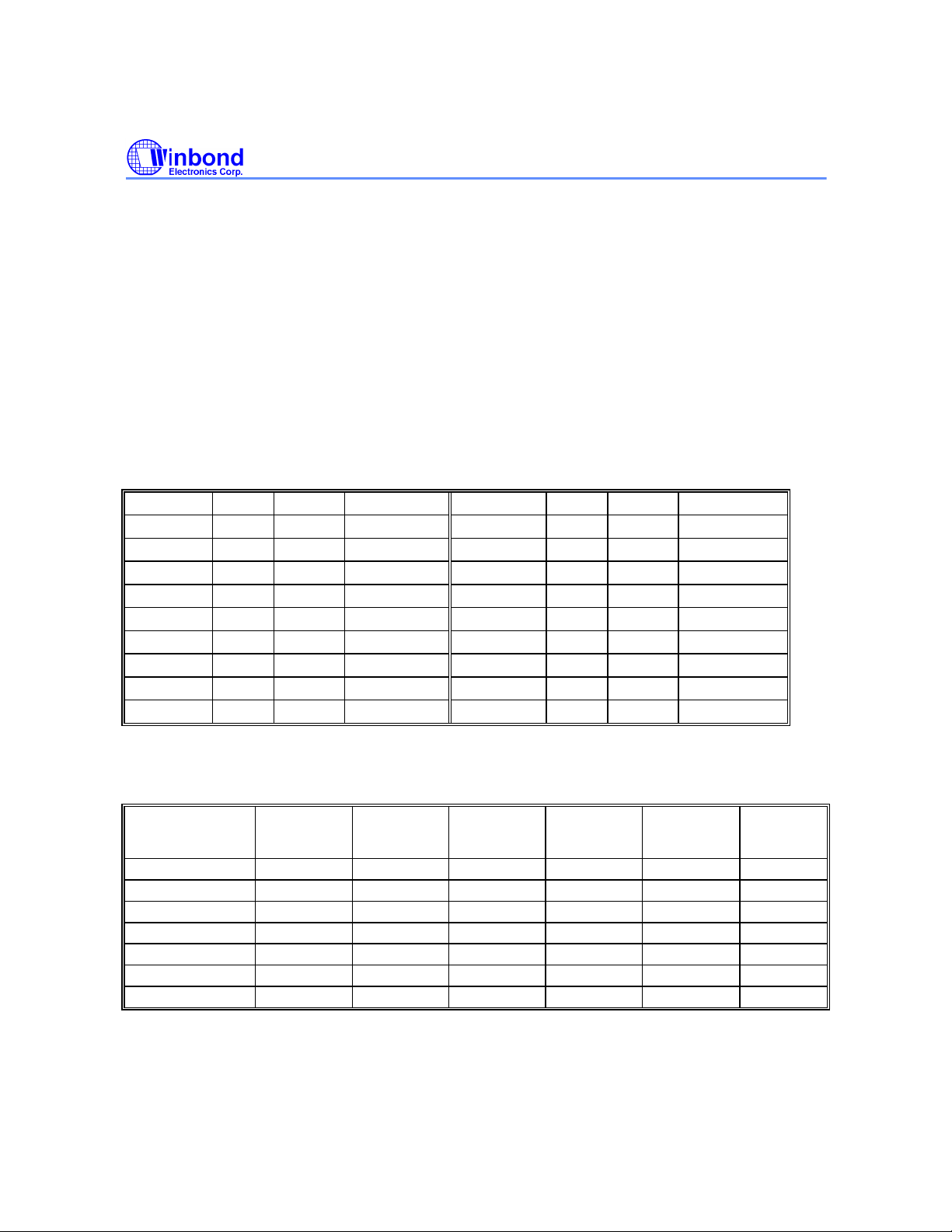
Table 2. Instructions that affect Flag settings
Instruction Carry Overflow Auxiliary Carry Instruction Carry Overflow Auxiliary Carry
ADD X X X CLR C 0
ADDC X X X CPL C X
SUBB X X X ANL C, bit X
MUL 0 X ANL C, bit X
DIV 0 X ORL C, bit X
DA A X ORL C, bit X
RRC A X MOV C, bit X
RLC A X CJNE X
SETB C 1
A "X" indicates that the modification is as per the result of instruction.
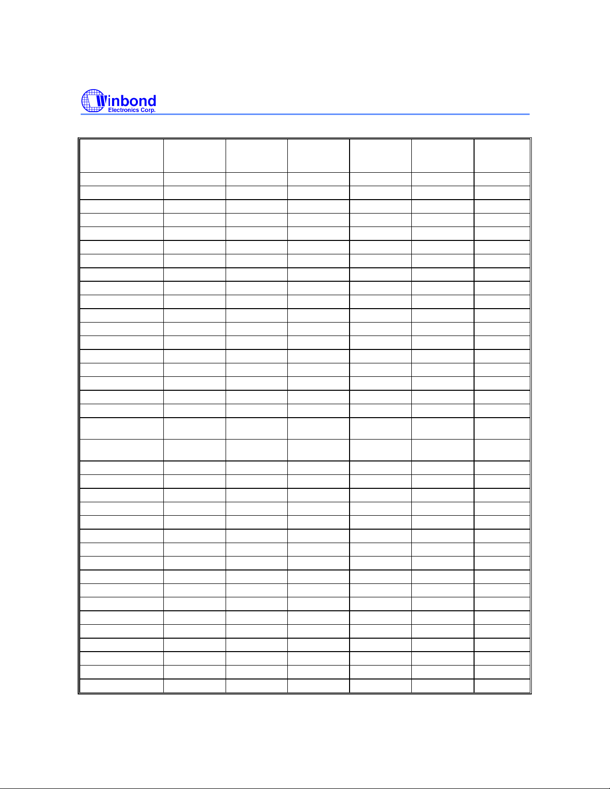
Table 3. Instruction Timing for W77C32
Instruction HEX
Op-Code
NOP 00 1 1 4 12 3
ADD A, R0 28 1 1 4 12 3
ADD A, R1 29 1 1 4 12 3
ADD A, R2 2A 1 1 4 12 3
ADD A, R3 2B 1 1 4 12 3
ADD A, R4 2C 1 1 4 12 3
ADD A, R5 2D 1 1 4 12 3
Bytes W77C32
Machine
Cycles
W77C32
Clock
Cycles
8032
Clock
Cycles
W77C32 vs.
8032 Speed
Publication Release Date: March 1999
- 25 - Revision A1
Ratio
Page 26
Preliminary W77C32
Table 3. Instruction Timing for W77C32, continued
Instruction HEX
Op-Code
ADD A, R6 2E 1 1 4 12 3
ADD A, R7 2F 1 1 4 12 3
ADD A, @R0 26 1 1 4 12 3
ADD A, @R1 27 1 1 4 12 3
ADD A, direct 25 2 2 8 12 1.5
ADD A, #data 24 2 2 8 12 1.5
ADDC A, R0 38 1 1 4 12 3
ADDC A, R1 39 1 1 4 12 3
ADDC A, R2 3A 1 1 4 12 3
ADDC A, R3 3B 1 1 4 12 3
ADDC A, R4 3C 1 1 4 12 3
ADDC A, R5 3D 1 1 4 12 3
ADDC A, R6 3E 1 1 4 12 3
ADDC A, R7 3F 1 1 4 12 3
ADDC A, @R0 36 1 1 4 12 3
ADDC A, @R1 37 1 1 4 12 3
ADDC A, direct 35 2 2 8 12 1.5
ADDC A, #data 34 2 2 8 12 1.5
ACALL addr11 71, 91, B1, 11,
31, 51, D1, F1
AJMP ADDR11 01, 21, 41, 61,
81, A1, C1, E1
ANL A, R0 58 1 1 4 12 3
ANL A, R1 59 1 1 4 12 3
ANL A, R2 5A 1 1 4 12 3
ANL A, R3 5B 1 1 4 12 3
ANL A, R4 5C 1 1 4 12 3
ANL A, R5 5D 1 1 4 12 3
ANL A, R6 5E 1 1 4 12 3
ANL A, R7 5F 1 1 4 12 3
ANL A, @R0 56 1 1 4 12 3
ANL A, @R1 57 1 1 4 12 3
ANL A, direct 55 2 2 8 12 1.5
ANL A, #data 54 2 2 8 12 1.5
ANL direct, A 52 2 2 8 12 1.5
ANL direct, #data 53 3 3 12 24 2
ANL C, bit 82 2 2 8 24 3
ANL C, /bit B0 2 2 8 24 3
CJNE A, direct, rel B5 3 4 16 24 1.5
Bytes W77C32
Machine
Cycles
2 3 12 24 2
2 3 12 24 2
W77C32
Clock
Cycles
8032
Clock
Cycles
W77C32 vs.
8032 Speed
Ratio
- 26 -
Page 27
Preliminary W77C32
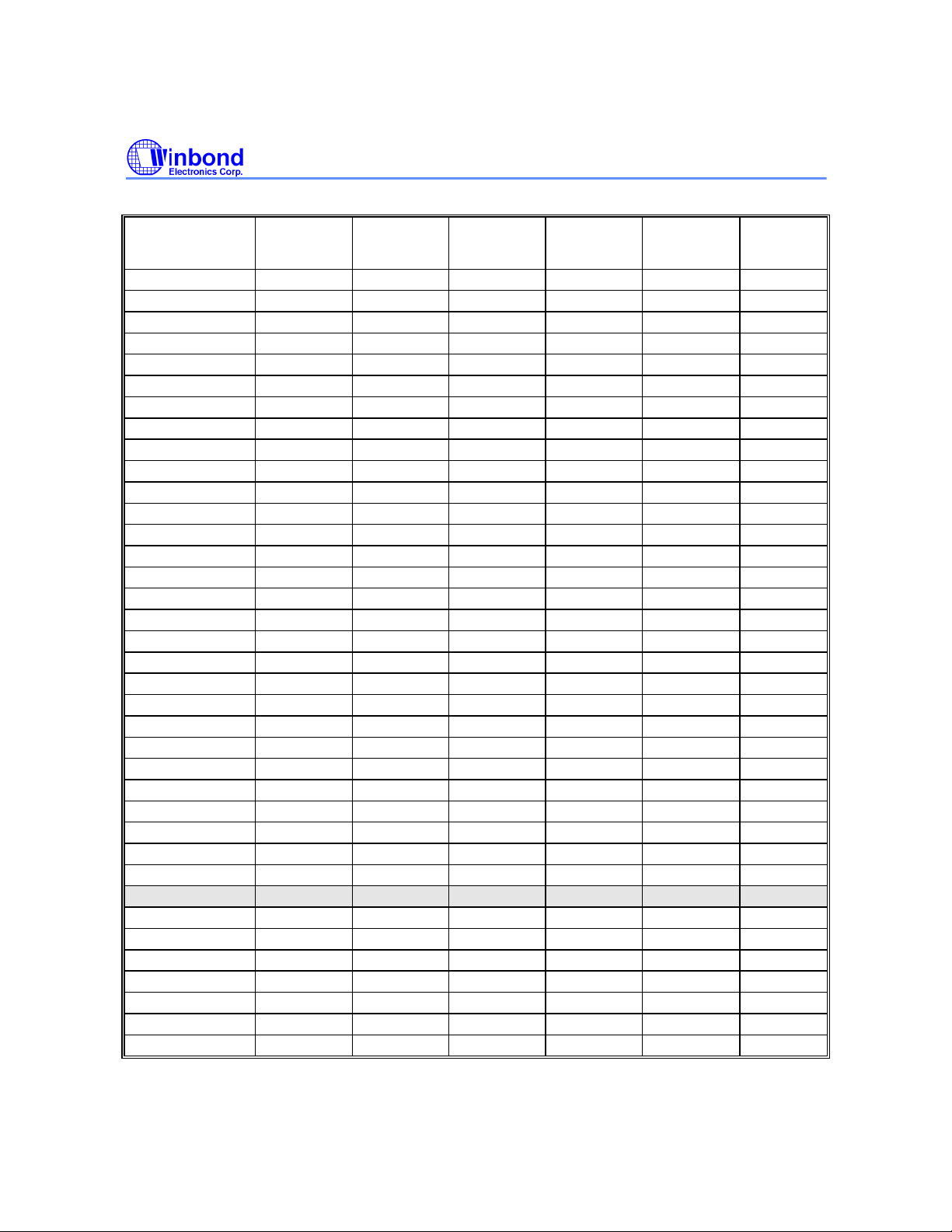
Table 3. Instruction Timing for W77C32, continued
Instruction HEX
Op-Code
CJNE A, #data, rel B4 3 4 16 24 1.5
CJNE @R0, #data, rel B6 3 4 16 24 1.5
CJNE @R1, #data, rel B7 3 4 16 24 1.5
CJNE R0, #data, rel B8 3 4 16 24 1.5
CJNE R1, #data, rel B9 3 4 16 24 1.5
CJNE R2, #data, rel BA 3 4 16 24 1.5
CJNE R3, #data, rel BB 3 4 16 24 1.5
CJNE R4, #data, rel BC 3 4 16 24 1.5
CJNE R5, #data, rel BD 3 4 16 24 1.5
CJNE R6, #data, rel BE 3 4 16 24 1.5
CJNE R7, #data, rel BF 3 4 16 24 1.5
CLR A E4 1 1 4 12 3
CPL A F4 1 1 4 12 3
CLR C C3 1 1 4 12 3
CLR bit C2 2 2 8 12 1.5
CPL C B3 1 1 4 12 3
CPL bit B2 2 2 8 12 1.5
DEC A 14 1 1 4 12 3
DEC R0 18 1 1 4 12 3
DEC R1 19 1 1 4 12 3
DEC R2 1A 1 1 4 12 3
DEC R3 1B 1 1 4 12 3
DEC R4 1C 1 1 4 12 3
DEC R5 1D 1 1 4 12 3
DEC R6 1E 1 1 4 12 3
DEC R7 1F 1 1 4 12 3
DEC @R0 16 1 1 4 12 3
DEC @R1 17 1 1 4 12 3
DEC direct 15 2 2 8 12 1.5
DEC DPTR A5 1 2 8 - DIV AB 84 1 5 20 48 2.4
DA A D4 1 1 4 12 3
DJNZ R0, rel D8 2 3 12 24 2
DJNZ R1, rel D9 2 3 12 24 2
DJNZ R5, rel DD 2 3 12 24 2
DJNZ R2, rel DA 2 3 12 24 2
DJNZ R3, rel DB 2 3 12 24 2
Bytes W77C32
Machine
Cycles
W77C32
Clock
Cycles
8032
Clock
Cycles
W77C32 vs.
8032 Speed
Ratio
Publication Release Date: March 1999
- 27 - Revision A1
Page 28
Preliminary W77C32
Table 3. Instruction Timing for W77C32, continued
Instruction HEX
Op-Code
DJNZ R4, rel DC 2 3 12 24 2
DJNZ R6, rel DE 2 3 12 24 2
DJNZ R7, rel DF 2 3 12 24 2
DJNZ direct, rel D5 3 4 16 24 1.5
INC A 04 1 1 4 12 3
INC R0 08 1 1 4 12 3
INC R1 09 1 1 4 12 3
INC R2 0A 1 1 4 12 3
INC R3 0B 1 1 4 12 3
INC R4 0C 1 1 4 12 3
INC R5 0D 1 1 4 12 3
INC R6 0E 1 1 4 12 3
INC R7 0F 1 1 4 12 3
INC @R0 06 1 1 4 12 3
INC @R1 07 1 1 4 12 3
INC direct 05 2 2 8 12 1.5
INC DPTR A3 1 2 8 24 3
JMP @A+DPTR 73 1 2 8 24 3
JZ rel 60 2 3 12 24 2
JNZ rel 70 2 3 12 24 2
JC rel 40 2 3 12 24 2
JNC rel 50 2 3 12 24 2
JB bit, rel 20 3 4 16 24 1.5
JNB bit, rel 30 3 4 16 24 1.5
JBC bit, rel 10 3 4 16 24 1.5
LCALL addr16 12 3 4 16 24 1.5
LJMP addr16 02 3 4 16 24 1.5
MUL AB A4 1 5 20 48 2.4
MOV A, R0 E8 1 1 4 12 3
MOV A, R1 E9 1 1 4 12 3
MOV A, R2 EA 1 1 4 12 3
MOV A, R3 EB 1 1 4 12 3
MOV A, R4 EC 1 1 4 12 3
MOV A, R5 ED 1 1 4 12 3
MOV A, R6 EE 1 1 4 12 3
MOV A, R7 EF 1 1 4 12 3
MOV A, @R0 E6 1 1 4 12 3
MOV A, @R1 E7 1 1 4 12 3
Bytes W77C32
Machine
Cycles
W77C32
Clock
Cycles
8032
Clock
Cycles
W77C32 vs.
8032 Speed
Ratio
- 28 -
Page 29
Preliminary W77C32
Table 3. Instruction Timing for W77C32, continued
Instruction HEX
Op-Code
MOV A, direct E5 2 2 8 12 1.5
MOV A, #data 74 2 2 8 12 1.5
MOV R0, A F8 1 1 4 12 3
MOV R1, A F9 1 1 4 12 3
MOV R2, A FA 1 1 4 12 3
MOV R3, A FB 1 1 4 12 3
MOV R4, A FC 1 1 4 12 3
MOV R5, A FD 1 1 4 12 3
MOV R6, A FE 1 1 4 12 3
MOV R7, A FF 1 1 4 12 3
MOV R0, direct A8 2 2 8 12 1.5
MOV R1, direct A9 2 2 8 12 1.5
MOV R2, direct AA 2 2 8 12 1.5
MOV R3, direct AB 2 2 8 12 1.5
MOV R4, direct AC 2 2 8 12 1.5
MOV R5, direct AD 2 2 8 12 1.5
MOV R6, direct AE 2 2 8 12 1.5
MOV R7, direct AF 2 2 8 12 1.5
MOV R0, #data 78 2 2 8 12 1.5
MOV R1, #data 79 2 2 8 12 1.5
MOV R2, #data 7A 2 2 8 12 1.5
MOV R3, #data 7B 2 2 8 12 1.5
MOV R4, #data 7C 2 2 8 12 1.5
MOV R5, #data 7D 2 2 8 12 1.5
MOV R6, #data 7E 2 2 8 12 1.5
MOV R7, #data 7F 2 2 8 12 1.5
MOV @R0, A F6 1 1 4 12 3
MOV @R1, A F7 1 1 4 12 3
MOV @R0, direct A6 2 2 8 12 1.5
MOV @R1, direct A7 2 2 8 12 1.5
MOV @R0, #data 76 2 2 8 12 1.5
MOV @R1, #data 77 2 2 8 12 1.5
MOV direct, A F5 2 2 8 12 1.5
MOV direct, R0 88 2 2 8 12 1.5
MOV direct, R1 89 2 2 8 12 1.5
MOV direct, R2 8A 2 2 8 12 1.5
MOV direct, R3 8B 2 2 8 12 1.5
Bytes W77C32
Machine
Cycles
W77C32
Clock
Cycles
8032
Clock
Cycles
W77C32 vs.
8032 Speed
Ratio
Publication Release Date: March 1999
- 29 - Revision A1
Page 30
Preliminary W77C32
Table 3. Instruction Timing for W77C32, continued
Instruction HEX
Op-Code
MOV direct, R4 8C 2 2 8 12 1.5
MOV direct, R5 8D 2 2 8 12 1.5
MOV direct, R6 8E 2 2 8 12 1.5
MOV direct, R7 8F 2 2 8 12 1.5
MOV direct, @R0 86 2 2 8 12 1.5
MOV direct, @R1 87 2 2 8 12 1.5
MOV direct, direct 85 3 3 12 24 2
MOV direct, #data 75 3 3 12 24 2
MOV DPTR, #data 16 90 3 3 12 24 2
MOVC A, @A+DPTR 93 1 2 8 24 3
MOVC A, @A+PC 83 1 2 8 24 3
MOVX A, @R0 E2 1 2 - 9 8 - 36 24 3 - 0.66
MOVX A, @R1 E3 1 2 - 9 8 - 36 24 3 - 0.66
MOVX A, @DPTR E0 1 2 - 9 8 - 36 24 3 - 0.66
MOVX @R0, A F2 1 2 - 9 8 - 36 24 3 - 0.66
MOVX @R1, A F3 1 2 - 9 8 - 36 24 3 - 0.66
MOVX @DPTR, A F0 1 2 - 9 8 - 36 24 3 - 0.66
MOV C, bit A2 2 2 8 12 1.5
MOV bit, C 92 2 2 8 24 3
ORL A, R0 48 1 1 4 12 3
ORL A, R1 49 1 1 4 12 3
ORL A, R2 4A 1 1 4 12 3
ORL A, R3 4B 1 1 4 12 3
ORL A, R4 4C 1 1 4 12 3
ORL A, R5 4D 1 1 4 12 3
ORL A, R6 4E 1 1 4 12 3
ORL A, R7 4F 1 1 4 12 3
ORL A, @R0 46 1 1 4 12 3
ORL A, @R1 47 1 1 4 12 3
ORL A, direct 45 2 2 8 12 1.5
ORL A, #data 44 2 2 8 12 1.5
ORL direct, A 42 2 2 8 12 1.5
ORL direct, #data 43 3 3 12 24 2
ORL C, bit 72 2 2 8 24 3
ORL C, /bit A0 2 2 6 24 3
PUSH direct C0 2 2 8 24 3
POP direct D0 2 2 8 24 3
RET 22 1 2 8 24 3
Bytes W77C32
Machine
Cycles
W77C32
Clock
Cycles
8032
Clock
Cycles
W77C32 vs.
8032 Speed
Ratio
- 30 -
Page 31
Preliminary W77C32
Table 3. Instruction Timing for W77C32, continued
Instruction HEX
Op-Code
RETI 32 1 2 8 24 3
RL A 23 1 1 4 12 3
RLC A 33 1 1 4 12 3
RR A 03 1 1 4 12 3
RRC A 13 1 1 4 12 3
SETB C D3 1 1 4 12 3
SETB bit D2 2 2 8 12 1.5
SWAP A C4 1 1 4 12 3
SJMP rel 80 2 3 12 24 2
SUBB A, R0 98 1 1 4 12 3
SUBB A, R1 99 1 1 4 12 3
SUBB A, R2 9A 1 1 4 12 3
SUBB A, R3 9B 1 1 4 12 3
SUBB A, R4 9C 1 1 4 12 3
SUBB A, R5 9D 1 1 4 12 3
SUBB A, R6 9E 1 1 4 12 3
SUBB A, R7 9F 1 1 4 12 3
SUBB A, @R0 96 1 1 4 12 3
SUBB A, @R1 97 1 1 4 12 3
SUBB A, direct 95 2 2 8 12 1.5
SUBB A, #data 94 2 2 8 12 1.5
XCH A, R0 C8 1 1 4 12 3
XCH A, R1 C9 1 1 4 12 3
XCH A, R2 CA 1 1 4 12 3
XCH A, R3 CB 1 1 4 12 3
XCH A, R4 CC 1 1 4 12 3
XCH A, R5 CD 1 1 4 12 3
XCH A, R6 CE 1 1 4 12 3
XCH A, R7 CF 1 1 4 12 3
XCH A, @R0 C6 1 1 4 12 3
XCH A, @R1 C7 1 1 4 12 3
XCHD A, @R0 D6 1 1 4 12 3
XCHD A, @R1 D7 1 1 4 12 3
XCH A, direct C5 2 2 8 12 1.5
XRL A, R0 68 1 1 4 12 3
XRL A, R1 69 1 1 4 12 3
XRL A, R2 6A 1 1 4 12 3
Bytes W77C32
Machine
Cycles
W77C32
Clock
Cycles
8032
Clock
Cycles
W77C32 vs.
8032 Speed
Ratio
Publication Release Date: March 1999
- 31 - Revision A1
Page 32
Preliminary W77C32
WR
Table 3. Instruction Timing for W77C32, continued
Instruction HEX
Op-Code
XRL A, R3 6B 1 1 4 12 3
XRL A, R4 6C 1 1 4 12 3
XRL A, R5 6D 1 1 4 12 3
XRL A, R6 6E 1 1 4 12 3
XRL A, R7 6F 1 1 4 12 3
XRL A, @R0 66 1 1 4 12 3
XRL A, @R1 67 1 1 4 12 3
XRL A, direct 65 2 2 8 12 1.5
XRL A, #data 64 2 2 8 12 1.5
XRL direct, A 62 2 2 8 12 1.5
XRL direct, #data 63 3 3 12 24 2
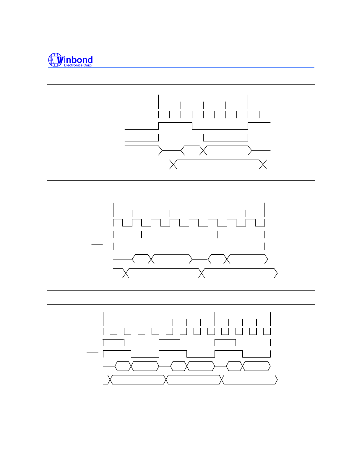
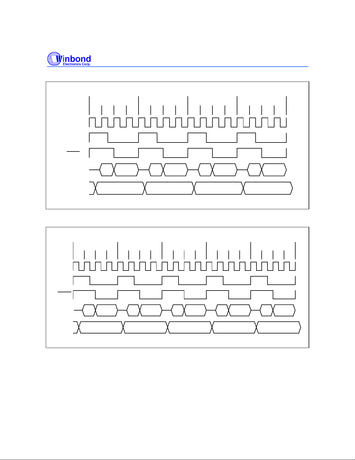
INSTRUCTION TIMING
The instruction timing for the W77C32 is an important aspect, especially for those users who wish to
use software instructions to generate timing delays. Also, it provides the user with an insight into the
timing differences between the W77C32 and the standard 8032. In the W77C32 each machine cycle
is four clock periods long. Each clock period is designated a state. Thus each machine cycle is made
up of four states, C1, C2, C3 and C4 in that order. Due to the reduced time for each instruction
execution, both the clock edges are used for internal timing. Hence it is important that the duty cycle
of the clock be as close to 50% as possible to avoid timing conflicts. As mentioned earlier, the
W77C32 does one op-code fetch per machine cycle. Therefore, in most of the instructions, the
number of machine cycles needed to execute the instruction is equal to the number of bytes in the
instruction. Of the 256 available op-codes, 128 of them are single cycle instructions. Thus more than
half of all op-codes in the W77C32 are executed in just four clock periods. Most of the two-cycle
instructions are those that have two byte instruction codes. However there are some instructions that
have only one byte instructions, yet they are two cycle instructions. One instruction which is of
importance is the MOVX instruction. In the standard 8032, the MOVX instruction is always two
machine cycles long. However in the W77C32, the user has a facility to stretch the duration of this
instruction from 2 machine cycles to 9 machine cycles. The RD and
proportionately elongated. This gives the user flexibility in accessing both fast and slow peripherals
without the use of external circuitry and with minimum software overhead. The rest of the instructions
are either three, four or five machine cycle instructions. Note that in the W77C32, based on the
number of machine cycles, there are five different types, while in the standard 8032 there are only
three. However, in the W77C32 each machine cycle is made of only 4 clock periods compared to the
12 clock periods for the standard 8032. Therefore, even though the number of categories has
increased, each instruction is at least 1.5 to 3 times faster than the standard 8032 in terms of clock
periods.
Bytes W77C32
Machine
Cycles
W77C32
Clock
Cycles
8032
Clock
Cycles
W77C32 vs.
8032 Speed
Ratio
strobe lines are also
- 32 -
Page 33
CLK
ALE
PSEN
AD7-0
C1
Single Cycle
C2
A7-0
Preliminary W77C32
C3
Data_ in D7-0
C4
CLK
ALE
PSEN
AD7-0
PORT 2
CLK
PORT 2
Address A15-8
Figure 3: Single Cycle Instruction Timing
Instruction Fetch
C4C3C2C1
PC
OP-CODE
Address A15-8
Figure 4: Two Cycle Instruction Timing
Operand Fetch
C3C2C1
Address A15-8
Operand FetchOperand FetchInstruction Fetch
C2 C3 C4C2 C3 C4C4C3C2 C1C1C1
C4
OPERANDPC+1
ALE
PSEN
AD7-0
PORT 2
OPERANDOPERAND A7-0A7-0 A7-0OP-CODE
Address A15-8Address A15-8Address A15-8
Figure 5: Three Cycle Instruction Timing
Publication Release Date: March 1999
- 33 - Revision A1
Page 34
CLK
ALE
PSEN
Preliminary W77C32
Operand FetchOperand FetchOperand FetchInstruction Fetch
C4C3 C2C1 C4C3 C2C1 C4C3
C2C1 C4C3C2C1
AD7-0
CLK
ALE
PSEN
AD7-0
PORT 2
Port 2
OP-CODE
A7-0
C4C3 C2C1 C4C3 C2C1 C4C3 C2C1 C4C3
OP-CODE
C2C1 C4C3C2C1
A7-0
Figure 6: Four Cycle Instruction Timing
Operand FetchOperand FetchInstruction Fetch
OPERANDOPERAND
Operand Fetch
OPERANDOPERANDOPERAND
A7-0A7-0A7-0A7-0
Address A15-8Address A15-8Address A15-8Address A15-8
A7-0A7-0
OPERAND
Address A15-8Address A15-8Address A15-8Address A15-8
Operand Fetch
OPERAND
A7-0
Address A15-8
Figure 7: Five Cycle Instruction Timing
- 34 -
Page 35

Preliminary W77C32
MOVX Instruction
The W77C32, like the standard 8032, uses the MOVX instruction to access external Data Memory.
This Data Memory includes both off-chip memory as well as memory mapped peripherals. While the
results of the MOVX instruction are the same as in the standard 8032, the operation and the timing of
the strobe signals have been modified in order to give the user much greater flexibility.
The MOVX instruction is of two types, the MOVX @Ri and MOVX @DPTR. In the MOVX @Ri, the
address of the external data comes from two sources. The lower 8-bits of the address are stored in
the Ri register of the selected working register bank. The upper 8-bits of the address come from the
port 2 SFR. In the MOVX @DPTR type, the full 16-bit address is supplied by the Data Pointer.
Since the W77C32 has two Data Pointers, DPTR and DPTR1, the user has to select between the two
by setting or clearing the DPS bit. The Data Pointer Select bit (DPS) is the LSB of the DPS SFR,
which exists at location 86h. No other bits in this SFR have any effect, and they are set to 0. When
DPS is 0, then DPTR is selected, and when set to 1, DPTR1 is selected. The user can switch between
DPTR and DPTR1 by toggling the DPS bit. The quickest way to do this is by the INC instruction. The
advantage of having two Data Pointers is most obvious while performing block move operations. The
accompanying code shows how the use of two separate Data Pointers speeds up the execution time
for code performing the same task.
Block Move with single Data Pointer:
; SH and SL are the high and low bytes of Source Address
; DH and DL are the high and low bytes of Destination Address
; CNT is the number of bytes to be moved
Machine cycles of W77C32
#
MOV R2, #CNT ; Load R2 with the count value 2
MOV R3, #SL ; Save low byte of Source Address in R3 2
MOV R4, #SH ; Save high byte of Source address in R4 2
MOV R5, #DL ; Save low byte of Destination Address in R5 2
MOV R6, #DH ; Save high byte of Destination address in R6 2
LOOP:
MOV DPL, R3 ; Load DPL with low byte of Source address 2
MOV DPH, R4 ; Load DPH with high byte of Source address 2
MOVX A, @DPTR ; Get byte from Source to Accumulator 2
INC DPTR ; Increment Source Address to next byte 2
MOV R3, DPL ; Save low byte of Source address in R3 2
MOV R4, DPH ; Save high byte of Source Address in R4 2
MOV DPL, R5 ; Load low byte of Destination Address in DPL 2
MOV DPH, R6 ; Load high byte of Destination Address in DPH 2
MOVX @DPTR, A ; Write data to destination 2
INC DPTR ; Increment Destination Address 2
MOV DPL, R5 ; Save low byte of new destination address in R5 2
MOV DPH, R6 ; Save high byte of new destination address in R6 2
DJNZ R2, LOOP ; Decrement count and do LOOP again if count <> 0 2
Publication Release Date: March 1999
- 35 - Revision A1
Page 36

Preliminary W77C32
Machine cycles in standard 8032 = 10 + (26 * CNT)
Machine cycles in W77C32 = 10 + (26 * CNT)
If CNT = 50
Clock cycles in standard 8032= ((10 + (26 *50)) * 12 = (10 + 1300) * 12 = 15720
Clock cycles in W77C32 = ((10 + (26 * 50)) * 4 = (10 + 1300) * 4 = 5240
Block Move with Two Data Pointers in W77C32:
; SH and SL are the high and low bytes of Source Address
; DH and DL are the high and low bytes of Destination Address
; CNT is the number of bytes to be moved
Machine cycles of W77C32
#
MOV R2, #CNT ; Load R2 with the count value 2
MOV DPS, #00h ; Clear DPS to point to DPTR 2
MOV DPTR, #DHDL ; Load DPTR with Destination address 3
INC DPS ; Set DPS to point to DPTR1 2
MOV DPTR, #SHSL ; Load DPTR1 with Source address 3
LOOP:
MOVX A, @DPTR ; Get data from Source block 2
INC DPTR ; Increment source address 2
DEC DPS ; Clear DPS to point to DPTR 2
MOVX @DPTR, A ; Write data to Destination 2
INC DPTR ; Increment destination address 2
INC DPS ; Set DPS to point to DPTR1 2
DJNZ R2, LOOP ; Check if all done 3
Machine cycles in W77C32 = 12 + (15 * CNT)
If CNT = 50
Clock cycles in W77C32 = (12 + (15 * 50)) * 4 = (12 + 750) * 4 = 3048
We can see that in the first program the standard 8032 takes 15720 cycles, while the W77C32 takes
only 5240 cycles for the same code. In the second program, written for the W77C32, program
execution requires only 3048 clock cycles. If the size of the block is increased then the saving is even
greater.
External Data Memory Access Timing
The timing for the MOVX instruction is another feature of the W77C32. In the standard 8032, the
MOVX instruction has a fixed execution time of 2 machine cycles. However in the W77C32, the
duration of the access can be varied by the user.
The instruction starts off as a normal op-code fetch of 4 clocks. In the next machine cycle, the
W77C32 puts out the address of the external Data Memory and the actual access occurs here. The
user can change the duration of this access time by setting the STRETCH value. The Clock Control
SFR (CKCON) has three bits that control the stretch value. These three bits are M2-0 (bits 2-0 of
CKCON). These three bits give the user 8 different access time options. The stretch can be varied
from 0 to 7, resulting in MOVX instructions that last from 2 to 9 machine cycles in length. Note that
- 36 -
Page 37
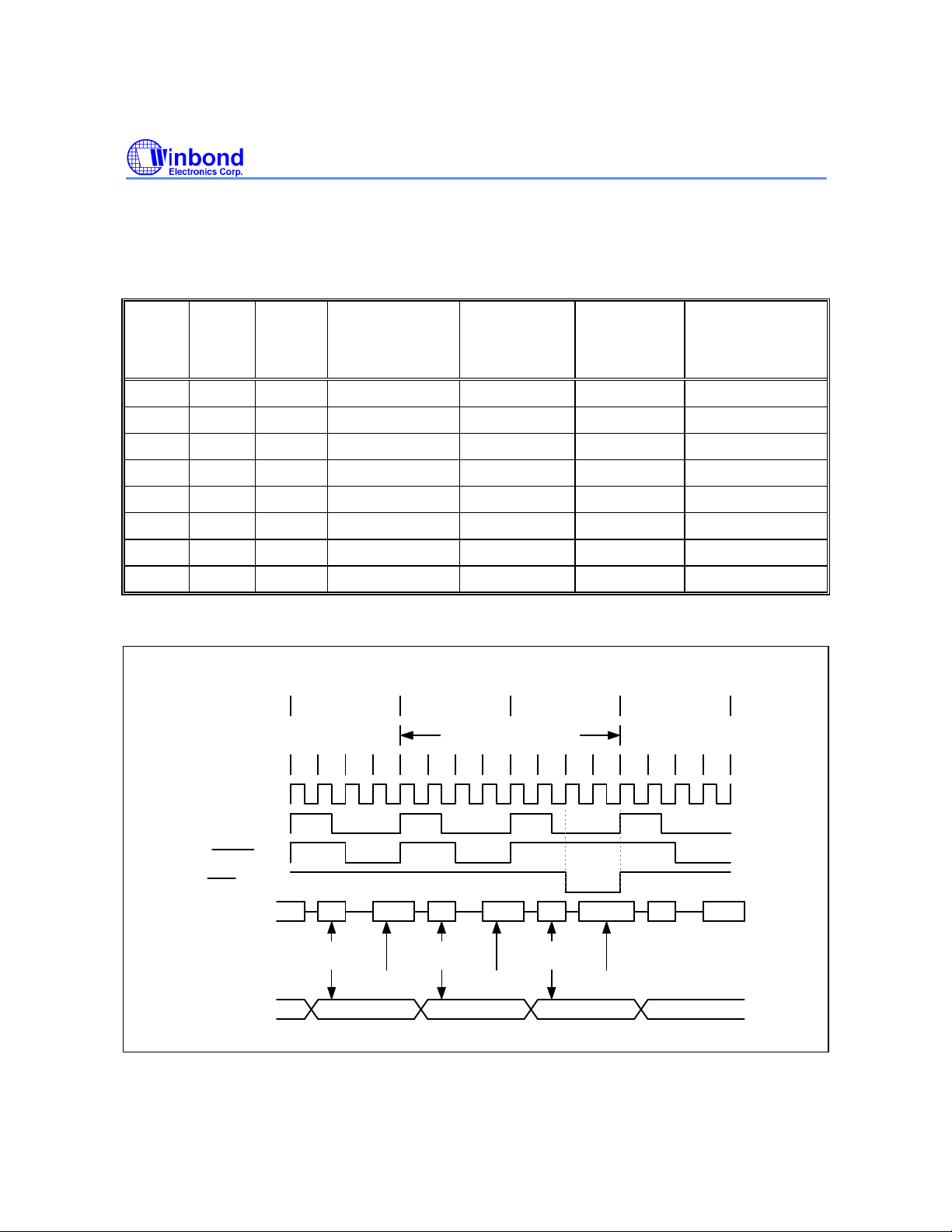
Preliminary W77C32
the stretching of the instruction only results in the elongation of the MOVX instruction, as if the state
of the CPU was held for the desired period. There is no effect on any other instruction or its timing. By
default, the Stretch value is set at 1, giving a MOVX instruction of 3 machine cycles. If desired by the
user the stretch value can be set to 0 to give the fastest MOVX instruction of only 2 machine cycles.
Table 4. Data Memory Cycle Stretch Values
M2 M1 M0 Machine
Cycles
/RD or /WR
strobe width
in Clocks
/RD or /WR
strobe width
@25 MHz
/RD or /WR
strobe width
@40 MHz
0 0 0 2 2 80 nS 50 nS
0 0 1 3(default) 4 160 nS 100 nS
0 1 0 4 8 320 nS 200 nS
0 1 1 5 12 480 nS 300 nS
1 0 0 6 16 640 nS 400 nS
1 0 1 7 20 800 nS 500 nS
1 1 0 8 24 960 nS 600 nS
1 1 1 9 28 1120 nS 700 nS
Last Cycle
of Previous
Instruction
First
Machine cycle
MOVX instruction cycle
Second
Machine cycle
Next Instruction
Machine Cycle
CLK
ALE
PSEN
WR
PORT 0
PORT 2
C4
C1 C4C3C2C1 C4C3C2C1 C4C3C2C1
MOVX Inst.
C3C2
A0-A7
Address
D0-D7
Next Inst.
Address
MOVX Inst.
Figure 8: Data Memory Write with Stretch Value = 0
D0-D7A0-A7
MOVX Data
Address
Next Inst. Read
A0-A7
MOVX Data out
A15-A8A15-A8A15-A8
D0-D7
Publication Release Date: March 1999
- 37 - Revision A1
A0-A7
D0-D7
A15-A8
Page 38
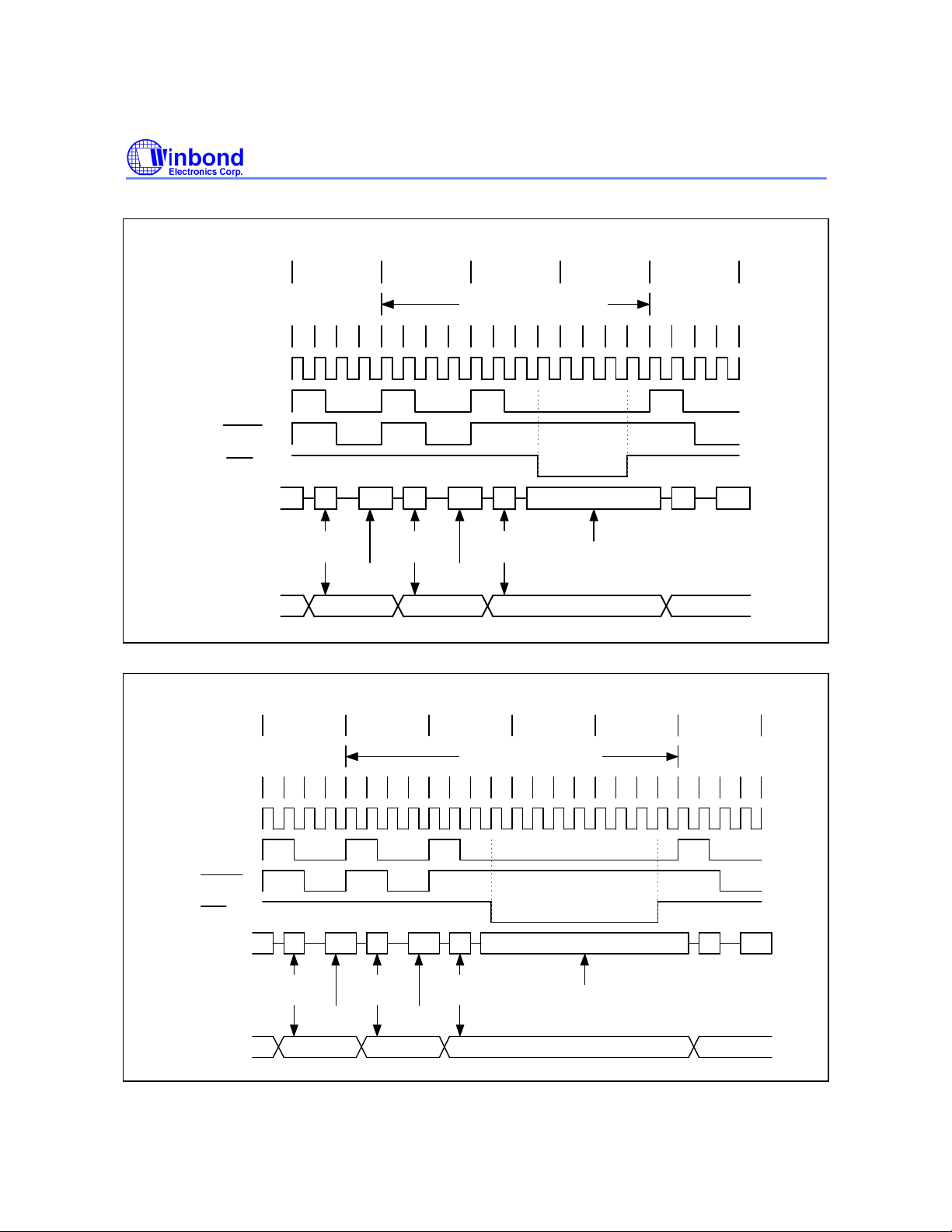
Preliminary W77C32
CLK
ALE
PSEN
WR
PORT 0
PORT 2
Last Cycle
of Previous
First
Machine Cycle
Second
Machine Cycle
Instruction
MOVX instruction cycle
C4
C3C2
C1 C4C3C2C1 C4C3C2C1 C4C3C2C1
A0-A7
MOVX Inst.
Address
MOVX Inst.
D0-D7
A0-A7
Next Inst.
Address
D0-D7
MOVX Data
Next Inst.
Read
Address
Figure 9: Dada Memory Write with Stretch Value = 1
Third
Machine Cycle
MOVX Data out
Next Instruction
Machine Cycle
C4C3C2C1
A0-A7D0-D7A0-A7
D0-D7
A15-A8A15-A8A15-A8A15-A8
CLK
ALE
PSEN
WR
PORT 0
PORT 2
Last Cycle
of Previous
First
Machine Cycle
Second
Machine Cycle
Instruction
MOVX instruction cycle
C4
C3C2
C1 C4C3C2C1 C4C3C2C1 C4C3C2C1
A0-A7
MOVX Inst.
Address
D0-D7
Next Inst.
MOVX Inst.
A0-A7
Address
Next Inst.
D0-D7
Read
A0-A7
MOVX Data
Address
Figure 10: Dada Memory Write with Stretch Value = 2
- 38 -
Third
Machine Cycle
D0-D7
MOVX Data out
Fourth
Machine Cycle
Instruction
Machine Cycle
C4C3C2C1 C4C3C2C1
A0-A7
Next
D0-D7
A15-A8A15-A8A15-A8A15-A8
Page 39
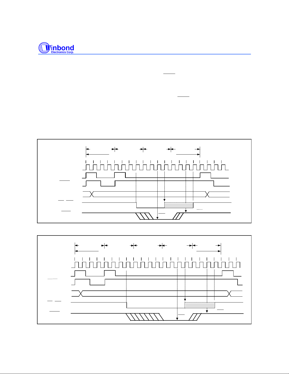
Preliminary W77C32
WAIT
WAIT
Wait State Control Signal
Either with the software using stretch value to change the required machine cycle of MOVX
instruction, the W77C32 provides another hardware signal
external data access timing. This wait state control signal is the alternate function of P4.0 such that it
can only be invoked to 44-pin PLCC/QFP package type. The wait state control signal can be enabled
by setting WS (ROMMAP.7) bit. When enabled, the setting of stretch value decides the minimum
length of MOVX instruction cycle and the device will sample the
the rising edge of read/write strobe signal during MOVX instruction. Once this signal being
recongnized, one more machine cycle (wait state cycle) will be inserted into next cycle. The inserted
wait state cycles are unlimited, so the MOVX instruction cycle will end in which the wait state control
signal is deactivated. Using wait state control signal allows a dynamically access timimg to a selected
external peripheral. The WS bit is accessed by the Timed Access Protection procedure.
Wait State Control Signal Timing ( when Stretch = 1 )
to implement the wider duration of
pin at each C3 state before
First
Machine
Cycle
Second
Machine
Cycle
Machine
MOVX Instruction
CLOCK
C2 C3 C4C1
C2 C3 C4C1 C2 C3 C4C1
ALE
PSEN
ADDRESS
RD / WR
WAIT
Wait State Control Signal Timing ( when Stretch = 2 )
Third
Machine
Cycle
MOVX Instruction
CLOCK
ALE
PSEN
First
Machine
Cycle
C2 C3 C4C1
Second
Machine
Cycle
C2 C3 C4C1 C2 C3 C4C1
Third
Cycle
sample
WAIT
original rising edge
Extended duration
Fourth
Machine
Cycle
C2 C3 C4C1
Wait-State
Cycle
C2 C3 C4C1
sample WAIT
Wait-State
Cycle
C2 C3 C4C1
C3 C4C2C1
C2C1
ADDRESS
RD / WR
WAIT
original rising edge
Extended duration
sample
WAIT
sample WAIT
Publication Release Date: March 1999
- 39 - Revision A1
Page 40

Preliminary W77C32
PSEN
POWER MANAGEMENT
The W77C32 has several features that help the user to modify the power consumption of the device.
The power saving features are basically the POWER DOWN mode, ECONOMY mode and the IDLE
mode of operation.
Idle Mode
The user can put the device into idle mode by writing 1 to the bit PCON.0. The instruction that sets
the idle bit is the last instruction that will be executed before the device goes into Idle Mode. In the
Idle mode, the clock to the CPU is halted, but not to the Interrupt, Timer, Watchdog timer and Serial
port blocks. This forces the CPU state to be frozen; the Program counter, the Stack Pointer, the
Program Status Word, the Accumulator and the other registers hold their contents. The ALE and
pins are held high during the Idle state. The port pins hold the logical states they had at the
time Idle was activated. The Idle mode can be terminated in two ways. Since the interrupt controller is
still active, the activation of any enabled interrupt can wake up the processor. This will automatically
clear the Idle bit, terminate the Idle mode, and the Interrupt Service Routine (ISR) will be executed.
After the ISR, execution of the program will continue from the instruction which put the device into
Idle mode.
The Idle mode can also be exited by activating the reset. The device can be put into reset either by
applying a high on the external RST pin, a Power on/fail reset condition or a Watchdog timer reset.
The external reset pin has to be held high for at least two machine cycles I.e. 8 clock periods to be
recognized as a valid reset. In the reset condition the program counter is reset to 0000h and all the
SFRs are set to the reset condition. Since the clock is already running there is no delay and execution
starts immediately. In the Idle mode, the Watchdog timer continues to run, and if enabled, a time-out
will cause a watchdog timer interrupt which will wake up the device. The software must reset the
Watchdog timer in order to preempt the reset which will occur after 512 clock periods of the time-out.
When the W77C32 is exiting from an Idle mode with a reset, the instruction following the one which
put the device into Idle mode is not executed. So there is no danger of unexpected writes.
Economy Mode
The power consumption of microcontroller relates to operating frequency. The W77C32 offers a
Economy mode to reduce the internal clock rate dynamically without external components. By
default, one machine cycle needs 4 clocks. In Economy mode, software can select 4, 64 or 1024
clocks per machine cycle. It keeps the CPU operating at a acceptable speed but eliminates the power
consumption. In the Idle mode, the clock of the core logic is stopped, b+ut all clocked peripherals
such as watchdog timer are still running at a rate of clock/4. In the Economy mode, all clocked
peripherals run at the same reduced clocks rate as in core logic. So the Economy mode may provide
a lower power consumption than idle mode.
Software invokes the Economy mode by setting the appropriate bits in the SFRs. Setting the bits
CD0(PMR.6),CD1(PMR.7) decides the instruction cycle rate as below:
CD1 CD0 clocks/machine cycle
0 0 Reserved
0 1 4 (default)
1 0 64
1 1 1024
- 40 -
Page 41

Preliminary W77C32
PSEN
The selection of instruction rate is going to take effect after a delay of one instruction cycle. Switching
to divide by 64 or 1024 mode must first go from divide by 4 mode. This means software can not
switch directly between clock/64 and clock/1024 mode. The CPU has to return clock/4 mode first,
then go to clock/64 or clock/1024 mode.
The W77C32 allows the user to use internal RC oscillator instead of external crystal. Setting the
XT/RG bit (EXIF.3) selects the crystal or RC oscillator as the clock source. When invoking RC
oscillator in Economy mode, software may set the XTOFF bit to turn off the crystal amplifier for
saving power. The CPU would run at the clock rate of approximately 2−4 MHz divided by 4, 64 or
1024. The RC oscillator is not precise so that can not be invoked to the operation which needs the
accurate time-base such as serial communication. The RGMD(EXIF.2) indicates current clock source.
When switching the clock source, CPU needs one instruction cycle delay to take effect new setting. If
crystal amplifier is disabled and RC oscillator is present clock source, software must first clear the
XTOFF bit to turn on crystal amplifier before switch to crystal operation. Hardware will set the XTUP
bit (STATUS.4) once the crystal is warm-up and ready for use. It is unable to set XT/ RG bit to 1 if
XTUP = 0.
In Economy mode, the serial port can not receive/transmit data correctly because the baud rate is
changed. In some systems, the external interrupts may require the fastest process such that the
reducing of operating speed is restricted. In order to solve these dilemmas, the W77C32 offers a
switchback feature which allows the CPU back to clock/4 mode immediately when triggered by serial
operation or external interrupts. The switchback feature is enabled by setting the SWB bit (PMR.5). A
serial port reception/transmission or qualified external interrupt which is enabled and acknowledged
without block conditions will cause CPU to return to divide by 4 mode. For the serial port reception, a
switchback is generated by a falling edge associated with start bit if the serial port reception is
enabled. When a serial port transmission, an instruction which writes a byte of data to serial port
buffer will cause a switchback to ensure the correct transmission. The switchback feature is
unaffected by serial port interrupt flags. After a switchback is generated, the software can manually
return the CPU to Economy mode. Note that the modification of clock control bits CD0 and CD1 will
be ignored during serial port transmit/receive when switchback is enabled. The Watchdog timer reset,
power-on/fail reset or external reset will force the CPU to return to divide by 4 mode.
Power Down Mode
The device can be put into Power Down mode by writing 1 to bit PCON.1. The instruction that does
this will be the last instruction to be executed before the device goes into Power Down mode. In the
Power Down mode, all the clocks are stopped and the device comes to a halt. All activity is
completely stopped and the power consumption is reduced to the lowest possible value. In this state
the ALE and
SFRs.
The W77C32 will exit the Power Down mode with a reset or by an external interrupt pin enabled as
level detect. An external reset can be used to exit the Power down state. The high on RST pin
terminates the Power Down mode, and restarts the clock. The program execution will restart from
0000h. In the Power down mode, the clock is stopped, so the Watchdog timer cannot be used to
provide the reset to exit Power down mode.
The W77C32 can be woken from the Power Down mode by forcing an external interrupt pin activated,
provided the corresponding interrupt is enabled, while the global enable(EA) bit is set and the external
input has been set to a level detect mode. If these conditions are met, then the low level on the
external pin re-starts the oscillator. Then device executes the interrupt service routine for the
corresponding external interrupt. After the interrupt service routine is completed, the program
pins are pulled low. The port pins output the values held by their respective
Publication Release Date: March 1999
- 41 - Revision A1
Page 42
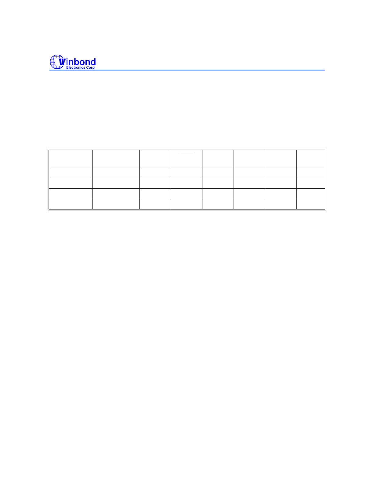
Preliminary W77C32
PSEN
execution returns to the instruction after the one which put the device into Power Down mode and
continues from there. When RGSL(EXIF.1) bit is set to 1, the CPU will use the internal RC oscillator
instead of crystal to exit Power Down mode. The microcontroller will automatically switch from RC
oscillator to crystal after clock is stable. The RC oscillator runs at approximately 2−4 MHz. Using RC
oscillator to exit from Power Down mode saves the time for waiting crystal start-up. It is useful in the
low power system which usually be awakened from a short operation then returns to Power Down
mode.
Table 5. Status of external pins during Idle and Power Down
MODE PROGRAM
MEMORY
Idle Internal 1 1 Data Data Data Data
Idle External 1 1 Float Data Address Data
Power Down Internal 0 0 Data Data Data Data
Power Down External 0 0 Float Data Data Data
ALE
PORT0 PORT1 PORT2 PORT3
RESET CONDITIONS
The user has several hardware related options for placing the W77C32 into reset condition. In
general, most register bits go to their reset value irrespective of the reset condition, but there are a
few flags whose state depends on the source of reset. The user can use these flags to determine the
cause of reset using software. There are three ways of putting the device into reset state. They are
External reset, Power on/fail reset and Watchdog reset.
External Reset
The device continuously samples the RST pin at state C4 of every machine cycle. Therefore the RST
pin must be held for at least 2 machine cycles to ensure detection of a valid RST high. The reset
circuitry then synchronously applies the internal reset signal. Thus the reset is a synchronous
operation and requires the clock to be running to cause an external reset.
Once the device is in reset condition, it will remain so as long as RST is 1. Even after RST is
deactivated, the device will continue to be in reset state for up to two machine cycles, and then begin
program execution from 0000h. There is no flag associated with the external reset condition. However
since the other two reset sources have flags, the external reset can be considered as the default reset
if those two flags are cleared.
Watchdog Timer Reset
The Watchdog timer is a free running timer with programmable time-out intervals. The user can clear
the watchdog timer at any time, causing it to restart the count. When the time-out interval is reached
an interrupt flag is set. If the Watchdog reset is enabled and the watchdog timer is not cleared, then
512 clocks from the flag being set, the watchdog timer will generate a reset . This places the device
into the reset condition. The reset condition is maintained by hardware for two machine cycles. Once
the reset is removed the device will begin execution from 0000h.
RESET STATE
Most of the SFRs and registers on the device will go to the same condition in the reset state. The
Program Counter is forced to 0000h and is held there as long as the reset condition is applied.
- 42 -
Page 43

Preliminary W77C32
However, the reset state does not affect the on-chip RAM. The data in the RAM will be preserved
during the reset. However, the stack pointer is reset to 07h, and therefore the stack contents will be
lost. The RAM contents will be lost if the VDD falls below approximately 2V, as this is the minimum
voltage level required for the RAM to operate normally. Therefore after a first time power on reset the
RAM contents will be indeterminate. During a power fail condition, if the power falls below 2V, the
RAM contents are lost. Hence it should be assumed that after a power on/fail reset, POR = 1, the
RAM contents are lost.
After a reset most SFRs are cleared. Interrupts and Timers are disabled. The Watchdog timer is
disabled if the reset source was a POR. The port SFRs have FFh written into them which puts the
port pins in a high state. Port 0 floats as it does not have on-chip pull-ups.
Table 6. SFR Reset Value
SFR NAME RESET VALUE SFR NAME RESET VALUE
P0 11111111b IE 00000000b
SP 00000111b SADDR 00000000b
DPL 00000000b P3 11111111b
DPH 00000000b IP x0000000b
DPL1 00000000b SADEN 00000000b
DPH1 00000000b T2CON 00000000b
DPS 00000000b T2MOD 00000x00b
PCON 00xx0000b RCAP2L 00000000b
TCON 00000000b RCAP2H 00000000b
TMOD 00000000b TL2 00000000b
TL0 00000000b TH2 00000000b
TL1 00000000b TA 11111111b
TH0 00000000b PSW 00000000b
TH1 00000000b WDCON 0x0x0xx0b
CKCON 00000001b ACC 00000000b
P1 11111111b EIE
SCON 00000000b B 00000000b
SBUF
P2 11111111b PC 00000000b
SADDR1 00000000b SADEN1 00000000b
SCON1 00000000b SBUF1
ROMMAP
EXIF
P4
xxxxxxxxb
01xxxxxxb
0000xxx0b
xxxx1111b
EIP xxx00000b
PMR 010xx0x0b
STATUS 000x0000b
xxx00000b
xxxxxxxxb
Publication Release Date: March 1999
- 43 - Revision A1
Page 44

Preliminary W77C32
INT1
The WDCON SFR bits are set/cleared in reset condition depending on the source of the reset.
External reset Watchdog reset Power on reset
WDCON 0x0x0xx0b 0x0x01x0b 01000000b
The POR bit WDCON.6 is set only by the power on reset. The WTRF bit WDCON.2 is set when the
Watchdog timer causes a reset. A power on reset will also clear this bit. The EWT bit WDCON.1 is
cleared by power on resets. This disables the Watchdog timer resets. A watchdog or external reset
does not affect the EWT bit.
INTERRUPTS
The W77C32 has a two priority level interrupt structure with 12 interrupt sources. Each of the interrupt
sources has an individual priority bit, flag, interrupt vector and enable bit. In addition, the interrupts
can be globally enabled or disabled.
Interrupt Sources
The External Interrupts INT0 and
bits IT0 and IT1. The bits IE0 and IE1 in the TCON register are the flags which are checked to
generate the interrupt. In the edge triggered mode, the INTx inputs are sampled in every machine
cycle. If the sample is high in one cycle and low in the next, then a high to low transition is detected
and the interrupts request flag IEx in TCON or EXIF is set. The flag bit requests the interrupt. Since
the external interrupts are sampled every machine cycle, they have to be held high or low for at least
one complete machine cycle. The IEx flag is automatically cleared when the service routine is called.
If the level triggered mode is selected, then the requesting source has to hold the pin low till the
interrupt is serviced. The IEx flag will not be cleared by the hardware on entering the service routine.
If the interrupt continues to be held low even after the service routine is completed, then the
processor may acknowledge another interrupt request from the same source. Note that the external
interrupts INT2 to INT5 are edge triggered only. By default, the individual interrupt flag corresponding
to external interrupt 2 to 5 must be cleared manually by software. It can be configured with hardware
cleared by setting the corresponding bit HCx in the T2MOD register. For instance, if HC2 is set
hardware will clear IE2 flag after program enters the interrupt 2 service routine.
The Timer 0 and 1 Interrupts are generated by the TF0 and TF1 flags. These flags are set by the
overflow in the Timer 0 and Timer 1. The TF0 and TF1 flags are automatically cleared by the
hardware when the timer interrupt is serviced. The Timer 2 interrupt is generated by a logical OR of
the TF2 and the EXF2 flags. These flags are set by overflow or capture/reload events in the timer 2
operation. The hardware does not clear these flags when a timer 2 interrupt is executed. Software has
to resolve the cause of the interrupt between TF2 and EXF2 and clear the appropriate flag.
The Watchdog timer can be used as a system monitor or a simple timer. In either case, when the
time-out count is reached, the Watchdog timer interrupt flag WDIF (WDCON.3) is set. If the interrupt
is enabled by the enable bit EIE.4, then an interrupt will occur.
The Serial block can generate interrupts on reception or transmission. There are two interrupt sources
from the Serial block, which are obtained by the RI and TI bits in the SCON SFR and RI_1 and TI_1
in the SCON1 SFR. These bits are not automatically cleared by the hardware, and the user will have
to clear these bits using software.
All the bits that generate interrupts can be set or reset by hardware, and thereby software initiated
interrupts can be generated. Each of the individual interrupts can be enabled or disabled by setting or
can be either edge triggered or level triggered, depending on
- 44 -
Page 45
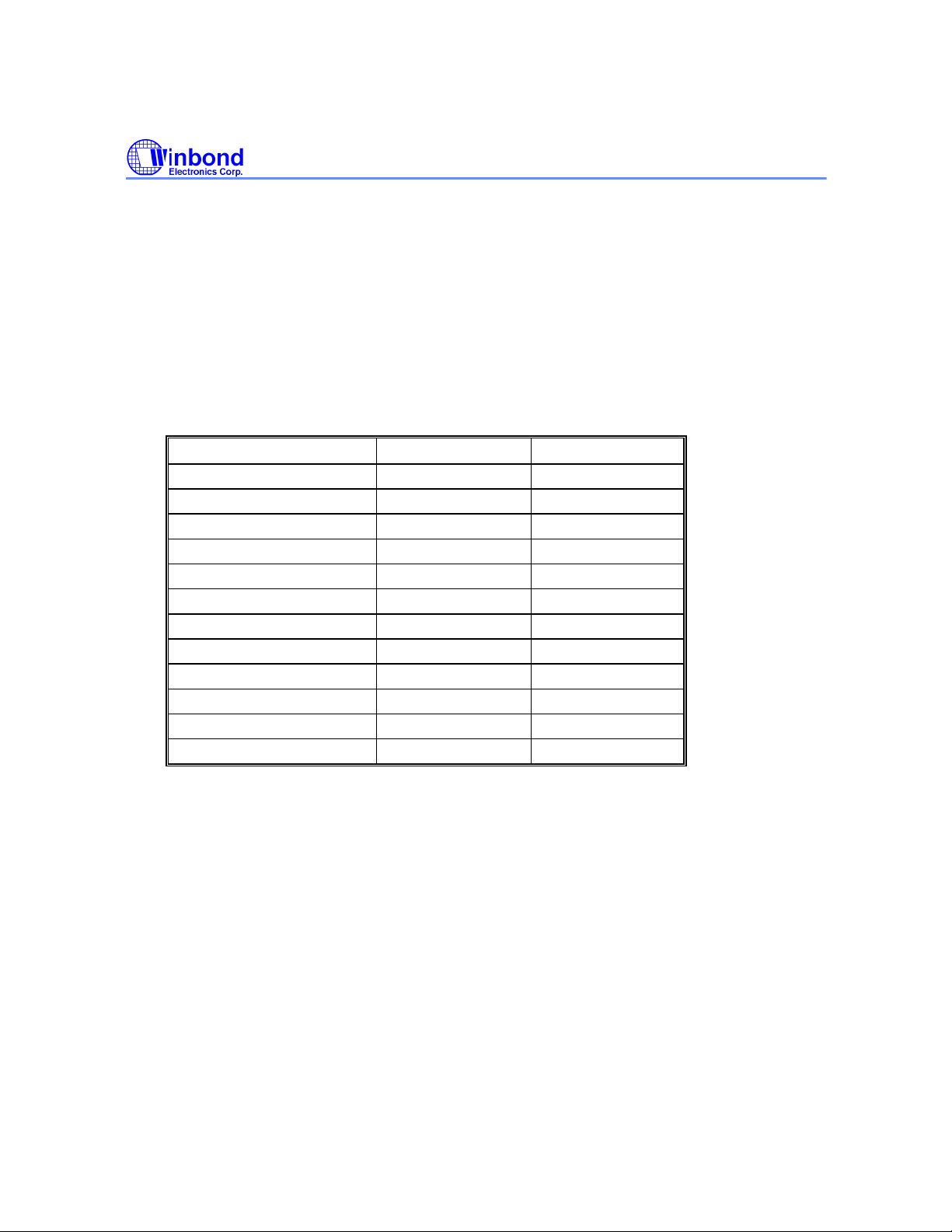
Preliminary W77C32
clearing a bit in the IE SFR. IE also has a global enable/disable bit EA, which can be cleared to
disable all the interrupts, except PFI, at once.
Priority Level Structure
There are two priority levels for the interrupts, high and low. The interrupt source can be individually
set to either high or low levels. Naturally, a higher priority interrupt cannot be interrupted by a lower
priority interrupt. However there exists a pre-defined hierarchy amongst the interrupts themselves.
This hierarchy comes into play when the interrupt controller has to resolve simultaneous requests
having the same priority level. This hierarchy is defined as shown below; the interrupts are numbered
starting from the highest priority to the lowest.
Table 7. Priority structure of interrupts
SOURCE FLAG PRIORITY LEVEL
External Interrupt 0 IE0 1 (highest)
Timer 0 Overflow TF0 2
External Interrupt 1 IE1 3
Timer 1 Overflow TF1 4
Serial Port RI + TI 5
Timer 2 Overflow TF2 + EXF2 6
Serial Port 1 RI_1 + TI_1 7
External Interrupt 2 IE2 8
External Interrupt 3 IE3 9
External Interrupt 4 IE4 10
External Interrupt 5 IE5 11
Watchdog Timer WDIF 12 (lowest)
The interrupt flags are sampled every machine cycle. In the same machine cycle, the sampled
interrupts are polled and their priority is resolved. If certain conditions are met then the hardware will
execute an internally generated LCALL instruction which will vector the process to the appropriate
interrupt vector address. The conditions for generating the LCALL are
1. An interrupt of equal or higher priority is not currently being serviced.
2. The current polling cycle is the last machine cycle of the instruction currently being executed.
3. The current instruction does not involve a write to IP, IE, EIP or EIE registers and is not a RETI.
If any of these conditions are not met, then the LCALL will not be generated. The polling cycle is
repeated every machine cycle, with the interrupts sampled in the same machine cycle. If an interrupt
flag is active in one cycle but not responded to, and is not active when the above conditions are met,
the denied interrupt will not be serviced. This means that active interrupts are not remembered; every
polling cycle is new.
Publication Release Date: March 1999
- 45 - Revision A1
Page 46
Preliminary W77C32
The processor responds to a valid interrupt by executing an LCALL instruction to the appropriate
service routine. This may or may not clear the flag which caused the interrupt. In case of Timer
interrupts, the TF0 or TF1 flags are cleared by hardware whenever the processor vectors to the
appropriate timer service routine. In case of external interrupt, INT0 and INT1, the flags are cleared
only if they are edge triggered. In case of Serial interrupts, the flags are not cleared by hardware. In
the case of Timer 2 interrupt, the flags are not cleared by hardware. The Power-Fail interrupt PFI flag
and Watchdog timer interrupt flag WDIF have to be cleared by software. The hardware LCALL
behaves exactly like the software LCALL instruction. This instruction saves the Program Counter
contents onto the Stack, but does not save the Program Status Word PSW. The PC is reloaded with
the vector address of that interrupt which caused the LCALL. These vector address for the different
sources are as follows.
Table 8. Vector locations for interrupt sources
SOURCE VECTOR ADDRESS SOURCE VECTOR ADDRESS
Timer 0 Overflow 000Bh External Interrupt 0 0003h
Timer 1 Overflow 001Bh External Interrupt 1 0013h
Timer 2 Interrupt 002Bh Serial Port 0023h
External Interrupt 2 0043h Serial Port 1 003Bh
External Interrupt 4 0053h External Interrupt 3 004Bh
Watchdog Timer 0063h External Interrupt 5 005Bh
The vector table is not evenly spaced; this is to accommodate future expansions to the device family.
Execution continues from the vectored address till an RETI instruction is executed. On execution of
the RETI instruction the processor pops the Stack and loads the PC with the contents at the top of the
stack. The user must take care that the status of the stack is restored to what is was after the
hardware LCALL, if the execution is to return to the interrupted program. The processor does not
notice anything if the stack contents are modified and will proceed with execution from the address
put back into PC. Note that a RET instruction would perform exactly the same process as a RETI
instruction, but it would not inform the Interrupt Controller that the interrupt service routine is
completed, and would leave the controller still thinking that the service routine is underway.
Interrupt Response Time
The response time for each interrupt source depends on several factors, such as the nature of the
interrupt and the instruction underway. In the case of external interrupts INT0 to INT5 , they are
sampled at C3 of every machine cycle and then their corresponding interrupt flags IEx will be set or
reset. The Timer 0 and 1 overflow flags are set at C3 of the machine cycle in which overflow has
occurred. These flag values are polled only in the next machine cycle. If a request is active and all
three conditions are met, then the hardware generated LCALL is executed. This LCALL itself takes
four machine cycles to be completed. Thus there is a minimum time of five machine cycles between
the interrupt flag being set and the interrupt service routine being executed.
A longer response time should be anticipated if any of the three conditions are not met. If a higher or
equal priority is being serviced, then the interrupt latency time obviously depends on the nature of the
service routine currently being executed. If the polling cycle is not the last machine cycle of the
instruction being executed, then an additional delay is introduced. The maximum response time (if no
other interrupt is in service) occurs if the W77C32 is performing a write to IE, IP, EIE or EIP and then
- 46 -
Page 47

Preliminary W77C32
executes a MUL or DIV instruction. From the time an interrupt source is activated, the longest
reaction time is 12 machine cycles. This includes 1 machine cycle to detect the interrupt, 2 machine
cycles to complete the IE, IP, EIE or EIP access, 5 machine cycles to complete the MUL or DIV
instruction and 4 machine cycles to complete the hardware LCALL to the interrupt vector location.
Thus in a single-interrupt system the interrupt response time will always be more than 5 machine
cycles and not more than 12 machine cycles. The maximum latency of 12 machine cycle is 48 clock
cycles. Note that in the standard 8051 the maximum latency is 8 machine cycles which equals 96
machine cycles. This is a 50% reduction in terms of clock periods.
PROGRAMMABLE TIMERS/COUNTERS
The W77C32 has three 16-bit programmable timer/counters and one programmable Watchdog timer.
The Watchdog timer is operationally quite different from the other two timers.
Timer/Counters 0 & 1
The W77C32 has two 16-bit Timer/Counters. Each of these Timer/Counters has two 8 bit registers
which form the 16 bit counting register. For Timer/Counter 0 they are TH0, the upper 8 bits register,
and TL0, the lower 8 bit register. Similarly Timer/Counter 1 has two 8 bit registers, TH1 and TL1. The
two can be configured to operate either as timers, counting machine cycles or as counters counting
external inputs.
When configured as a "Timer", the timer counts clock cycles. The timer clock can be programmed to
be thought of as 1/12 of the system clock or 1/4 of the system clock. In the "Counter" mode, the
register is incremented on the falling edge of the external input pin, T0 in case of Timer 0, and T1 for
Timer 1. The T0 and T1 inputs are sampled in every machine cycle at C4. If the sampled value is
high in one machine cycle and low in the next, then a valid high to low transition on the pin is
recognized and the count register is incremented. Since it takes two machine cycles to recognize a
negative transition on the pin, the maximum rate at which counting will take place is 1/24 of the
master clock frequency. In either the "Timer" or "Counter" mode, the count register will be updated at
C3. Therefore, in the "Timer" mode, the recognized negative transition on pin T0 and T1 can cause
the count register value to be updated only in the machine cycle following the one in which the
negative edge was detected.
The "Timer" or "Counter" function is selected by the "C/T" bit in the TMOD Special Function
Register. Each Timer/Counter has one selection bit for its own; bit 2 of TMOD selects the function for
Timer/Counter 0 and bit 6 of TMOD selects the function for Timer/Counter 1. In addition each
Timer/Counter can be set to operate in any one of four possible modes. The mode selection is done
by bits M0 and M1 in the TMOD SFR.
Time-base Selection
The W77C32 gives the user two modes of operation for the timer. The timers can be programmed to
operate like the standard 8051 family, counting at the rate of 1/12 of the clock speed. This will ensure
that timing loops on the W77C32 and the standard 8051 can be matched. This is the default mode of
operation of the W77C32 timers. The user also has the option to count in the turbo mode, where the
timers will increment at the rate of 1/4 clock speed. This will straight-away increase the counting
speed three times. This selection is done by the T0M and T1M bits in CKCON SFR. A reset sets
these bits to 0, and the timers then operate in the standard 8051 mode. The user should set these bits
to 1 if the timers are to operate in turbo mode.
Publication Release Date: March 1999
- 47 - Revision A1
Page 48
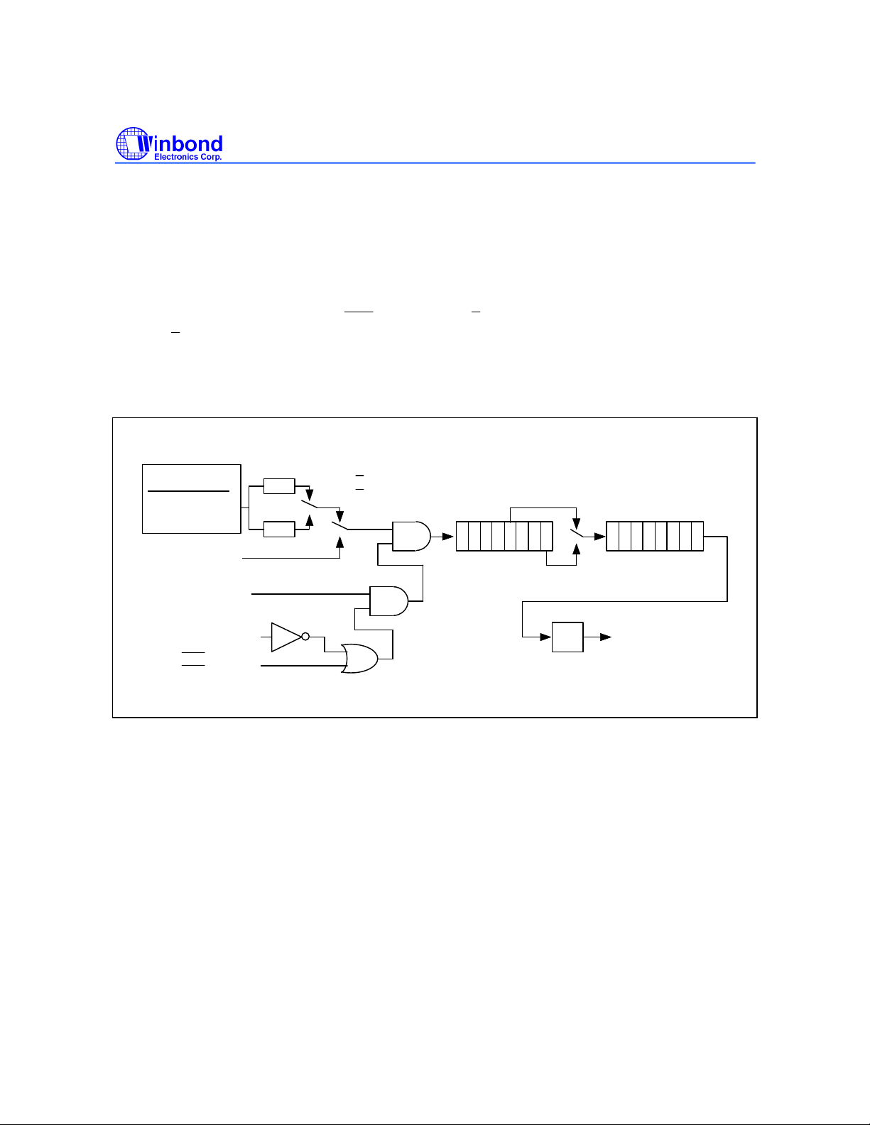
Preliminary W77C32
INTx
Mode 0
In Mode 0, the timer/counters act as a 8 bit counter with a 5 bit, divide by 32 pre-scale. In this mode
we have a 13 bit timer/counter. The 13 bit counter consists of 8 bits of THx and 5 lower bits of TLx.
The upper 3 bits of TLx are ignored.
The negative edge of the clock increments the count in the TLx register. When the fifth bit in TLx
moves from 1 to 0, then the count in the THx register is incremented. When the count in THx moves
from FFh to 00h, then the overflow flag TFx in TCON SFR is set. The counted input is enabled only if
TRx is set and either GATE = 0 or
and if C/T is set to 1, then it will count 1 to 0 transitions on T0 (P3.4) for timer 0 and T1 (P3.5) for
timer 1. When the 13 bit count reaches 1FFFh the next count will cause it to roll-over to 0000h. The
timer overflow flag TFx of the relevant timer is set and if enabled an interrupts will occur. Note that
when used as a timer, the time-base may be either clock cycles/12 or clock cycles/4 as selected by
the bits TxM of the CKCON SFR.
= 1. When C/T is set to 0, then it will count clock cycles,
Clock Source
Mode input
div. by 4 osc/1
div. by 64 osc/16
div. by 1024 osc/256
T0 = P3.4
(T1 = P3.5)
TR0 = TCON.4
(TR1 = TCON.6)
GATE = TMOD.3
(GATE = TMOD.7)
INT0 = P3.2
(INT1 = P3.3)
T0M = CKCON.3
(T1M = CKCON.4)
1/4
1
1/12
0
Figure 11: Timer/Counter Mode 0 & Mode 1
C/T = TMOD.2
(C/T = TMOD.6)
0
1
Timer 1 functions are shown in brackets
M1,M0 = TMOD.1,TMOD.0
(M1,M0 = TMOD.5,TMOD.4)
00
70
4 70
TL0
(TL1)
01
TFx
TF0
(TF1)
TH0
(TH1)
Interrupt
Mode 1
Mode 1 is similar to Mode 0 except that the counting register forms a 16 bit counter, rather than a 13
bit counter. This means that all the bits of THx and TLx are used. Roll-over occurs when the timer
moves from a count of FFFFh to 0000h. The timer overflow flag TFx of the relevant timer is set and if
enabled an interrupt will occur. The selection of the time-base in the timer mode is similar to that in
Mode 0. The gate function operates similarly to that in Mode 0.
Mode 2
In Mode 2, the timer/counter is in the Auto Reload Mode. In this mode, TLx acts as a 8 bit count
register, while THx holds the reload value. When the TLx register overflows from FFh to 00h, the TFx
bit in TCON is set and TLx is reloaded with the contents of THx, and the counting process continues
from here. The reload operation leaves the contents of the THx register unchanged. Counting is
- 48 -
Page 49
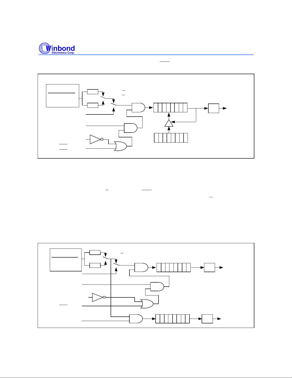
Preliminary W77C32
INTx
enabled by the TRx bit and proper setting of GATE and
pins. As in the other two modes 0 and
1, mode 2 allows counting of either clock cycles (clock/12 or clock/4) or pulses on pin Tn.
T0M = CKCON.3
Clock Source
Mode input
div. by 4 osc/1
div. by 64 osc/16
div. by 1024 osc/256
T0 = P3.4
(T1 = P3.5)
TR0 = TCON.4
(TR1 = TCON.6)
GATE = TMOD.3
(GATE = TMOD.7)
INT0 = P3.2
(INT1 = P3.3)
(T1M = CKCON.4)
1/4
1/12
1
0
Timer 1 functions are shown in brackets
C/T = TMOD.2
(C/T = TMOD.6)
0
1
Figure 12: Timer/Counter Mode 2
(TL1)
TH0
(TH1)
TL0
70
TFx
TF0
(TF1)
Interrupt
70
Mode 3
Mode 3 has different operating methods for the two timer/counters. For timer/counter 1, mode 3
simply freezes the counter. Timer/Counter 0, however, configures TL0 and TH0 as two separate 8 bit
count registers in this mode. The logic for this mode is shown in the figure. TL0 uses the
Timer/Counter 0 control bits C/T, GATE, TR0, INT0 and TF0. The TL0 can be used to count clock
cycles (clock/12 or clock/4) or 1-to-0 transitions on pin T0 as determined by C/T (TMOD.2). TH0 is
forced as a clock cycle counter (clock/12 or clock/4) and takes over the use of TR1 and TF1 from
Timer/Counter 1. Mode 3 is used in cases where an extra 8 bit timer is needed. With Timer 0 in Mode
3, Timer 1 can still be used in Modes 0, 1 and 2., but its flexibility is somewhat limited. While its basic
functionality is maintained, it no longer has control over its overflow flag TF1 and the enable bit TR1.
Timer 1 can still be used as a timer/counter and retains the use of GATE and INT1 pin. In this
condition it can be turned on and off by switching it out of and into its own Mode 3. It can also be used
as a baud rate generator for the serial port.
Clock Source
Mode input
div. by 4 osc/1
div. by 64 osc/16
div. by 1024 osc/256
T0 = P3.4
TR0 = TCON.4
GATE = TMOD.3
INT0 = P3.2
TR1 = TCON.6
T0M = CKCON.3
1/4
1/12
1
C/T = TMOD.2
0
0
1
Figure 13. Timer/Counter 0 Mode 3
- 49 - Revision A1
TL0
Interrupt
Interrupt
TH0
70
TF0
TF170
Publication Release Date: March 1999
Page 50
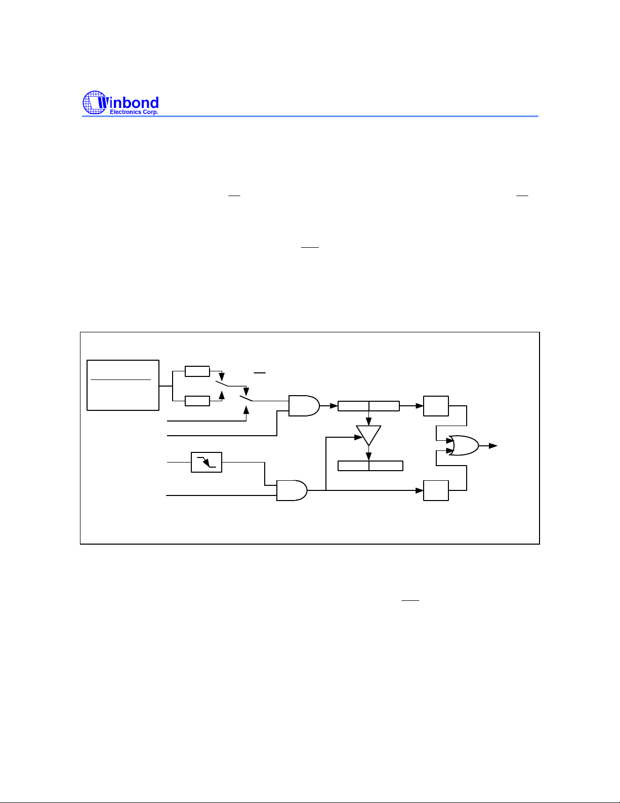
Preliminary W77C32
RL2
RL2
Timer/Counter 2
Timer/Counter 2 is a 16 bit up/down counter which is configured by the T2MOD register and
controlled by the T2CON register. Timer/Counter 2 is equipped with a capture/reload capability. As
with the Timer 0 and Timer 1 counters, there exists considerable flexibility in selecting and controlling
the clock, and in defining the operating mode. The clock source for Timer/Counter 2 may be selected
for either the external T2 pin (C/T2 = 1) or the crystal oscillator, which is divided by 12 or 4 (C/T2 =
0). The clock is then enabled when TR2 is a 1, and disabled when TR2 is a 0.
Capture Mode
The capture mode is enabled by setting the CP/
bit in the T2CON register to a 1. In the capture
mode, Timer/Counter 2 serves as a 16 bit up counter. When the counter rolls over from FFFFh to
0000h, the TF2 bit is set, which will generate an interrupt request. If the EXEN2 bit is set, then a
negative transition of T2EX pin will cause the value in the TL2 and TH2 register to be captured by the
RCAP2L and RCAP2H registers. This action also causes the EXF2 bit in T2CON to be set, which will
also generate an interrupt. Setting the T2CR bit (T2MOD.3), the W77C32 allows hardware to reset
timer 2 automatically after the value of TL2 and TH2 have been captured.
Clock Source
Mode input
div. by 4 osc/1
div. by 64 osc/16
div. by 1024 osc/256
T2 = P1.0
TR2 = T2CON.2
T2EX = P1.1
EXEN2 = T2CON.3
T2M = CKCON.5
1/4
1/12
1
C/T2 = T2CON.1
0
0
L
TH2TL2
RCAP2H
HH
1
RCAP2L
T2CON.7
TF2
Timer 2
Interrupt
EXF2
T2CON.6
Figure 14. 16-Bit Capture Mode
Auto-reload Mode, Counting Up
The auto-reload mode as an up counter is enabled by clearing the CP/
bit in the T2CON register
and clearing the DCEN bit in T2MOD register. In this mode, Timer/Counter 2 is a 16 bit up counter.
When the counter rolls over from FFFFh, a reload is generated that causes the contents of the
RCAP2L and RCAP2H registers to be reloaded into the TL2 and TH2 registers. The reload action also
sets the TF2 bit. If the EXEN2 bit is set, then a negative transition of T2EX pin will also cause a
reload. This action also sets the EXF2 bit in T2CON.
- 50 -
Page 51
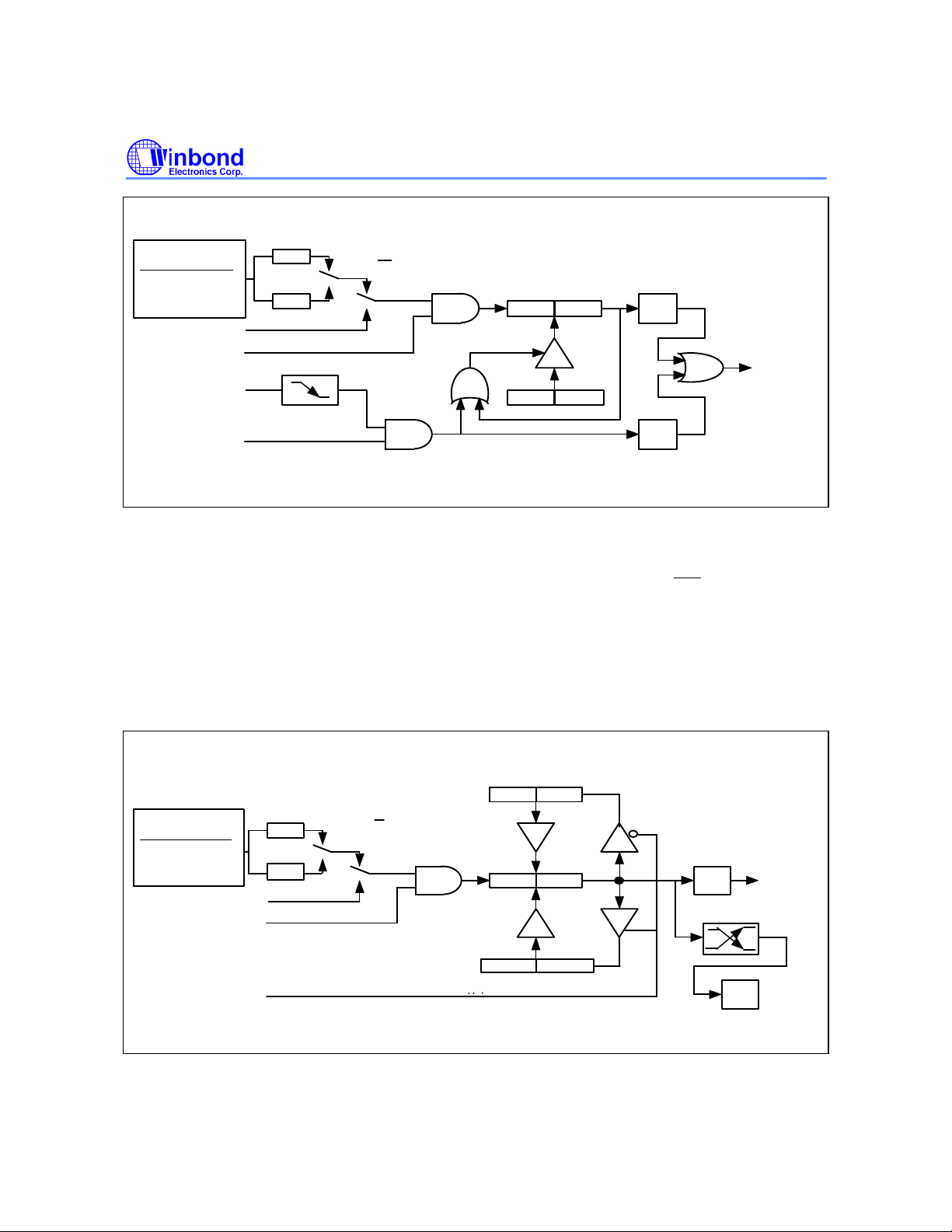
Preliminary W77C32
RL2
Clock Source
Mode input
div. by 4 osc/1
div. by 64 osc/16
div. by 1024 osc/256
T2 = P1.0
TR2 = T2CON.2
T2EX = P1.1
T2M = CKCON.5
1/4
1/12
1
C/T2 = T2CON.1
0
0
1
T2CON.7
TH2TL2
TF2
Timer 2
Interrupt
RCAP2HRCAP2L
L
EXEN2 = T2CON.3
Figure 15. 16-Bit Auto-reload Mode, Counting Up
EXF2
T2CON.6
Auto-reload Mode, Counting Up/Down
Timer/Counter 2 will be in auto-reload mode as an up/down counter if CP/
bit in T2CON is
cleared and the DCEN bit in T2MOD is set. In this mode, Timer/Counter 2 is an up/down counter
whose direction is controlled by the T2EX pin. A 1 on this pin cause the counter to count up. An
overflow while counting up will cause the counter to be reloaded with the contents of the capture
registers. The next down count following the case where the contents of Timer/Counter equal the
capture registers will load an FFFFh into Timer/Counter 2. In either event a reload will set the TF2 bit.
A reload will also toggle the EXF2 bit. However, the EXF2 bit can not generate an interrupt while in
this mode.
Clock Source
Mode input
div. by 4 osc/1
div. by 64 osc/16
div. by 1024 osc/256
T2 = P1.0
TR2 = T2CON.2
T2EX = P1.1
T2M = CKCON.5
1/4
1/12
Down Counting Reload Value
0FFh0FFh
C/T = T2CON.1
1
0
0
1
RCAP2HRCAP2L
Up Counting Reload
DCEN = 1
Figure 16. 16-Bit Auto-reload Up/Down Counter
- 51 - Revision A1
.7
T2CON
TH2TL2
TF2
EXF2
T2CON.6
Publication Release Date: March 1999
Timer 2
Interrupt
Page 52
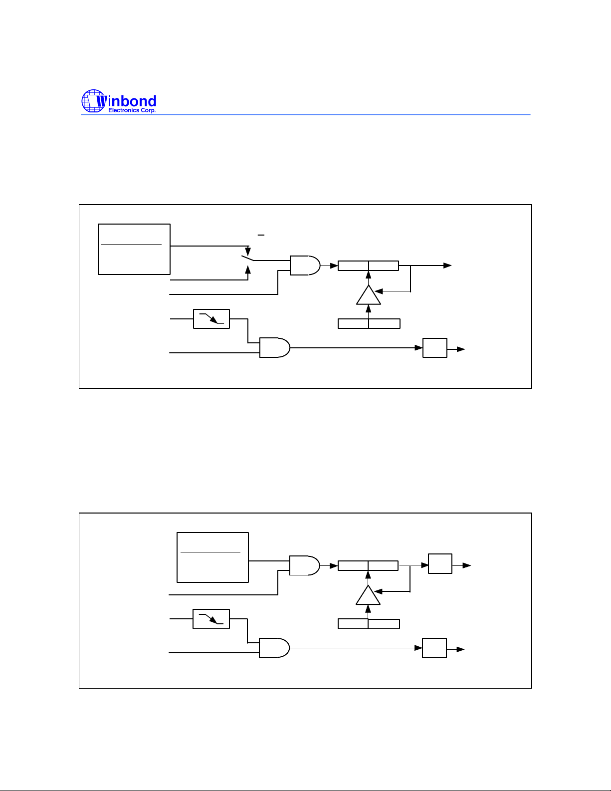
Preliminary W77C32
BAUD RATE GENERATOR MODE
The baud rate generator mode is enabled by setting either the RCLK or TCLK bits in T2CON register.
While in the baud rate generator mode, Timer/Counter 2 is a 16 bit counter with auto reload when the
count rolls over from FFFFh. However, rolling over does not set the TF2 bit. If EXEN2 bit is set, then
a negative transition of the T2EX pin will set EXF2 bit in the T2CON register and cause an interrupt
request.
Clock Source
Mode input
div. by 4 osc/2
div. by 64 osc/32
div. by 1024 osc/512
T2 = P1.0
TR2 = T2CON.2
T2EX = P1.1
EXEN2 = T2CON.3
C/T = T2CON.1
0
1
Figure 17. Baud Rate Generator Mode
TH2TL2
RCAP2HRCAP2L
EXF2
T2CON.6
Timer 2
overflow
Timer 2
Interrupt
Programmable Clock-out
Timer 2 is equipped with a new clock-out feature which outputs a 50% duty cycle clock on P1.0. It can
be invoked as a programmable clock generator. To configure Timer 2 with clock-out mode, software
must initiate it by setting bit T2OE = 1, C/T2 = 0 and CP/RL = 0. Setting bit TR2 will start the timer.
This mode is similar to the baud rate generator mode, it will not generate an interrupt while Timer 2
overflow. So it is possible to use Timer 2 as a baud rate generator and a clock generator at the same
time. The clock-out frequency is determined by the following equation:
The Clock-out Frequency = Oscillator Frequency / [4 X (RCAP2H,RCAP2L) ]
TR2 = T2CON.2
T2EX = P1.1
EXEN2 = T2CON.3
Clock Source
Mode input
div. by 4 osc/2
div. by 64 osc/32
div. by 1024 osc/512
Figure 18. Programmable Clock-Out Mode
- 52 -
TH2TL2
RCAP2HRCAP2L
1/2
EXF2
T2CON.6
T2=P1.0
Timer 2
Interrupt
Page 53
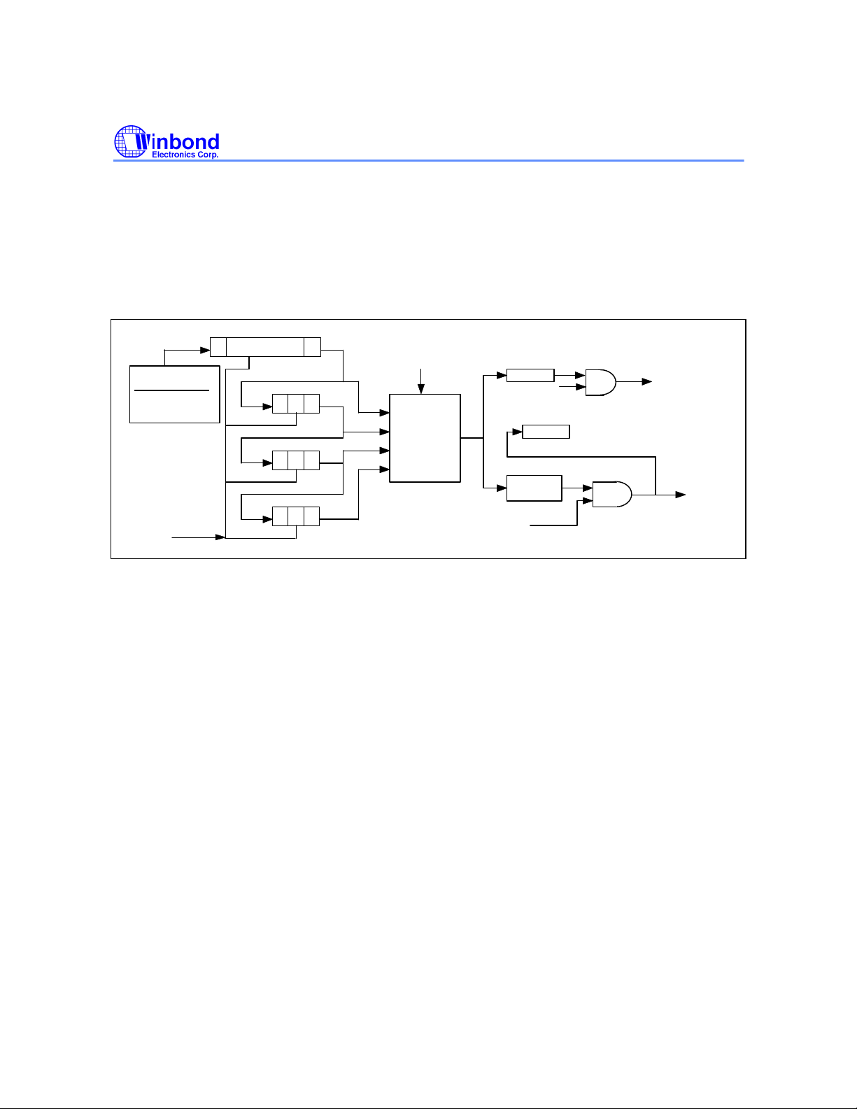
Preliminary W77C32
Watchdog Timer
The Watchdog timer is a free-running timer which can be programmed by the user to serve as a
system monitor, a time-base generator or an event timer. It is basically a set of dividers that divide
the system clock. The divider output is selectable and determines the time-out interval. When the
time-out occurs a flag is set, which can cause an interrupt if enabled, and a system reset can also be
caused if it is enabled. The interrupt will occur if the individual interrupt enable and the global enable
are set. The interrupt and reset functions are independent of each other and may be used separately
or together depending on the users software.
17 19
20 22
23 25
16
WD1,WD0
00
01
Time-out
10
11
Enable Watchdog timer reset
EWT(WDCON.1)
Figure 19. Watchdog Timer
WDIF
EWDI(EIE.4)
WTRF
512 clock
delay
Interrupt
Reset
Clock Source
Mode input
div. by 4 osc/1
div. by 64 osc/16
div. by 1024 osc/256
Reset Watchdog
RWT (WDCON.0)
0
The Watchdog timer should first be restarted by using RWT. This ensures that the timer starts from a
known state. The RWT bit is used to restart the watchdog timer. This bit is self clearing, i.e. after
writing a 1 to this bit the software will automatically clear it. The watchdog timer will now count clock
cycles. The time-out interval is selected by the two bits WD1 and WD0 (CKCON.7 and CKCON.6).
When the selected time-out occurs, the Watchdog interrupt flag WDIF (WDCON.3) is set. After the
time-out has occurred, the watchdog timer waits for an additional 512 clock cycles. If the Watchdog
Reset EWT (WDCON.1) is enabled, then 512 clocks after the time-out, if there is no RWT, a system
reset due to Watchdog timer will occur. This will last for two machine cycles, and the Watchdog timer
reset flag WTRF (WDCON.2) will be set. This indicates to the software that the watchdog was the
cause of the reset.
When used as a simple timer, the reset and interrupt functions are disabled. The timer will set the
WDIF flag each time the timer completes the selected time interval. The WDIF flag is polled to detect
a time-out and the RWT allows software to restart the timer. The Watchdog timer can also be used as
a very long timer. The interrupt feature is enabled in this case. Every time the time-out occurs an
interrupt will occur if the global interrupt enable EA is set.
The main use of the Watchdog timer is as a system monitor. This is important in real-time control
applications. In case of some power glitches or electro-magnetic interference, the processor may
begin to execute errant code. If this is left unchecked the entire system may crash. Using the
watchdog timer interrupt during software development will allow the user to select ideal watchdog
reset locations. The code is first written without the watchdog interrupt or reset. Then the watchdog
interrupt is enabled to identify code locations where interrupt occurs. The user can now insert
instructions to reset the watchdog timer which will allow the code to run without any watchdog timer
interrupts. Now the watchdog timer reset is enabled and the watchdog interrupt may be disabled,. If
Publication Release Date: March 1999
- 53 - Revision A1
Page 54
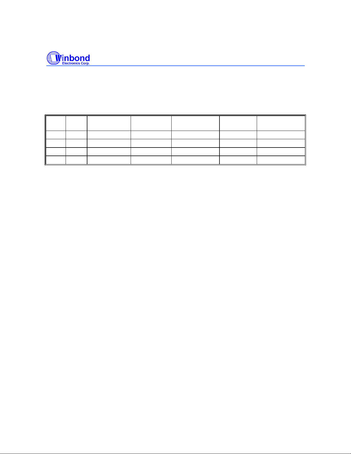
Preliminary W77C32
any errant code is executed now, then the reset watchdog timer instructions will not be executed at
the required instants and watchdog reset will occur.
The watchdog time-out selection will result in different time-out values depending on the clock speed.
The reset, when enabled, will occur 512 clocks after the time-out has occurred.
Table 9. Time-out values for the Watchdog timer
WD1 WD0 WATCHDOGI
NTERVAL
0 0 2
0 1 2
1 0 2
1 1 2
17
20
23
26
NUMBER OF
CLOCKS
131072 71.11 mS 13.11 mS 5.24 mS
1048576 568.89 mS 104.86 mS 41.94 mS
8388608 4551.11 mS 838.86 mS 335.54 mS
67108864 36408.88 mS 6710.89 mS 2684.35 mS
TIME
@1.8432 MHz
TIME
@10 MHz
TIME
@25 MHz
The Watchdog timer will de disabled by a power-on/fail reset. The Watchdog timer reset does not
disable the watchdog timer, but will restart it. In general, software should restart the timer to put it into
a known state.
The control bits that support the Watchdog timer are discussed below.
WATCHDOG CONTROL
WDIF: WDCON.3 - Watchdog Timer Interrupt flag. This bit is set whenever the time-out occurs in
the watchdog timer. If the Watchdog interrupt is enabled (EIE.4), then an interrupt will occur
(if the global interrupt enable is set and other interrupt requirements are met). Software or any
reset can clear this bit.
WTRF: WDCON.2 - Watchdog Timer Reset flag. This bit is set whenever a watchdog reset occurs.
This bit is useful for determined the cause of a reset. Software must read it, and clear it
manually. A Power-fail reset will clear this bit. If EWT = 0, then this bit will not be affected by
the watchdog timer.
EWT: WDCON.1 - Enable Watchdog timer Reset. This bit when set to 1 will enable the Watchdog
timer reset function. Setting this bit to 0 will disable the Watchdog timer reset function, but
will leave the timer running
RWT: WDCON.0 - Reset Watchdog Timer. This bit is used to clear the Watchdog timer and to
restart it. This bit is self-clearing, so after the software writes 1 to it the hardware will
automatically clear it. If the Watchdog timer reset is enabled, then the RWT has to be set by
the user within 512 clocks of the time-out. If this is not done then a Watchdog timer reset will
occur.
CLOCK CONTROL
WD1,WD0: CKCON.7, CKCON.6 - Watchdog Timer Mode select bits. These two bits select the time-
out interval for the watchdog timer. The reset time is 512 clock longer than the interrupt
time-out value.
The default Watchdog time-out is 217 clocks, which is the shortest time-out period. The EWT, WDIF
and RWT bits are protected by the Timed Access procedure. This prevents software from accidentally
enabling or disabling the watchdog timer. More importantly, it makes it highly improbable that errant
code can enable or disable the watchdog timer.
- 54 -
Page 55
Preliminary W77C32
Serial Port
Serial port in the W77C32 is a full duplex port. The W77C32 provides the user with additional
features such as the Frame Error Detection and the Automatic Address Recognition. The serial ports
are capable of synchronous as well as asynchronous communication. In Synchronous mode the
W77C32 generates the clock and operates in a half duplex mode. In the asynchronous mode, full
duplex operation is available. This means that it can simultaneously transmit and receive data. The
transmit register and the receive buffer are both addressed as SBUF Special Function Register.
However any write to SBUF will be to the transmit register, while a read from SBUF will be from the
receive buffer register. The serial port can operate in four different modes as described below.
Mode 0
This mode provides synchronous communication with external devices. In this mode serial data is
transmitted and received on the RXD line. TXD is used to transmit the shift clock. The TxD clock is
provided by the W77C32 whether the device is transmitting or receiving. This mode is therefore a half
duplex mode of serial communication. In this mode, 8 bits are transmitted or received per frame. The
LSB is transmitted/received first. The baud rate is fixed at 1/12 or 1/4 of the oscillator frequency. This
baud rate is determined by the SM2 bit (SCON.5). When this bit is set to 0, then the serial port runs at
1/12 of the clock. When set to 1, the serial port runs at 1/4 of the clock. This additional facility of
programmable baud rate in mode 0 is the only difference between the standard 8051 and the
W77C32.
The functional block diagram is shown below. Data enters and leaves the Serial port on the RxD line.
The TxD line is used to output the shift clock. The shift clock is used to shift data into and out of the
W77C32 and the device at the other end of the line. Any instruction that causes a write to SBUF will
start the transmission. The shift clock will be activated and data will be shifted out on the RxD pin till
all 8 bits are transmitted. If SM2 = 1, then the data on RxD will appear 1 clock period before the
falling edge of shift clock on TxD. The clock on TxD then remains low for 2 clock periods, and then
goes high again. If SM2 = 0, the data on RxD will appear 3 clock periods before the falling edge of
shift clock on TxD. The clock on TxD then remains low for 6 clock periods, and then goes high again.
This ensures that at the receiving end the data on RxD line can either be clocked on the rising edge
of the shift clock on TxD or latched when the TxD clock is low.
Clock Source
Mode input
div. by 4 osc/1
div. by 64 osc/16
div. by 1024 osc/256
÷4÷12
SM2
10
RI
REN
P3.0 Alternate
Iutput function
RXD
Write to
SBUF
TX START
TX CLOCK
CONTROLLER
RX
CLOCK
RX
START
Internal
Data Bus
CLOCK
TX SHIFT
TI
SERIAL
Figure 20. Serial Port Mode 0
RI
SHIFT
CLOCK
LOAD SBUF
RX SHIFT
Transmit Shift Register
CLOCK
PAROUT
SIN
Receive Shift Register
PARIN
LOAD
SOUT
RXD
P3.0 Alternate
Output Function
Serial Port Interrupt
TXD
P3.1 Alternate
Output function
SBUF
Read SBUF
SBUF
Data Bus
Internal
Publication Release Date: March 1999
- 55 - Revision A1
Page 56

Preliminary W77C32
The TI flag is set high in C1 following the end of transmission of the last bit. The serial port will
receive data when REN is 1 and RI is zero. The shift clock (TxD) will be activated and the serial port
will latch data on the rising edge of shift clock. The external device should therefore present data on
the falling edge on the shift clock. This process continues till all the 8 bits have been received. The RI
flag is set in C1 following the last rising edge of the shift clock on TxD. This will stop reception, till the
RI is cleared by software.
Mode 1
In Mode 1, the full duplex asynchronous mode is used. Serial communication frames are made up of
10 bits transmitted on TXD and received on RXD. The 10 bits consist of a start bit (0), 8 data bits
(LSB first), and a stop bit (1). On receive, the stop bit goes into RB8 in the SFR SCON. The baud rate
in this mode is variable. The serial baud can be programmed to be 1/16 or 1/32 of the Timer 1
overflow. Since the Timer 1 can be set to different reload values, a wide variation in baud rates is
possible.
Transmission begins with a write to SBUF. The serial data is brought out on to TxD pin at C1
following the first roll-over of divide by 16 counter. The next bit is placed on TxD pin at C1 following
the next rollover of the divide by 16 counter. Thus the transmission is synchronized to the divide by
16 counter and not directly to the write to SBUF signal. After all 8 bits of data are transmitted, the stop
bit is transmitted. The TI flag is set in the C1 state after the stop bit has been put out on TxD pin. This
will be at the 10th rollover of the divide by 16 counter after a write to SBUF.
Reception is enabled only if REN is high. The serial port actually starts the receiving of serial data,
with the detection of a falling edge on the RxD pin. The 1-to-0 detector continuously monitors the RxD
line, sampling it at the rate of 16 times the selected baud rate. When a falling edge is detected, the
divide by 16 counter is immediately reset. This helps to align the bit boundaries with the rollovers of
the divide by 16 counter.
The 16 states of the counter effectively divide the bit time into 16 slices. The bit detection is done on
a best of three basis. The bit detector samples the RxD pin, at the 8th, 9th and 10th counter states.
By using a majority 2 of 3 voting system, the bit value is selected. This is done to improve the noise
rejection feature of the serial port. If the first bit detected after the falling edge of RxD pin is not 0,
then this indicates an invalid start bit, and the reception is immediately aborted. The serial port again
looks for a falling edge in the RxD line. If a valid start bit is detected, then the rest of the bits are also
detected and shifted into the SBUF.
After shifting in 8 data bits, there is one more shift to do, after which the SBUF and RB8 are loaded
and RI is set. However certain conditions must be met before the loading and setting of RI can be
done.
1. RI must be 0 and
2. Either SM2 = 0, or the received stop bit = 1.
If these conditions are met, then the stop bit goes to RB8, the 8 data bits go into SBUF and RI is set.
Otherwise the received frame may be lost. After the middle of the stop bit, the receiver goes back to
looking for a 1-to-0 transition on the RxD pin.
- 56 -
Page 57
Preliminary W77C32
Timer 1
Overflow
SMOD=
(SMOD_1)
TCLK
RCLK
÷2
0 1
RXD
Timer 2 Overflow
(for Serial Port 0 only)
0 1
10
÷
16
SAMPLE
1-TO-0
DETECTOR
Internal
Write to
SBUF
TX START
÷
16
TX CLOCK
CONTROLLER
RX CLOCK
START
DETECTOR
Data Bus
TX SHIFT
TI
SERIAL
RX
BIT
Figure 21: Serial Port Mode
RI
LOAD
SBUF
RX SHIFT
Transmit Shift Register
STOP
PARIN
SOUT
START
LOAD
CLOCK
CLOCK
PAROUT
SIN
Receive Shift Register
D8
SBUF
RB8
TXD
Serial Port
Interrupt
Read
SBUF
Internal
Data
Bus
Mode 2
This mode uses a total of 11 bits in asynchronous full-duplex communication. The functional
description is shown in the figure below. The frame consists of one start bit (0), 8 data bits (LSB first),
a programmable 9th bit (TB8) and a stop bit (0). The 9th bit received is put into RB8. The baud rate is
programmable to 1/32 or 1/64 of the oscillator frequency, which is determined by the SMOD bit in
PCON SFR. Transmission begins with a write to SBUF. The serial data is brought out on to TxD pin
at C1 following the first roll-over of the divide by 16 counter. The next bit is placed on TxD pin at C1
following the next rollover of the divide by 16 counter. Thus the transmission is synchronized to the
divide by 16 counter, and not directly to the write to SBUF signal. After all 9 bits of data are
transmitted, the stop bit is transmitted. The TI flag is set in the C1 state after the stop bit has been put
out on TxD pin. This will be at the 11th rollover of the divide by 16 counter after a write to SBUF.
Reception is enabled only if REN is high. The serial port actually starts the receiving of serial data,
with the detection of a falling edge on the RxD pin. The 1-to-0 detector continuously monitors the RxD
line, sampling it at the rate of 16 times the selected baud rate. When a falling edge is detected, the
divide by 16 counter is immediately reset. This helps to align the bit boundaries with the rollovers of
the divide by 16 counter. The 16 states of the counter effectively divide the bit time into 16 slices. The
bit detection is done on a best of three basis. The bit detector samples the RxD pin, at the 8th, 9th
and 10th counter states. By using a majority 2 of 3 voting system, the bit value is selected. This is
done to improve the noise rejection feature of the serial port. If the first bit detected after the falling
edge of RxD pin, is not 0, then this indicates an invalid start bit, and the reception is immediately
aborted. The serial port again looks for a falling edge in the RxD line. If a valid start bit is detected,
then the rest of the bits are also detected and shifted into the SBUF. After shifting in 9 data bits, there
Publication Release Date: March 1999
- 57 - Revision A1
Page 58
Preliminary W77C32
is one more shift to do, after which the SBUF and RB8 are loaded and RI is set. However certain
conditions must be met before the loading and setting of RI can be done.
1. RI must be 0 and
2. Either SM2 = 0, or the received stop bit = 1.
If these conditions are met, then the stop bit goes to RB8, the 8 data bits go into SBUF and RI is set.
Otherwise the received frame may be lost. After the middle of the stop bit, the receiver goes back to
looking for a 1-to-0 transition on the RxD pin.
Clock Source
Mode input
div. by 4 osc/2
div. by 64 osc/32
div. by 1024 osc/512
÷
2
SMOD=
(SMOD_1)
0 1
SAMPLE
RXD
÷
16
÷
16
1-TO-0
DETECTOR
Write to
SBUF
TX START
TX CLOCK
RX CLOCK
RX START
Internal
Data Bus
SERIAL
CONTROLLER
BIT
DETECTOR
TB8
TX
SHIFT
TI
RI
LOAD
SBUF
RX SHIFT
D8
STOP
PARIN
SOUT
START
LOAD
CLOCK
Transmit Shift Register
CLOCK
PAROUT
SIN
Receive Shift Register
D8
T
SBUF
RB8
TXD
Serial Port
Interrupt
Read
SBUF
Internal
Data
Bus
Figure 22. Serial Port Mode 2
Mode 3
This mode is similar to Mode 2 in all respects, except that the baud rate is programmable. The user
must first initialize the Serial related SFR SCON before any communication can take place. This
involves selection of the Mode and baud rate. The Timer 1 should also be initialized if modes 1 and 3
are used. In all four modes, transmission is started by any instruction that uses SBUF as a destination
register. Reception is initiated in Mode 0 by the condition RI = 0 and REN = 1. This will generate a
clock on the TxD pin and shift in 8 bits on the RxD pin. Reception is initiated in the other modes by
the incoming start bit if REN = 1. The external device will start the communication by transmitting the
start bit.
- 58 -
Page 59
Table 10. Serial Ports Modes
Preliminary W77C32
SM1 SM0 MODE TYPE BAUD CLOCK FRAME
SIZE
START
BIT
STOP
BIT
9TH BIT
FUNCTION
0 0 0 Synch. 4 or 12 TCLKs 8 bits No No None
0 1 1 Asynch. Timer 1 or 2 10 bits 1 1 None
1 0 2 Asynch.
32 or 64 TCLKs
11 bits 1 1 0, 1
1 1 3 Asynch. Timer 1 or 2 11 bits 1 1 0, 1
Timer 1
Overflow
SMOD=
(SMOD_1)
TCLK
RCLK
÷2
0
Timer 2 Overflow
(for Serial Port 0 only)
1
0 1
10
÷
16
SAMPLE
1-TO-0
DETECTOR
÷16
Write to
SBUF
TX START
TX CLOCK
CONTROLLER
RX CLOCK
RX
START
SERIAL
Internal
Data Bus
TX SHIFT
LOAD
SBUF
RX SHIFT
TI
RI
TB8
STOP
D8
PARIN
SOUT
START
LOAD
CLOCK
Transmit Shift Register
TXD
Serial Port
Interrupt
Read
SBUF
RXD
BIT
DETECTOR
Figure 23: Serial Port Mode 3
CLOCK
PAROUT
SIN
Receive Shift Register
D8
SBUF
RB8
Internal
Data
Bus
Framing Error Detection
A Frame Error occurs when a valid stop bit is not detected. This could indicate incorrect serial data
communication. Typically the frame error is due to noise and contention on the serial communication
line. The W77C32 has the facility to detect such framing errors and set a flag which can be checked
by software.
The Frame Error FE(FE_1) bit is located in SCON.7(SCON1.7). This bit is normally used as SM0 in
the standard 8051 family. However, in the W77C32 it serves a dual function and is called SM0/FE
(SM0_1/FE_1). There are actually two separate flags, one for SM0 and the other for FE. The flag that
is actually accessed as SCON.7(SCON1.7) is determined by SMOD0 (PCON.6) bit. When SMOD0 is
Publication Release Date: March 1999
- 59 - Revision A1
Page 60

Preliminary W77C32
set to 1, then the FE flag is indicated in SM0/FE. When SMOD0 is set to 0, then the SM0 flag is
indicated in SM0/FE.
The FE bit is set to 1 by hardware but must be cleared by software. Note that SMOD0 must be 1 while
reading or writing to FE or FE_1. If FE is set, then any following frames received without any error will
not clear the FE flag. The clearing has to be done by software.
Multiprocessor Communications
Multiprocessor communications makes use of the 9th data bit in modes 2 and 3. In the W77C32, the
RI flag is set only if the received byte corresponds to the Given or Broadcast address. This hardware
feature eliminates the software overhead required in checking every received address, and greatly
simplifies the software programmer task.
In the multiprocessor communication mode, the address bytes are distinguished from the data bytes
by transmitting the address with the 9th bit set high. When the master processor wants to transmit a
block of data to one of the slaves, it first sends out the address of the targeted slave (or slaves). All
the slave processors should have their SM2 bit set high when waiting for an address byte. This
ensures that they will be interrupted only by the reception of a address byte. The Automatic address
recognition feature ensures that only the addressed slave will be interrupted. The address comparison
is done in hardware not software.
The addressed slave clears the SM2 bit, thereby clearing the way to receive data bytes. With SM2 =
0, the slave will be interrupted on the reception of every single complete frame of data. The
unaddressed slaves will be unaffected, as they will be still waiting for their address. In Mode 1, the 9th
bit is the stop bit, which is 1 in case of a valid frame. If SM2 is 1, then RI is set only if a valid frame is
received and the received byte matches the Given or Broadcast address.
The Master processor can selectively communicate with groups of slaves by using the Given
Address. All the slaves can be addressed together using the Broadcast Address. The addresses for
each slave are defined by the SADDR and SADEN SFRs. The slave address is an 8-bit value
specified in the SADDR SFR. The SADEN SFR is actually a mask for the byte value in SADDR. If a
bit position in SADEN is 0, then the corresponding bit position in SADDR is don't care. Only those bit
positions in SADDR whose corresponding bits in SADEN are 1 are used to obtain the Given Address.
This gives the user flexibility to address multiple slaves without changing the slave address in
SADDR.
The following example shows how the user can define the Given Address to address different slaves.
Slave 1:
SADDR1010 0100
SADEN1111 1010
Given 1010 0x0x
Slave 2:
SADDR1010 0111
SADEN1111 1001
Given 1010 0xx1
The Given address for slave 1 and 2 differ in the LSB. For slave 1, it is a don't care, while for slave 2
it is 1. Thus to communicate only with slave 1, the master must send an address with LSB = 0 (1010
0000). Similarly the bit 1 position is 0 for slave 1 and don't care for slave 2. Hence to communicate
only with slave 2 the master has to transmit an address with bit 1 = 1 (1010 0011). If the master
- 60 -
Page 61

Preliminary W77C32
wishes to communicate with both slaves simultaneously, then the address must have bit 0 = 1 and bit
1 = 0. The bit 3 position is don't care for both the slaves. This allows two different addresses to select
both slaves (1010 0001 and 1010 0101).
The master can communicate with all the slaves simultaneously with the Broadcast Address. This
address is formed from the logical ORing of the SADDR and SADEN SFRs. The zeros in the result
are defined as don't cares In most cases the Broadcast Address is FFh. In the previous case, the
Broadcast Address is (1111111X) for slave 1 and (11111111) for slave 2.
The SADDR and SADEN SFRs are located at address A9h and B9h respectively. On reset, these two
SFRs are initialized to 00h. This results in Given Address and Broadcast Address being set as XXXX
XXXX(i.e. all bits don't care). This effectively removes the multiprocessor communications feature,
since any selectivity is disabled.
Timed Access Protection
The W77C32 has several new features, like the Watchdog timer, on-chip ROM size adjustment, wait
state control signal and Power on/fail reset flag, which are crucial to proper operation of the system. If
left unprotected, errant code may write to the Watchdog control bits resulting in incorrect operation
and loss of control. In order to prevent this, the W77C32 has a protection scheme which controls the
write access to critical bits. This protection scheme is done using a timed access.
In this method, the bits which are to be protected have a timed write enable window. A write is
successful only if this window is active, otherwise the write will be discarded. This write enable
window is open for 3 machine cycles if certain conditions are met. After 3 machine cycles, this
window automatically closes. The window is opened by writing AAh and immediately 55h to the Timed
Access(TA) SFR. This SFR is located at address C7h. The suggested code for opening the timed
access window is
TA REG 0C7h ;define new register TA, located at 0C7h
MOV TA, #0AAh
MOV TA, #055h
When the software writes AAh to the TA SFR, a counter is started. This counter waits for 3 machine
cycles looking for a write of 55h to TA. If the second write (55h) occurs within 3 machine cycles of the
first write (AAh), then the timed access window is opened. It remains open for 3 machine cycles,
during which the user may write to the protected bits. Once the window closes the procedure must be
repeated to access the other protected bits.
Examples of Timed Assessing are shown below.
Example 1: Valid access
MOV TA, #0AAh 3 M/C Note: M/C = Machine Cycles
MOV TA, #055h 3 M/C
MOV WDCON, #00h 3 M/C
Example 2: Valid access
MOV TA, #0AAh 3 M/C
MOV TA, #055h 3 M/C
NOP 1 M/C
SETB EWT 2 M/C
Publication Release Date: March 1999
- 61 - Revision A1
Page 62
Preliminary W77C32
Example 3: Invalid access
MOV TA, #0AAh 3 M/C
MOV TA, #055h 3 M/C
NOP 1 M/C
NOP 1 M/C
CLR POR 2 M/C
Example 4: Invalid Access
MOV TA, #0AAh 3 M/C
NOP 1 M/C
MOV TA, #055h 3 M/C
SETB EWT 2 M/C
In the first two examples, the writing to the protected bits is done before the 3 machine cycle window
closes. In Example 3, however, the writing to the protected bit occurs after the window has closed,
and so there is effectively no change in the status of the protected bit. In Example 4, the second write
to TA occurs 4 machine cycles after the first write, therefore the timed access window in not opened
at all, and the write to the protected bit fails.
ABSOLUTE MAXIMUM RATINGS
PARAMETER SYMBOL CONDITION RATING UNIT
DC Power Supply VDD-VSS -0.3 +7.0 V
Input Voltage VIN VSS -0.3 VDD +0.3 V
Operating Temperature TA 0 +70
Storage Temperatute Tst -55 +150
Note: Exposure to conditions beyond those listed under Absolute Maximum Ratings may adversely affect the life and reliability of the
device.
°C
°C
DC CHARACTERISTICS
(VDD−VSS = 5V ±10%, TA = 25°C, Fosc = 20 MHz, unless otherwise specified.)
PARAMETER SYMBOL SPECIFICATION TEST CONDITIONS
MIN. MAX. UNIT
Operating Voltage VDD 4.5 5.5 V
Operating Current IDD - 50 mA No load
VDD = RST = 5.5V
- 62 -
Page 63
Preliminary W77C32
[*1]
EA
EA
[*1]
[*3]
EA
[*3]
PSEN
PSEN
DC Characteristics, continued
PARAMETER SYM. SPECIFICATION TEST CONDITIONS
MIN. MAX. UNIT
Idle Current IIDLE - 20 mA Idle mode
VDD = 5.5V
Power Down Current IPWDN - 50
Input Current
IIN1 -50 +10
P1, P2, P3
Input Current
IIN2 -10 +300
RST
Input Leakage Current
ILK -10 +10
P0,
Logic 1 to 0 Transition Current
ITL[*4] -500 -200
P1, P2, P3
Input Low Voltage
VIL1 0 0.8 V VDD = 4.5V
P0, P1, P2, P3,
Input Low Voltage
VIL2 0 0.8 V VDD = 4.5V
RST
Input Low Voltage
VIL3 0 0.8 V VDD = 4.5V
XTAL1
Input High Voltage
VIH1 2.4 VDD +0.2 V VDD = 5.5V
P0, P1, P2, P3,
Input High Voltage
VIH2 3.5 VDD +0.2 V VDD = 5.5V
RST
Input High Voltage
VIH3 3.5 VDD +0.2 V VDD = 5.5V
XTAL1
Output Low Voltage
VOL1 - 0.45 V VDD = 4.5V
P1, P2, P3
Output Low Voltage
P0, ALE,
[*2]
Output High Voltage
VOL2 - 0.45 V VDD = 4.5V
VOH1 2.4 - V VDD = 4.5V
P1, P2, P3
Output High Voltage
P0, ALE,
Notes:
*1. RST pin is a Schmitt trigger input.
*2. P0, ALE and
*3. XTAL1 is a CMOS input.
*4. Pins of P1, P2, P3, P4 can source a transition current when they are being externally driven from 1 to 0. The transition
current reaches its maximum value when VIN approximates to 2V.
[*2]
are tested in the external access mode.
PSEN
VOH2 2.4 - V VDD = 4.5V
Power-down mode
µA
VDD = 5.5V
VDD = 5.5V
µA
VIN = 0V or VDD
VDD = 5.5V
µA
0 < VIN < VDD
VDD = 5.5V
µA
0V < VIN < VDD
VDD = 5.5V
µA
VIN = 2.0V
IOL = +2 mA
IOL = +4 mA
IOH = -100 µA
IOH = -400 µA
Publication Release Date: March 1999
- 63 - Revision A1
Page 64
AC CHARACTERISTICS
PSEN
PSEN
PSEN
RD
t
CLCH
t
CLCX
t
CLCL
Preliminary W77C32
t
CHCL
t
CHCX
External Clock Characteristics
PARAMETER SYMBOL MIN. TYP. MAX. UNITS NOTES
Clock High Time t
Clock Low Time t
Clock Rise Time t
Clock Fall Time t
Note: Duty cycle is 50 %.
CHCX
CLCX
CLCH
CHCL
12.5 - - nS
12.5 - - nS
- - 10 nS
- - 10 nS
AC Specification
PARAMETER SYM. VARIABLE
Oscillator Frequency 1/t
ALE Pulse Width t
Address Valid to ALE Low t
Address Hold After ALE Low t
Address Hold After ALE Low for MOVX Write t
ALE Low to Valid Instruction In t
ALE Low to PSEN Low t
Pulse Width
Low to Valid Instruction In
Input Instruction Hold After PSEN t
Input Instruction Float After PSEN t
Port 0 Address to Valid Instr. In t
Port 2 Address to Valid Instr. In t
Low to Address Float
Data Hold After Read t
Data Float After Read t
Low to Address Float
CLCL
LHLL
AVLL
LLAX1
LLAX2
LLIV
LLPL
t
PLPH
t
PLIV
PXIX
PXIZ
AVIV1
AVIV2
t
PLAZ
RHDX
RHDZ
t
RLAZ
CLOCK
MIN.
0 40 MHz
1.5 t
0.5 t
0.5 t
0.5 t
0.5 t
2.0 t
- 5 nS
CLCL
- 5 nS
CLCL
- 5 nS
CLCL
- 5 nS
CLCL
- 5 nS
CLCL
- 5 nS
CLCL
0 nS
0 nS
0 nS
VARIABLE
CLOCK
MAX.
2.5 t
CLCL
2.0 t
CLCL
t
- 5 nS
CLCL
3.0 t
CLCL
3.5 t
CLCL
t
- 5 nS
CLCL
0.5 t
CLCL
UNITS
- 20 nS
- 20 nS
- 20 nS
- 20 nS
- 5 nS
- 64 -
Page 65
MOVX Characteristics Using Strech Memory Cycles
RD
WR
RD
WR
WR
RD
RD
Preliminary W77C32
PARAMETER SYM. VARIABLE
Data Access ALE Pulse Width t
Address Hold After ALE Low for
MOVX Write
Pulse Width
Pulse Width
Low to Valid Data In
Data Hold after Read t
Data Float after Read t
ALE Low to Valid Data In t
Port 0 Address to Valid Data In t
Port 2 Address to Valid Data In t
ALE Low to RD or WR Low
Port 0 Address to RD or
Port 2 Address to RD or
Low
Low
Data Valid to WR Transition
Data Hold after Write t
Low to Address Float
or WR High to ALE High
Note: t
is a time period related to the Stretch memory cycle selection. The following table shows the time period of t
MCS
selection of the Stretch value.
LLHL2
t
LLAX2
t
RLRH
t
WLWH
t
RLDV
RHDX
RHDZ
LLDV
AVDV1
AVDV2
t
LLWL
t
AVWL
t
AVWL2
t
QVWX
WHQX
t
RLAZ
t
WHLH
CLOCK
MIN.
1.5 t
CLCL
2.0 t
CLCL
0.5 t
CLCL
2.0 t
CLCL
t
MCS
2.0 t
CLCL
t
MCS
0
0.5 t
CLCL
1.5 t
CLCL
t
CLCL
2.0 t
CLCL
1.5 t
CLCL
2.5 t
CLCL
-5
1.0 t
CLCL
t
CLCL
2.0 t
CLCL
0
1.0 t
CLCL
- 5
- 5
- 5
- 5
- 10
- 5
- 10
- 5
- 5
- 5
- 5
- 5
- 5
- 5
- 5
- 5
- 5101.0 t
VARIABLE
CLOCK
MAX.
2.0 t
2.0 t
2.5 t
t
3.0 t
3.5 t
2.5 t
0.5 t
1.5 t
0.5 t
t
MCS
t
MCS
2.0t
CLCL
CLCL
CLCL
CLCL
+ 2t
- 40
CLCL
CLCL
CLCL
CLCL
CLCL
CLCL
CLCL
CLCL
- 20
- 20
- 5
- 5
- 5
CLCL
- 20
- 5
- 20
- 5
+ 5
+ 5
- 5
+ 5
UNITS STRECH
t
= 0
nS
MCS
t
MCS
> 0
nS
t
= 0
nS
nS
nS
MCS
t
MCS
t
MCS
t
MCS
t
MCS
t
MCS
> 0
= 0
> 0
= 0
> 0
nS
t
= 0
nS
nS
nS
nS
nS
nS
nS
nS
nS
MCS
t
MCS
t
MCS
t
MCS
t
MCS
t
MCS
t
MCS
t
MCS
t
MCS
t
MCS
t
MCS
t
MCS
t
MCS
t
MCS
t
MCS
t
MCS
t
MCS
t
MCS
> 0
= 0
> 0
= 0
> 0
= 0
> 0
= 0
> 0
= 0
> 0
= 0
> 0
= 0
> 0
= 0
> 0
nS
nS t
MCS
t
MCS
for each
MCS
= 0
> 0
Publication Release Date: March 1999
- 65 - Revision A1
Page 66
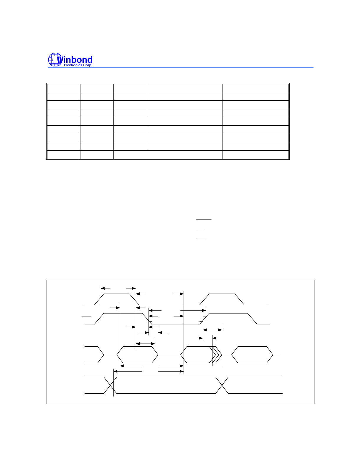
Preliminary W77C32
PSEN
RD
WR
M2 M1 M0 MOVX Cycles t
MCS
0 0 0 2 machine cycles 0
0 0 1 3 machine cycles 4 t
0 1 0 4 machine cycles 8 t
0 1 1 5 machine cycles 12 t
1 0 0 6 machine cycles 16 t
1 0 1 7 machine cycles 20 t
1 1 0 8 machine cycles 24 t
1 1 1 9 machine cycles 28 t
CLCL
CLCL
CLCL
CLCL
CLCL
CLCL
CLCL
Explanation of Logic Symbols
In order to maintain compatibility with the original 8051 family, this device specifies the same
parameter for each device, using the same symbols. The explanation of the symbols is as follows.
t Time A Address
C Clock D Input Data
H Logic level high L Logic level low
I Instruction P
Q Output Data R
V Valid W
signal
signal
X No longer a valid state Z Tri-state
TIMING WAVEFORMS
Program Memory Read Cycle
t
LHLL
ALE
t
AVLL
PSEN
PORT 0
PORT 2
ADDRESS
A0-A7
t
LLAX1
t
AVIV1
t
AVIV2
t
LLIV
t
t
LLPL
PLIV
t
PLPH
t
PLAZ
INSTRUCTION
- 66 -
t
PXIX
t
PXIZ
ADDRESS
IN
A0-A7
ADDRESS A8-A15ADDRESS A8-A15
Page 67
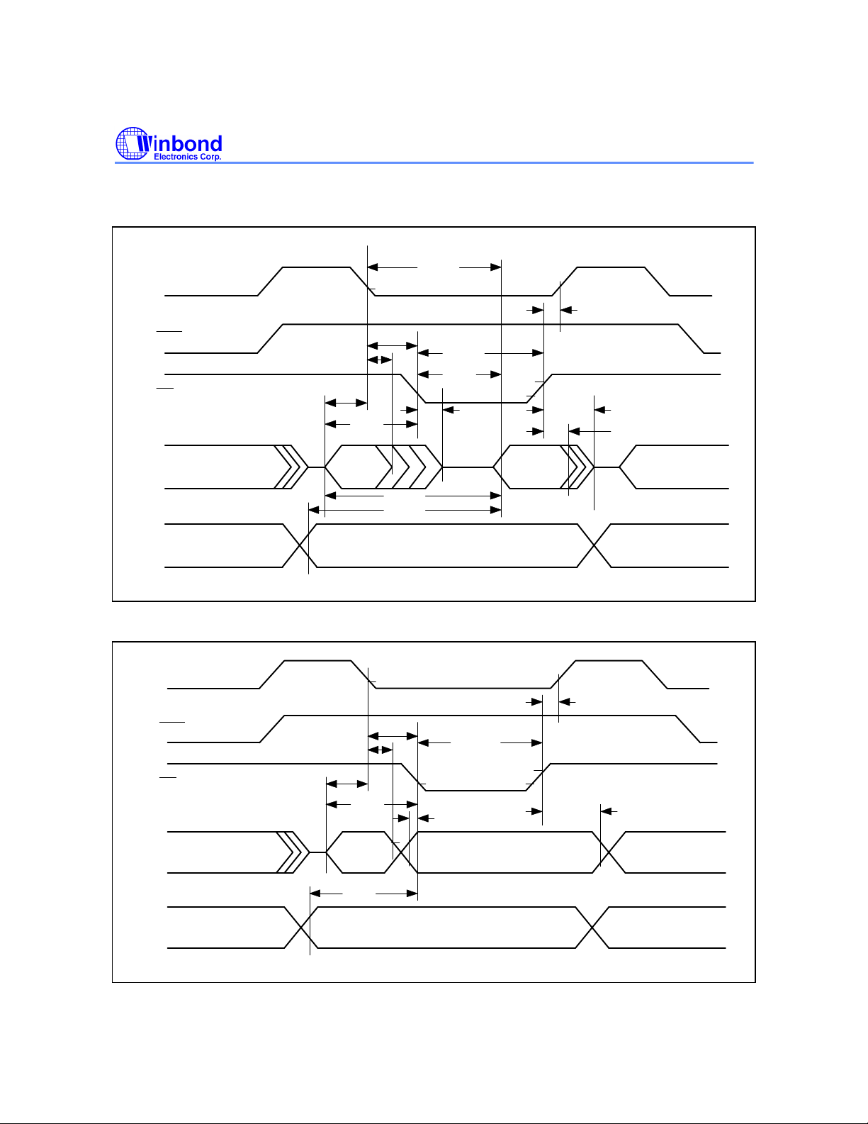
Timing Waveforms, continued
Data Memory Read Cycle
ALE
PSEN
RD
t
LLAX1
t
AVLL
t
AVWL1
t
LLWL
t
LLDV
t
RLRH
t
RLDV
t
RLAZ
Preliminary W77C32
t
WHLH
t
RHDZ
t
RHDX
PORT 0
PORT 2
INSTRUCTION
IN
Data Memory Write Cycle
ALE
PSEN
WR
PORT 0
INSTRUCTION
IN
ADDRESS
A0-A7
t
LLAX2
t
AVLL
t
ADDRESS
A0-A7
t
AVDV1
t
AVDV2
ADDRESS A8-A15
t
LLWL
AVWL1
t
QVWX
t
WLWH
DATA OUT
DATA
IN
t
WHQX
t
WHLH
ADDRESS
A0-A7
ADDRESS
A0-A7
PORT 2
t
AVDV2
ADDRESS A8-A15
Publication Release Date: March 1999
- 67 - Revision A1
Page 68
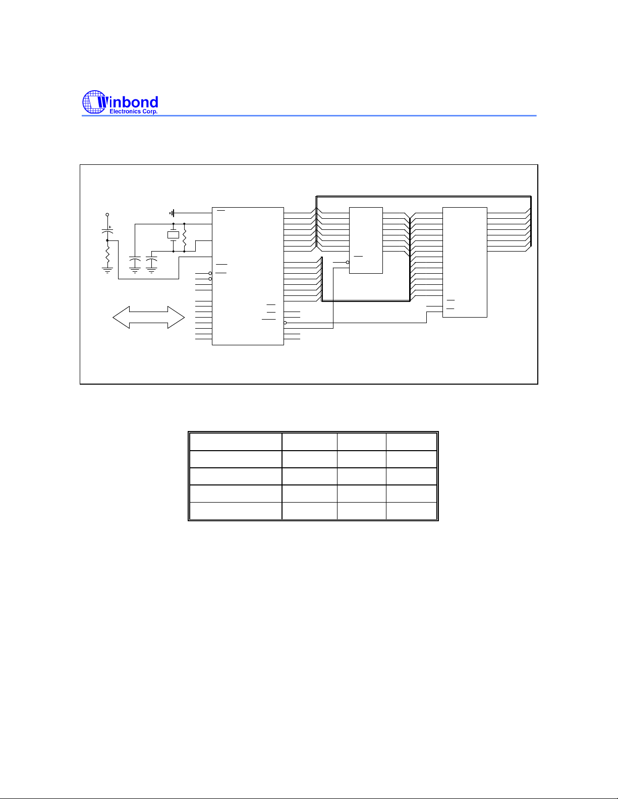
TYPICAL APPLICATION CIRCUITS
Expanded External Program Memory and Crystal
V
8.2 K
CC
10 u
CRYSTAL
C1
C2
31
EA
19
XTAL1
R
18
XTAL2
9
RST
INT0
12
13
INT1
14
T0
15
T1
1
P1.0
2
P1.1
3
P1.2
4
P1.3
5
P1.4
6
P1.5
7
P1.6
8
P1.7
W77C32
P0.0
P0.1
P0.2
P0.3
P0.4
P0.5
P0.6
P0.7
P2.0
P2.1
P2.2
P2.3
P2.4
P2.5
P2.6
P2.7
RD
WR
PSEN
ALE
TXD
RXD
AD0
39
38
37
36
35
34
33
32
21
22
23
24
25
26
27
28
17
16
29
30
11
10
AD1
AD2
AD3
AD4
AD5
AD6
AD7
A8
A9
A10
A11
A12
A13
A14
A15
AD0
AD1
AD2
AD3
AD4
AD5
AD6
AD7
GND
Preliminary W77C32
3
D0
4
D1
7
D2
8
D3
13
D4
14
D5
17
D6
18
D7
1
OC
11
G
74F373
2
Q0
5
Q1
6
Q2
9
Q3
12
Q4
15
Q5
16
Q6
19
Q7
A0
A0
A1
A2
A3
A4
A5
A6
A7
A10
A11
A12
A13
A14
A15
GND
10
A0
A1
9
A1
A2
8
A2
A3
7
A3
A4
6
A4
A5
5
A5
A6
4
A6
3
A7
A7
A8
25
A8
A9
24
A9
21
A10
23
A11
2
A12
26
A13
27
A14
1
A15
20
CE
22
OE
27512
11
O0
O1
O2
O3
O4
O5
O6
O7
AD0
12
AD1
13
AD2
15
AD3
16
AD4
17
AD5
18
AD6
19
AD7
CRYSTAL C1 C2 R
16 MHz 30P 30P 24 MHz 15P 15P 33 MHz 10P 10P 6.8K
40 MHz 1P 1P 2.4K
The above table shows the reference values for crystal applications.
Note: C1, C2, R components refer to Figure A.
Figure A
- 68 -
Page 69
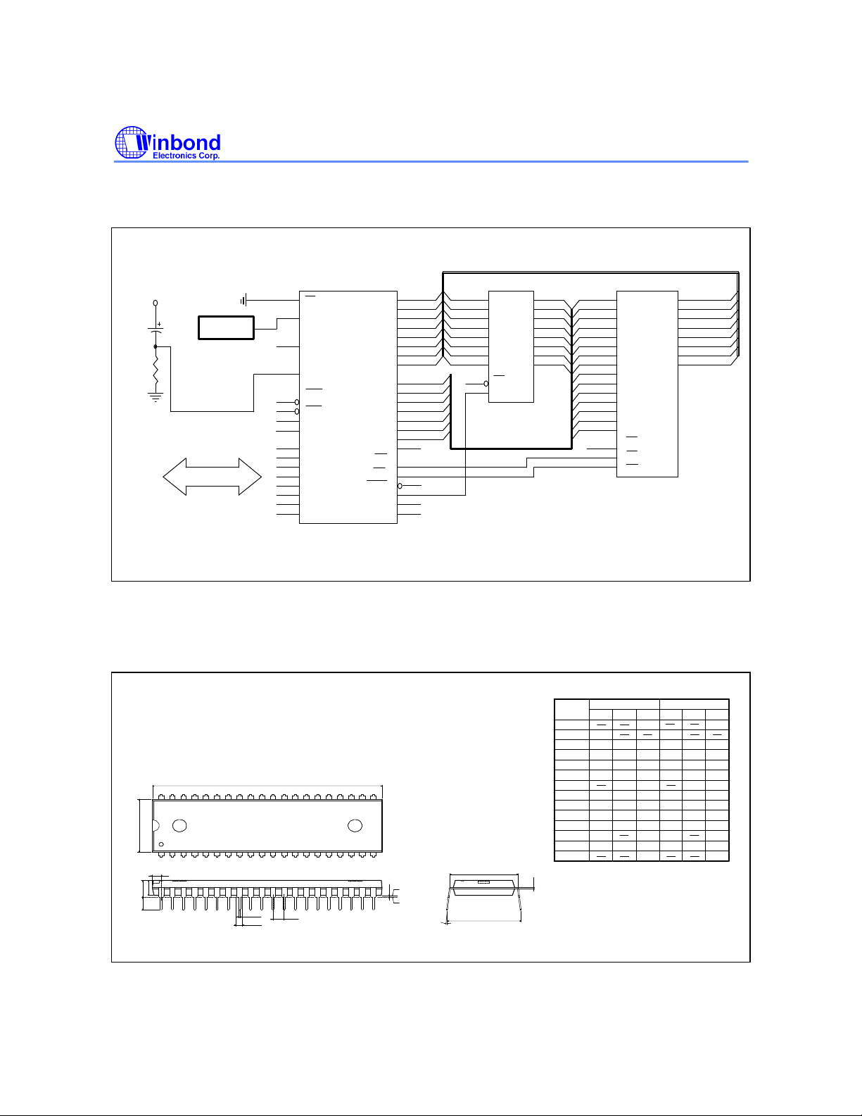
Typical Application Circuits, continued
Expanded External Data Memory and Oscillator
V
8.2 K
CC
10 u
OSCILLATOR
19
18
9
12
14
15
13
31
1
2
3
4
6
7
8
5
EA
XTAL1
XTAL2
RST
INT0
INT1
T0
T1
P1.0
P1.1
P1.2
P1.3
P1.4
P1.5
P1.6
P1.7
W77C32
P0.0
P0.1
P0.2
P0.3
P0.4
P0.5
P0.6
P0.7
P2.0
P2.1
P2.2
P2.3
P2.4
P2.5
P2.6
P2.7
RD
WR
PSEN
ALE
TXD
RXD
39
AD0
AD1
38
37
AD2
AD3
36
AD4
35
AD5
34
33
AD6
32
AD7
21
A8
22
A9
23
A10
24
A11
25
A12
26
A13
27
A14
28
17
16
29
30
11
10
AD0
AD1
AD2
AD3
AD4
AD5
AD6
AD7
GND
3
4
7
8
13
14
17
18
11
Preliminary W77C32
AD0
A0
2
D0
Q0
5
D1
Q1
6
D2
Q2
9
D3
Q3
12
D4
Q4
15
D5
Q5
16
D6
Q6
19
D7
OC
G
Q7
1
74F373
A0
10
A1
A1
A2
A2
A3
A3
A4
A4
A5
A5
A6
A6
A7
A7
A8
A9
A10
A11
A12
A13
A14
GND
A0
9
A1
8
A2
7
A3
6
A4
5
A5
4
A6
3
A7
25
A8
24
A9
21
A10
23
A11
2
A12
26
A13
1
A14
CE
20
22
OE
27
WR
20256
11
D0
D1
D2
D3
D4
D5
D6
D7
AD1
12
AD2
13
AD3
15
AD4
16
AD5
17
AD6
18
AD7
19
PACKAGE DIMENSIONS
40-pin DIP
40 21
1
E
1
S
2
A
A
L
D
B
1e
1B
Figure B
Dimension in inches Dimension in mm
Symbol
A
A
A
B
B 1
c
D
E
E
e
L
a
e
20
1
Base Plane
A
Seating Plane
E
A
e
a
S
Notes:
1. Dimension D Max. & S include mold flash or
tie bar burrs.
c
2. Dimension E1 does not include interlead flash.
3. Dimension D & E1 include mold mismatch and
are determined at the mold parting line.
4. Dimension B1 does not include dambar
protrusion/intrusion.
5. Controlling dimension: Inches.
6. General appearance spec. should be based on
final visual inspection spec.
1
2
1
1
A
Min.
0.010
0.150
0.016
0.008
0.540
0.120
0 15
Nom.
Max. Max.
0.210
0.155
0.160
0.018
0.022
0.050 1.27
0.0540.048
0.010
0.014
2.055 2.070
0.610
0.6000.590
0.5500.545
0.110
0.130
0.140
0.670
0.6500.630 16.00 16.51
0.090
.
Min.
0.254
3.81
0.406
0.203
14.986
13.72 13.9713.84
2.286 2.54 2.7940.090 0.100
3.048
Nom.
52.20
15.24
3.302
3.937
0.457
0.254
5.334
4.064
0.559
1.3721.219
0.356
52.58
15.494
3.556
17.01
150
2.286
Publication Release Date: March 1999
- 69 - Revision A1
Page 70
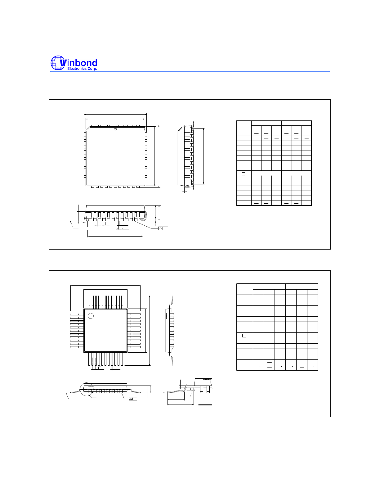
Package Dimensions, continued
44-pin PLCC
6 1
7
17
L
θ
Seating Plane
e
H
D
D
44 40
G
D
Preliminary W77C32
Dimension in inches Dimension in mm
Symbol
39
A
A
A
b
H
E
E
29
2818
A
2
A
b
b
1
A
1
y
G
E
c
b
c
D
E
e
G
G
H
H
L
y
Notes:
1. Dimension D & E do not include interlead
flash.
2. Dimension b1 does not include dambar
protrusion/intrusion.
3. Controlling dimension: Inches
4. General appearance spec. should be based
on final visual inspection spec.
Nom.
Min.
0.020
1
0.145
2
0.026
1
0.016
0.008
0.648
0.590
D
0.590
E
0.680
D
0.680
E
0.090
0.150
0.028
0.018
0.010
0.653
0.050 BSC
0.610
0.690
0.690
0.100
0.185
0.155
0.032
0.022
0.014
0.658
0.6580.6530.648
0.630
0.6300.610
0.700
0.110
0.004
Max. Max.
Min.
0.508
3.683
0.66
0.406
0.203
16.46
14.99
17.27
2.296
1.27
Nom.
3.81
0.711
0.457
0.254
16.59
15.49
15.4914.99
17.53
2.54
BSC
4.699
3.937
0.813
0.559
0.356
16.71
16.7116.5916.46
16.00
16.00
17.78
17.7817.5317.270.700
2.794
0.10
44-pin QFP
1
11
Seating Plane
H
D
D
44
12
e
34
33
E
EH
22
b
Notes:
c
A
A
See Detail F
2
1
A
y
θ
L
L 1
Detail F
Dimension in inch
Symbol
A
1
A
2
A
b
c
D
E
e
HD
E
H
L
1
L
y
θ
1. Dimension D & E do not include interlead
flash.
2. Dimension b does not include dambar
protrusion/intrusion.
3. Controlling dimension: Millimeter
4. General appearance spec. should be based
on final visual inspection spec.
Nom.
Min.
--- ---
0.002
0.01 0.02 0.25
0.081
0.075
0.01
0.014
0.006 0.152
0.394
0.390
0.390
0.025
0.031
0.510 13.45
0.520
0.520
0.510
0.025
0.031
0.063
0.051 0.075 1.295
0
Dimension in mm
Min.
--- ---
0.05
1.90
0.25
9.9
9.9
0.635
12.95
12.95
0.65
Nom.
0.5
2.05
2.20
0.45
0.35
0.2540.101
10.00
10.1
10.1
10.00
0.952
0.80
13.2
13.4513.2
0.8
0.95
1.6
1.905
0
0.08
Max. Max.
---
0.087
0.018
0.0100.004
0.398
0.3980.394
0.036
0.530
0.530
0.037
0.003
7
---
7
- 70 -
Page 71

Preliminary W77C32
Headquarters
No. 4, Creation Rd. III,
Science-Based Industrial Park,
Hsinchu, Taiwan
TEL: 886-3-5770066
FAX: 886-3-5792766
http://www.winbond.com.tw/
Voice & Fax-on-demand: 886-2-27197006
Winbond Electronics (H.K.) Ltd.
Rm. 803, World Trade Square, Tower II,
123 Hoi Bun Rd., Kwun Tong,
Kowloon, Hong Kong
TEL: 852-27513100
FAX: 852-27552064
Taipei Office
11F, No. 115, Sec. 3, Min-Sheng East Rd.,
Taipei, Taiwan
TEL: 886-2-27190505
FAX: 886-2-27197502
Note: All data and specifications are subject to change without notice.
Winbond Electronics North America Corp.
Winbond Memory Lab.
Winbond Microelectronics Corp.
Winbond Systems Lab.
2727 N. First Street, San Jose,
CA 95134, U.S.A.
TEL: 408-9436666
FAX: 408-5441798
Publication Release Date: March 1999
- 71 - Revision A1
 Loading...