

Page 1

W49F102
64K × 16 CMOS FLASH MEMORY
GENERAL DESCRIPTION
The W49F102 is a 1-megabit, 5-volt only CMOS flash memory organized as 64K × 16 bits. The device
can be programmed and erased in-system with a standard 5V power supply. A 12-volt VPP is not
required. The unique cell architecture of the W49F102 results in fast program/erase operations with
extremely low current consumption (compared to other comparable 5-volt flash memory products). The
device can also be programmed and erased using standard EPROM programmers.
FEATURES
• Single 5-volt operations:
− 5-volt Read
− 5-volt Erase
− 5-volt Program
• Fast Program operation:
− Word-by-Word programming: 50 µS (max.)
• Fast Erase operation: 100 mS (typ.)
• Fast Read access time: 40/45 nS
• Endurance: 10K cycles (typ.)
• Ten-year data retention
• Hardware data protection
• 8K word Boot Block with Lockout protection
• Low power consumption
− Active current: 25 mA (typ.)
− Standby current: 20 µA (typ.)
• Automatic program and erase timing with
internal VPP generation
• End of program or erase detection
− Toggle bit
− Data polling
• Latched address and data
• TTL compatible I/O
• JEDEC standard word-wide pinouts
• Available packages: 40-pin TSOP and 44-pin
PLCC
Publication Release Date: October 2000
- 1 - Revision A3
Page 2
W49F102
CE
OE
WE
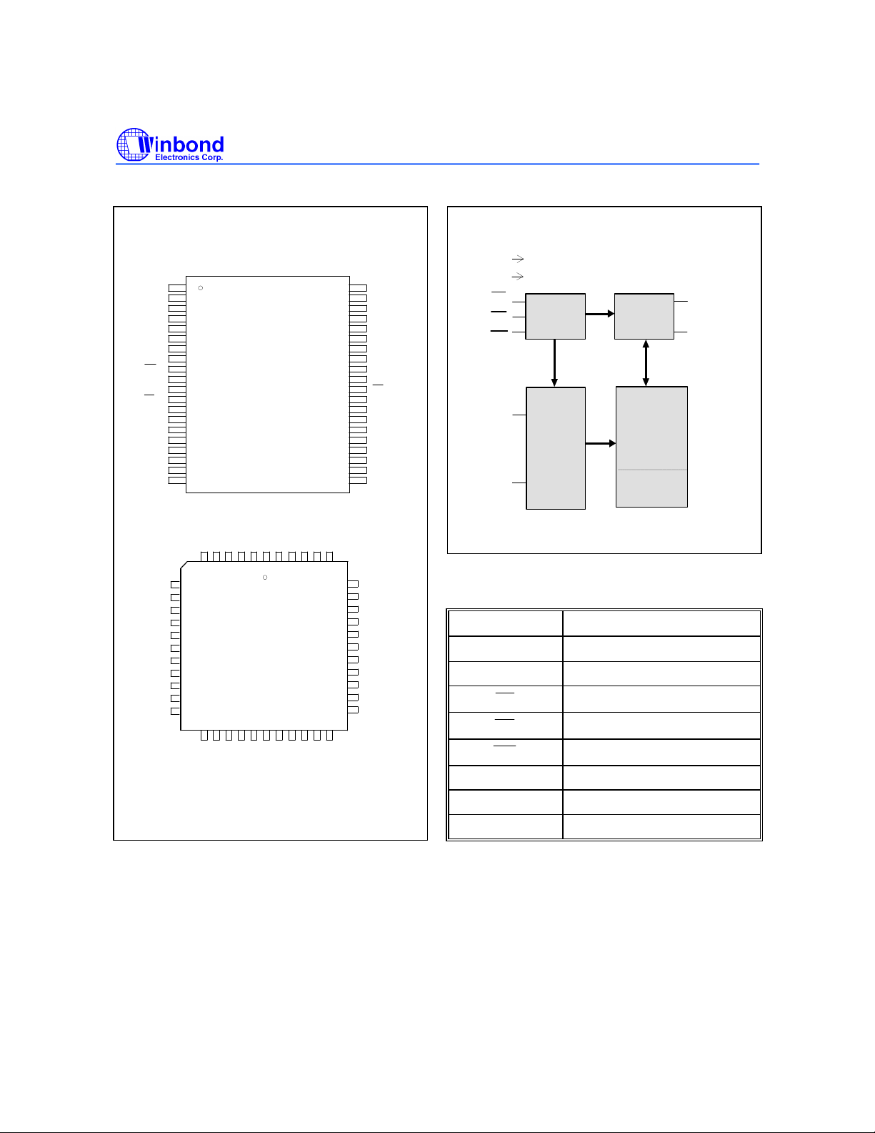
PIN CONFIGURATIONS
A9
A10
A11
A12
A13
A14
A15
NC
WE
V
NC
CE
DQ15
DQ14
DQ13
DQ12
DQ11
DQ10
DQ9
DQ8
DQ12
DQ11
DQ10
DD
DQ9
DQ8
Vss
DQ7
DQ6
DQ5
DQ4
1
2
3
4
5
6
7
8
9
10
11
12
13
14
15
16
17
18
19
20
D
Q
13
6
7
8
9
10
11
12
13
NC
14
15
16
17
18
D
Q
3
40-pin
TSOP
D
C
Q
Q
E
15
14
5
3
4
/
D
N
W
N
D
C
E
C
441
43
2
V
/
D
44-pin
PLCC
23
20
22
24
21
19
D
Q
2
N
D
Q
1
A
/
D
Q
0
A1A
C
O
0
E
BLOCK DIAGRAM
V
DD
V
40
Vss
39
A8
38
A7
37
A6
36
A5
35
A4
34
A3
33
A2
32
A1
A0
31
30
OE
29
DQ0
28
DQ1
27
DQ2
26
DQ3
25
DQ4
DQ5
24
DQ6
23
DQ7
22
Vss
21
A
A
1
1
N
4
5
C
4041
42
39
A13
38
A12
37
A11
36
A10
35
A9
34
Vss
33
NC
32
A8
31
A7
30
A6
29
27
2625
A
3
2
A5
28
A
4
PIN DESCRIPTION
SS
CE
OE
WE
A0
.
.
A15
CONTROL
DECODER
OUTPUT
BUFFER
MAIN
MEMORY
(56K Words)
BootBlock
(8K Words)
DQ0
.
.
DQ15
SYMBOL PIN NAME
A0 - A15
Address Inputs
DQ0 - DQ15 Data Inputs/Outputs
Chip Enable
Output Enable
Write Enable
VDD Power Supply
Vss Ground
NC No Connection
- 2 -
Page 3

W49F102
FUNCTIONAL DESCRIPTION
Read Mode
The read operation of the W49F102 is controlled by CE and OE, both of which have to be low for
the host to obtain data from the outputs. CE is used for device selection. When CE is high, the
chip is de-selected and only standby power will be consumed. OE is the output control and is used
to gate data from the output pins. The data bus is in high impedance state when either CE or OE
is high. Refer to the timing waveforms for further details.
Boot Block Operation
There is one 8K-word boot block in this device, which can be used to store boot code. It is located in
the first 8K words of the memory with the address range from 0000 hex to 1FFF hex.
See Command Codes for Boot Block Lockout Enable for the specific code. Once this feature is set the
data for the designated block cannot be erased or programmed (programming lockout); other memory
locations can be changed by the regular programming method. Once the boot block programming
lockout feature is activated, the chip erase function will only affect the main memory.
In order to detect whether the boot block feature is set on the 8K-words block, users can perform
software command sequence: enter the product identification mode (see Command Codes for
Identification/Boot Block Lockout Detection for specific code), and then read from address "0002 hex".
If the output data is "FF hex," the boot block programming lockout feature is activated; if the output
data is "FE hex," the lockout feature is inactivated and the block can be erased/programmed.
To return to normal operation, perform a three-byte command sequence (or an alternate single-word
command) to exit the identification mode. For the specific code, see Command Codes for
Identification/Boot Block Lockout Detection.
Chip Erase Operation
The chip-erase mode can be initiated by a six-word command sequence. After the command loading
cycle, the device enters the internal chip erase mode, which is automatically timed and will be
completed in a fast 100 mS (typical). The host system is not required to provide any control or timing
during this operation. If the boot block programming lockout is activated, only the data in the main
memory will be erased to FF(hex), and the data in the boot block will not be erased (remains same as
before the chip erase operation). The entire memory array (main memory and boot block) will be
erased to FF(hex). by the chip erase operation if the boot block programming lockout feature is not
activated. The device will automatically return to normal read mode after the erase operation
completed. Data polling and/or Toggle Bits can be used to detect end of erase cycle.
Main Memory Erase Operation
The main memory erase mode can be initiated by a six-word command sequence. After the command
loading cycle, the device enters the internal main-memory erase mode, which is automatically timed
and will be completed in a fast 100 mS (typical). The host system is not required to provide any control
or timing during this operation. The device will automatically return to normal read mode after the erase
operation completed. Data polling and/or Toggle Bits can be used to detect end of erase cycle.
Publication Release Date: October 2000
- 3 - Revision A3
Page 4

W49F102
WE
Program Operation
The W49F102 is programmed on a word-by-word basis. Program operation can only change logical
data "1" to logical data "0" The erase operation (changed entire data in main memory and/or boot block
from "0" to "1" is needed before programming.
The program operation is initiated by a 4-word command cycle (see Command Codes for Word
Programming). The device will internally enter the program operation immediately after the wordprogram command is entered. The internal program timer will automatically time-out (50 µS max. TBP) once completed and return to normal read mode. Data polling and/or Toggle Bits can be used to
detect end of program cycle.
Hardware Data Protection
The integrity of the data stored in the W49F102 is also hardware protected in the following ways:
(1) Noise/Glitch Protection: A WE pulse of less than 15 nS in duration will not initiate a write cycle.
(2) VDD Power Up/Down Detection: The programming operation is inhibited when VDD is less than
2.5V typical.
(3) Write Inhibit Mode: Forcing OE low, CE high, or WE high will inhibit the write operation.
This prevents inadvertent writes during power-up or power-down periods.
(4) VDD power-on delay: When VDD has reached its sense level, the device will automatically time-out
5 mS before any write (erase/program) operation.
Data Polling (DQ7 & DQ15)- Write Status Detection
The W49F102 includes a data polling feature to indicate the end of a program or erase cycle.
When the W49F102 is in the internal program or erase cycle, any attempt to read DQ7 or DQ15 of the
last word loaded will receive the complement of the true data. Once the program or erase cycle is
completed, DQ7 or DQ15 will show the true data. Note that DQ7 or DQ15 will show logical "0" during the
erase cycle, and become logical "1" or true data when the erase cycle has been completed.
Toggle Bit (DQ6 & DQ14)- Write Status Detection
In addition to data polling, the W49F102 provides another method for determining the end of a
program cycle. During the internal program or erase cycle, any consecutive attempts to read DQ6 or
DQ14 will produce alternating 0's and 1's. When the program or erase cycle is completed, this toggling
between 0's and 1's will stop. The device is then ready for the next operation.
Product Identification
The product ID operation outputs the manufacturer code and device code. Programming equipment
automatically matches the device with its proper erase and programming algorithms.
The manufacturer and device codes can be accessed by software or hardware operation. In the
software access mode, a six-word (or JEDEC 3-word) command sequence can be used to access the
product ID. A read from address 0000H outputs the manufacturer code (00DAh). A read from address
0001H outputs the device code (002Fh). The product ID operation can be terminated by a three-word
command sequence or an alternate one-word command sequence (see Command Definition table).
In the hardware access mode, access to the product ID is activated by forcing CE and OE low,
high, and raising A9 to 12 volts.
- 4 -
Page 5
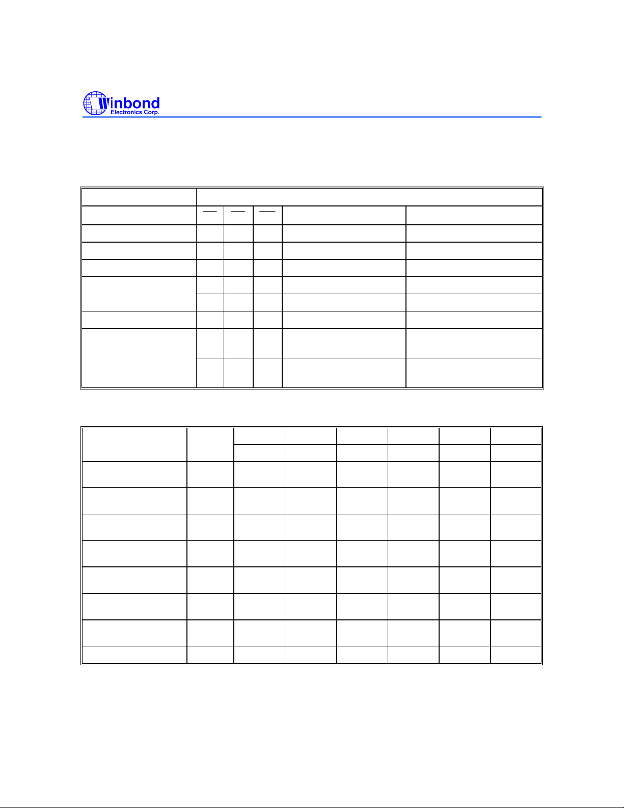
TABLE OF OPERATING MODES
CE OE WE
5555
2AAA
5555
5555
2AAA
5555
5555
2AAA
5555
5555
2AAA
5555
5555
2AAA
5555
5555
2AAA
5555
5555
2AAA
5555
5555
2AAA
5555
5555
2AAA
5555
Operating Mode Selection
(VHH = 12V ± 5%)
MODE PINS
W49F102
ADDRESS DQ.
Read VIL VIL VIH AIN Dout
Write VIL VIH VIL AIN Din
Standby VIH X X X High Z
Write Inhibit X VIL X X High Z/DOUT
X X VIH X High Z/DOUT
Output Disable X VIH X X High Z
Product ID VIL VIL VIH
VIL VIL VIH
A0 = VIL; A1−A15 = VIL;
A9 = VHH
A0 = VIH; A1−A15 = VIL;
A9 = VHH
Manufacturer Code 00DA
(Hex)
Device Code
002F (Hex)
TABLE OF COMMAND DEFINITION
Command No. of 1st Cycle 2nd Cycle 3rd Cycle 4th Cycle 5th Cycle 6th Cycle
Description Cycles
Read 1
Chip Erase 6
Main Memory Erase 6
Word Program 4
Boot Block Lockout 6
Product ID Entry 3
Product ID Exit
Product ID Exit
(1)
3
(1)
1
Addr. Data Addr. Data Addr. Data Addr. Data Addr. Data Addr. Data
A
D
OUT
AA
AA
AA
AA
IN
55
55
55
55
80
80
A0
80
AA
AA
A
IN
DIN
AA
55
55
55
AA
55
90
AA
XXXX F0
55
F0
10
30
40
Note: Address Format: A14−A0 (Hex); Data Format: DQ15−DQ8 (Don't Care); DQ7-DQ0 (Hex)
Either one of the two Product ID Exit commands can be used.
Publication Release Date: October 2000
- 5 - Revision A3
Page 6
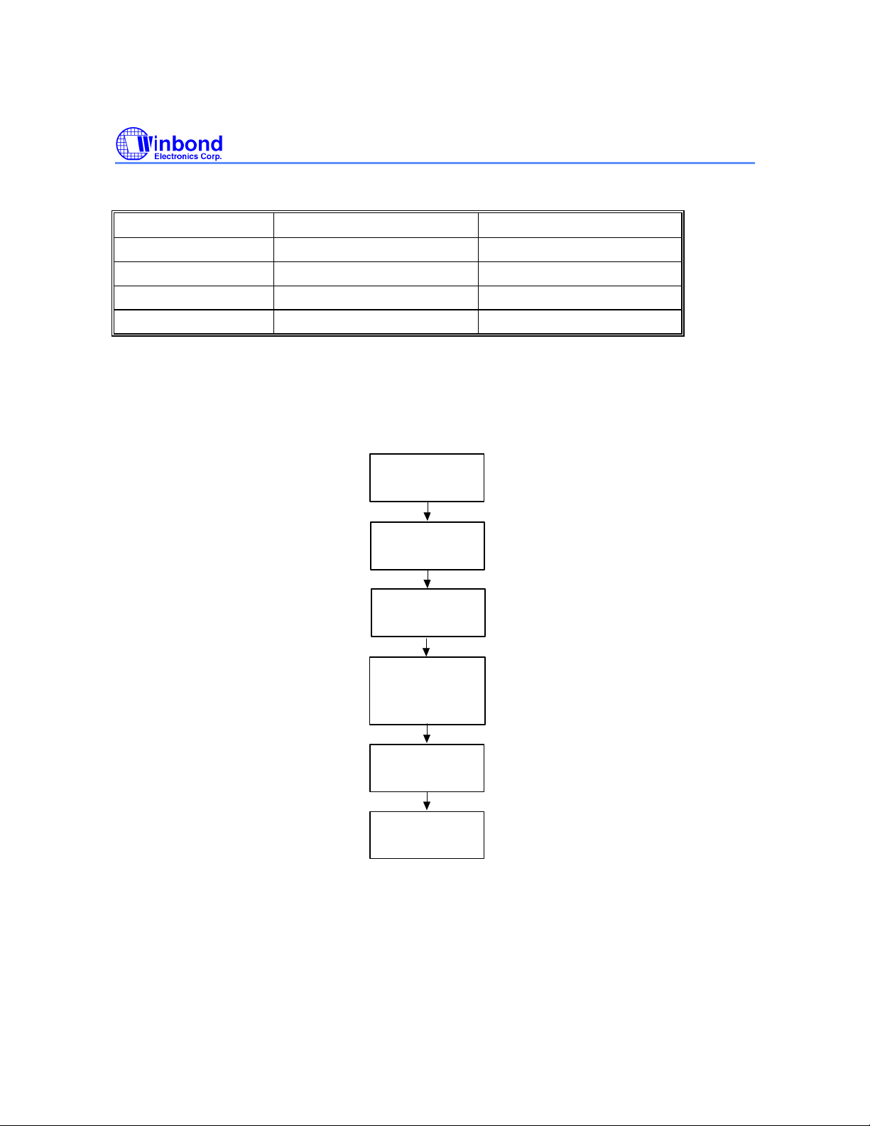
Command Codes for Word Program
Command Flow
WORD SEQUENCE ADDRESS DATA
0 Write 5555H AAH
1 Write 2AAAH 55H
2 Write 5555H A0H
3 Write Programmed-Address Programmed-Data
Word Program Flow Chart
Word Program
Load data AA
to
address 5555
W49F102
Notes for software program code:
Data Format: DQ15−DQ0 (Hex); XX = Don't Care
Address Format: A14−A0 (Hex)
Load data 55
to
address 2AAA
Load data A0
to
address 5555
Load data Din
to
programmed-
address
Pause 50 S
µ
Exit
- 6 -
Page 7
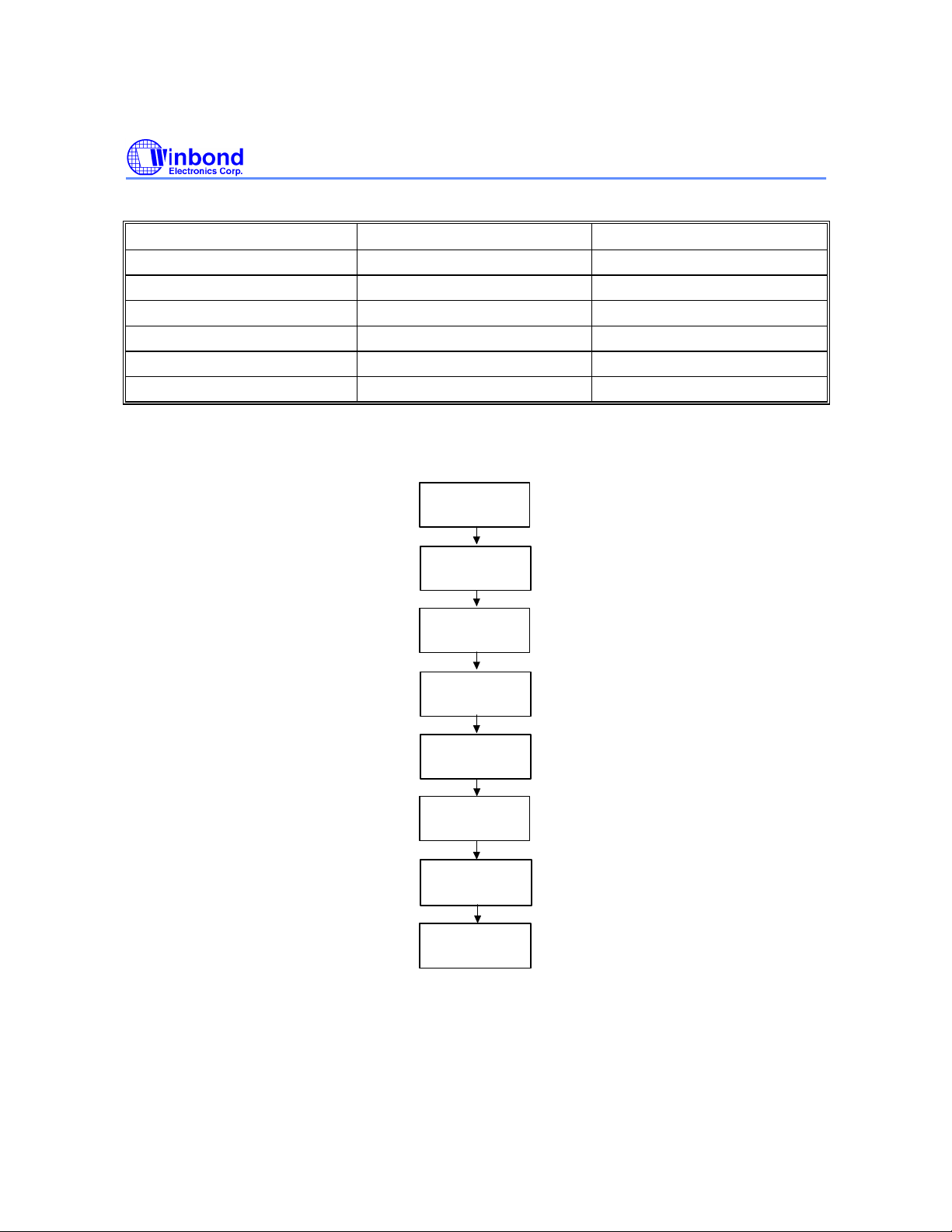
Command Codes for Chip Erase
55H
10H
BYTE SEQUENCE ADDRESS DATA
1 Write 5555H AAH
2 Write 2AAAH
3 Write 5555H 80H
4 Write 5555H AAH
5 Write 2AAAH 55H
6 Write 5555H
Chip Erase Acquisition Flow
Load data AA
to
address 5555
Load data 55
to
address 2AAA
W49F102
Notes for chip erase:
Data Format: DQ15-DQ8: Don't Care; DQ7−DQ0 (Hex)
Address Format: A14−A0 (Hex)
Load data 80
to
address 5555
Load data AA
to
address 5555
Load data 55
to
address 2AAA
Load data 10
to
address 5555
Pause 1 Sec.
Exit
Publication Release Date: October 2000
- 7 - Revision A3
Page 8
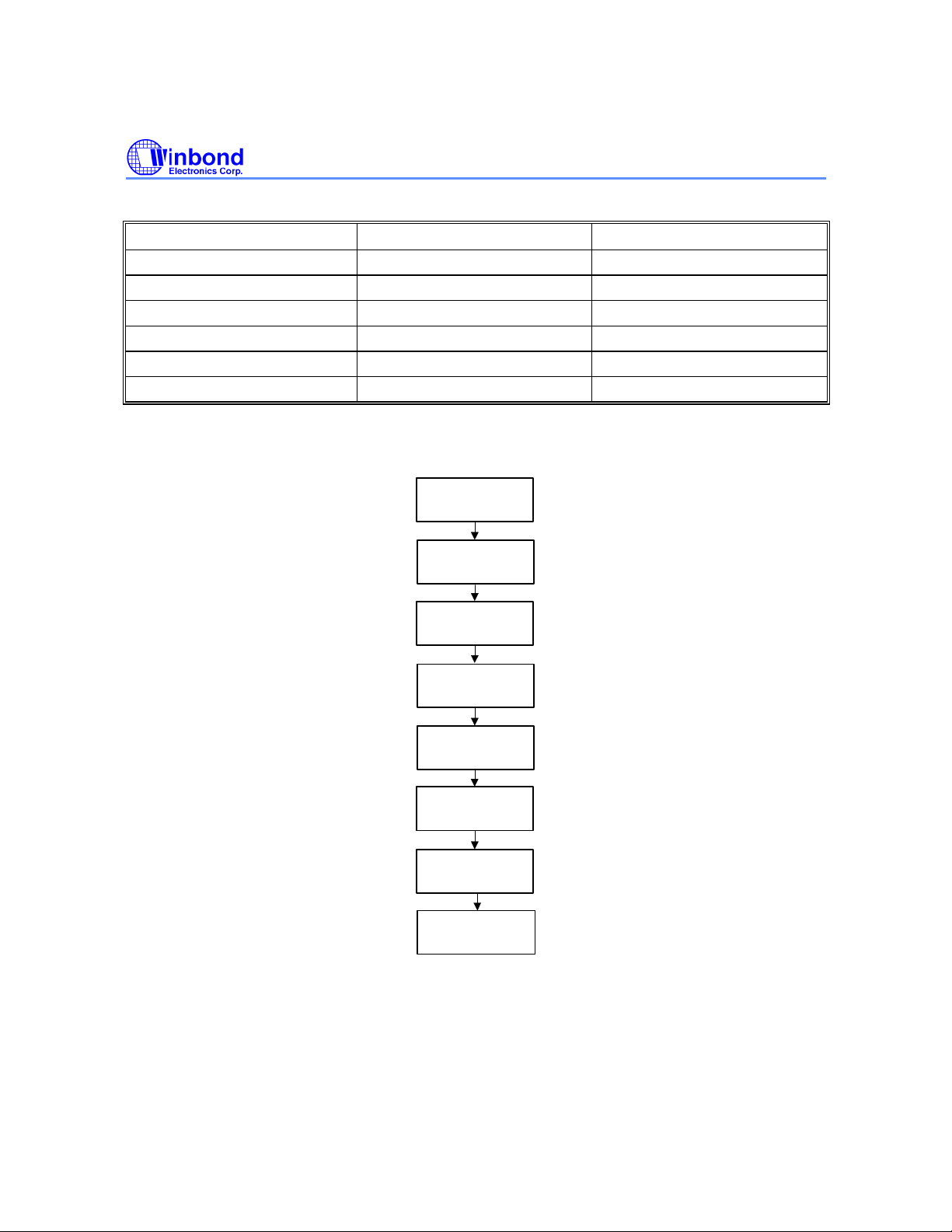
Command Codes for Main Memory Erase
55H
30H
BYTE SEQUENCE ADDRESS DATA
1 Write 5555H AAH
2 Write 2AAAH
3 Write 5555H 80H
4 Write 5555H AAH
5 Write 2AAAH 55H
6 Write 5555H
Main Memory Erase Acquisition Flow
Load data AA
address 5555
Load data 55
address 2AAA
W49F102
to
to
Notes for chip erase:
Data Format: DQ15-DQ8: Don't Care; DQ7−DQ0 (Hex)
Address Format: A14−A0 (Hex)
Load data 80
to
address 5555
Load data AA
to
address 5555
Load data 55
to
address 2AAA
Load data 30
to
address 5555
Pause 1 Sec.
Exit
- 8 -
Page 9
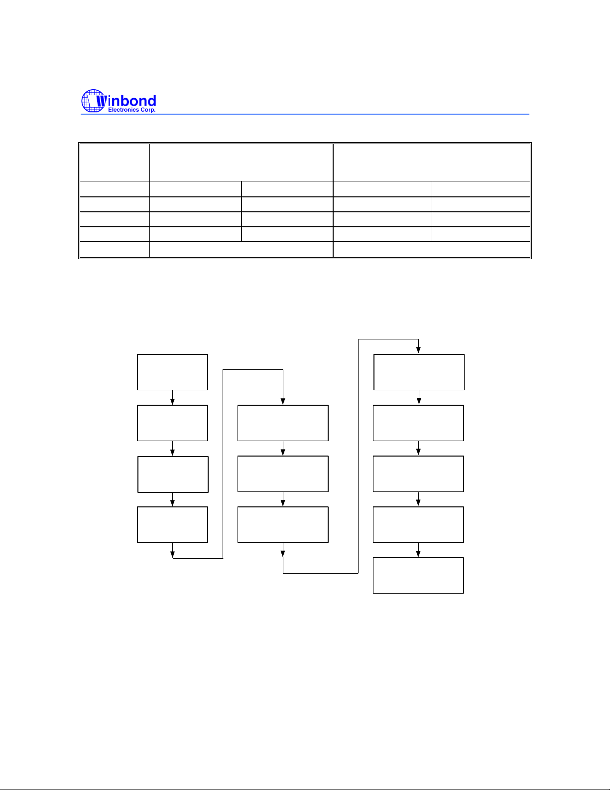
W49F102
(5)
Command Codes for Product Identification and Boot Block Lockout Detection
BYTE
SEQUENCE
PRODUCT IDENTIFICATION/BOOT
BLOCK LOCKOUT DETECTION ENTRY
IDENTIFICATION/BOOT BLOCK LOCKOUT
ADDRESS DATA ADDRESS DATA
1 Write 5555 AA 5555H AAH
2 Write 2AAA 55 2AAAH 55H
3 Write 5555 90 5555H F0H
Pause 10 µS Pause 10 µS
SOFTWARE PRODUCT
DETECTION EXIT (6)
Software Product Identification and Boot Block Lockout Detection Acquisition Flow
Product
Identification
Entry (1)
Load data AA
to
address 5555
Load data 55
to
address 2AAA
Product
Identification
and Boot Block
Lockout Detection
Mode (3)
Read address = 00000
data = DA
(2)
Product
Identification Exit (6)
Load data AA
to
address 5555
Load data 55
to
address 2AAA
Load data 90
to
address 5555
Pause 10 S
µ
Read address = 00001
data = 2F
Read address = 00002
data = FF/FE
(2)
(4)
Load data F0
to
address 5555
Pause 10 S
Normal Mode
µ
Notes for software product identification/boot block lockout detection:
(1) Data Format: DQ15-DQ8 (Don't Care), DQ7−DQ0 (Hex); Address Format: A14−A0 (Hex)
(2) A1−A15 = VIL; manufacture code is read for A0 = VIL; device code is read for A0 = VIH.
(3) The device does not remain in identification and boot block lockout detection mode if power down.
(4) If the output data is "FF Hex," the boot block programming lockout feature is activated; if the output data "FE Hex," the lockout feature is
inactivated and the block can be programmed.
(5) The device returns to standard operation mode.
(6) Optional 1-write cycle (write F0 hex at XXXX address) can be used to exit the product identification/boot block lockout detection.
Publication Release Date: October 2000
- 9 - Revision A3
Page 10
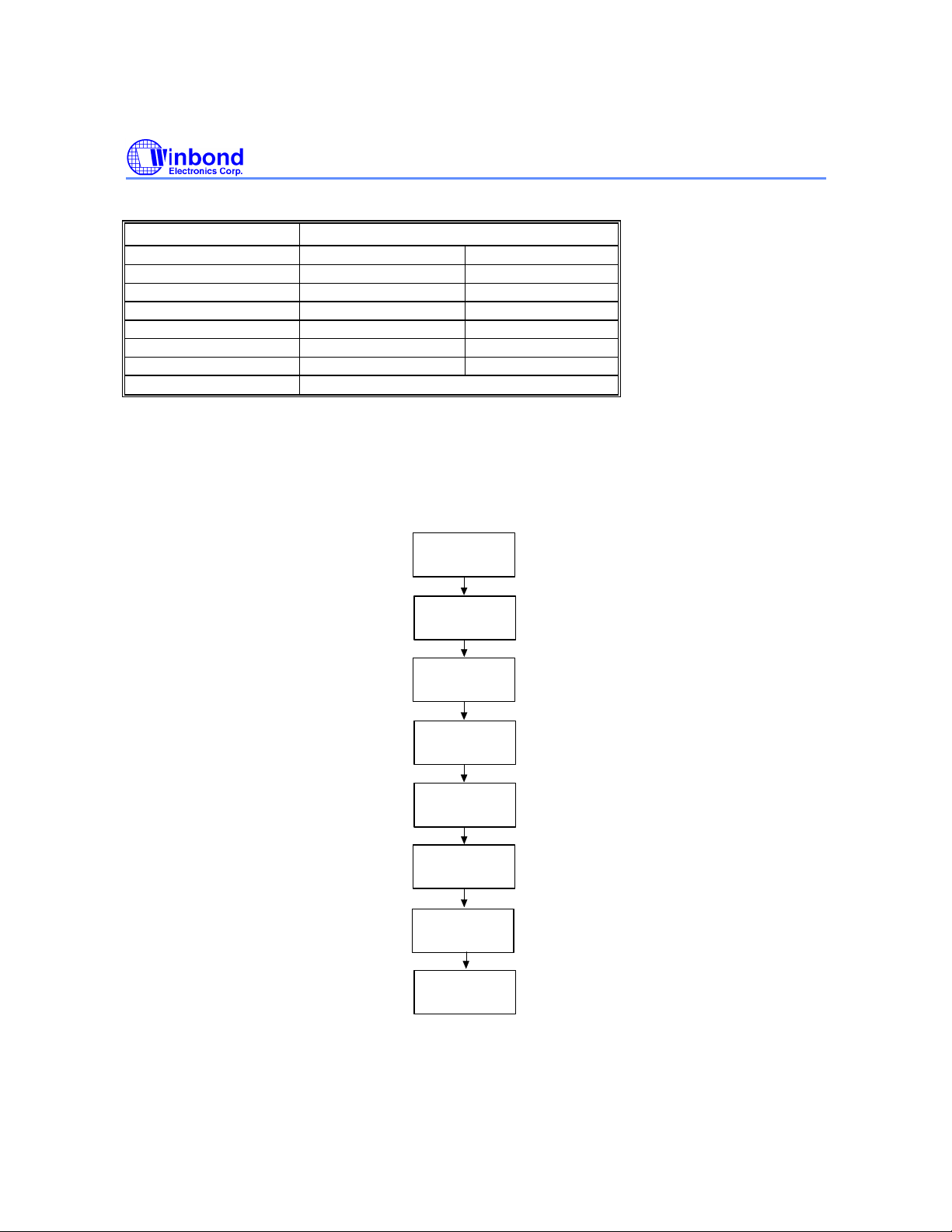
Command Codes for Boot Block Lockout Enable
BYTE SEQUENCE BOOT BLOCK LOCKOUT FEATURE SET
ADDRESS DATA
1 Write 5555H AAH
2 Write 2AAAH 55H
3 Write 5555H 80H
4 Write 5555H AAH
5 Write 2AAAH 55H
6 Write 5555H 40H
Pause 1 Sec.
Boot Block Lockout Enable Acquisition Flow
Boot Block Lockout
Feature Set Flow
Load data AA
to
address 5555
W49F102
address 2AAA
address 5555
address 5555
address 2AAA
address 5555
Pause 1 Sec.
Notes for boot block lockout enable:
Data Format: DQ15-DQ8 Don't Care), DQ7−DQ0 (Hex)
Address Format: A14−A0 (Hex)
Load data 55
to
Load data 80
to
Load data AA
to
Load data 55
to
Load data 40
to
Exit
- 10 -
Page 11
W49F102
CE
mA
CE
CE
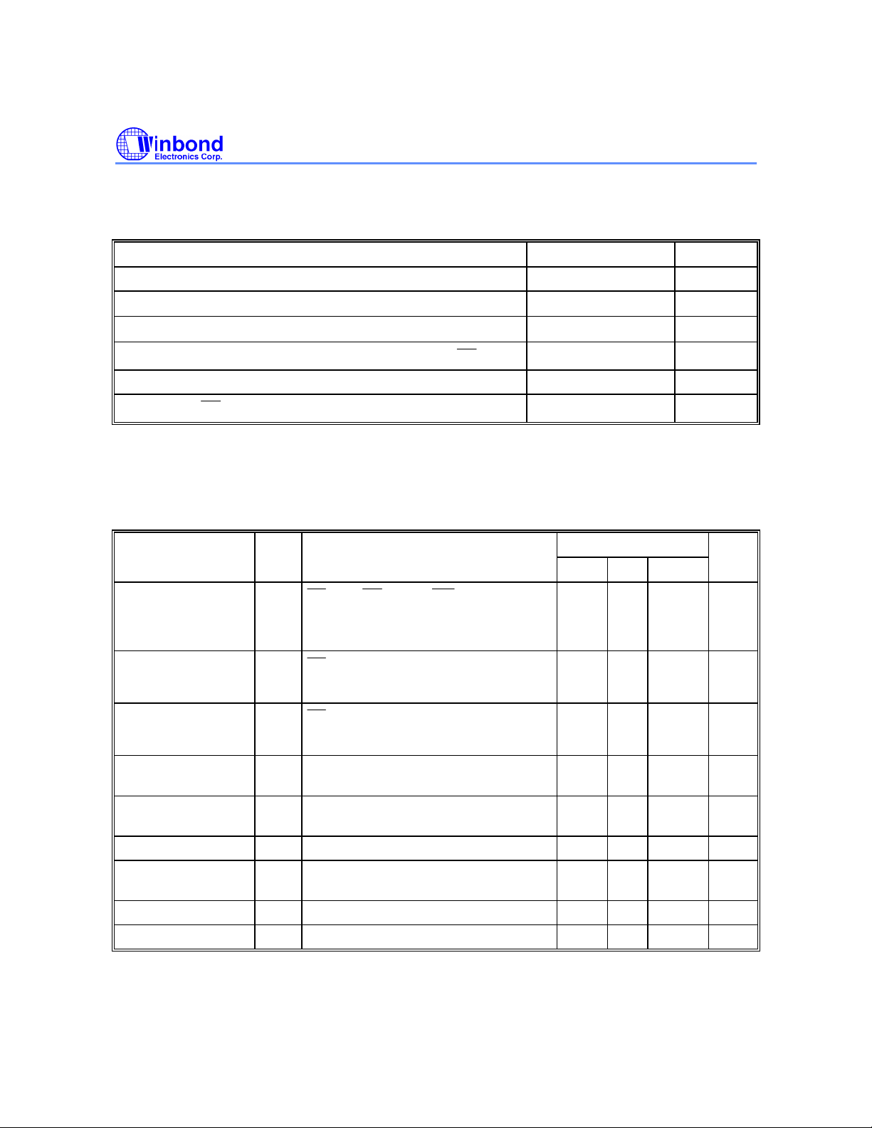
DC CHARACTERISTICS
Absolute Maximum Ratings
PARAMETER RATING UNIT
Power Supply Voltage to VSS Potential -0.5 to +7.0 V
Operating Temperature 0 to +70
Storage Temperature -65 to +150
D.C. Voltage on Any Pin to Ground Potential except OE
Transient Voltage (<20 nS ) on Any Pin to Ground Potential -1.0 to VDD +1.0 V
Voltage on OE Pin to Ground Potential
Note: Exposure to conditions beyond those listed under Absolute Maximum Ratings may adversely affect the life and reliability
of the device.
-0.5 to VDD +1.0 V
-0.5 to 12.5 V
°C
°C
DC Operating Characteristics
(VDD = 5.0V ±10%, VSS = 0V, TA = 0 to 70° C)
PARAMETER SYM.
MIN. TYP. MAX.
Power Supply
Current
Standby VDD
Current (TTL input)
Standby VDD Current
(CMOS input)
Input Leakage
Current
Output Leakage
Current
Input Low Voltage VIL - -0.3
Input High Voltage VIH
Output Low Voltage VOL IOL = 2.1 mA - - 0.45 V
Output High Voltage VOH IOH = -0.4 mA 2.4 - - V
ICC
all I/Os open
Address inputs = VIL/VIH, at f = 5 MHz
ISB1
Other inputs = VIL/VIH
ISB2
Other inputs = VDD -0.3V/Vss
ILI VIN = Vss to VDD - - 10
ILO VOUT = Vss to VDD - - 10
TEST CONDITIONS LIMITS UNIT
= OE= VIL, WE = VIH,
= VIH, all I/Os open
= VDD -0.3V, all I/Os open
- 2.0 - VDD
- 25
- 2 3 mA
- 20
- 0.8 V
50
100
+0.5
µA
µA
µA
V
Publication Release Date: October 2000
- 11 - Revision A3
Page 12
W49F102
Power-up Timing
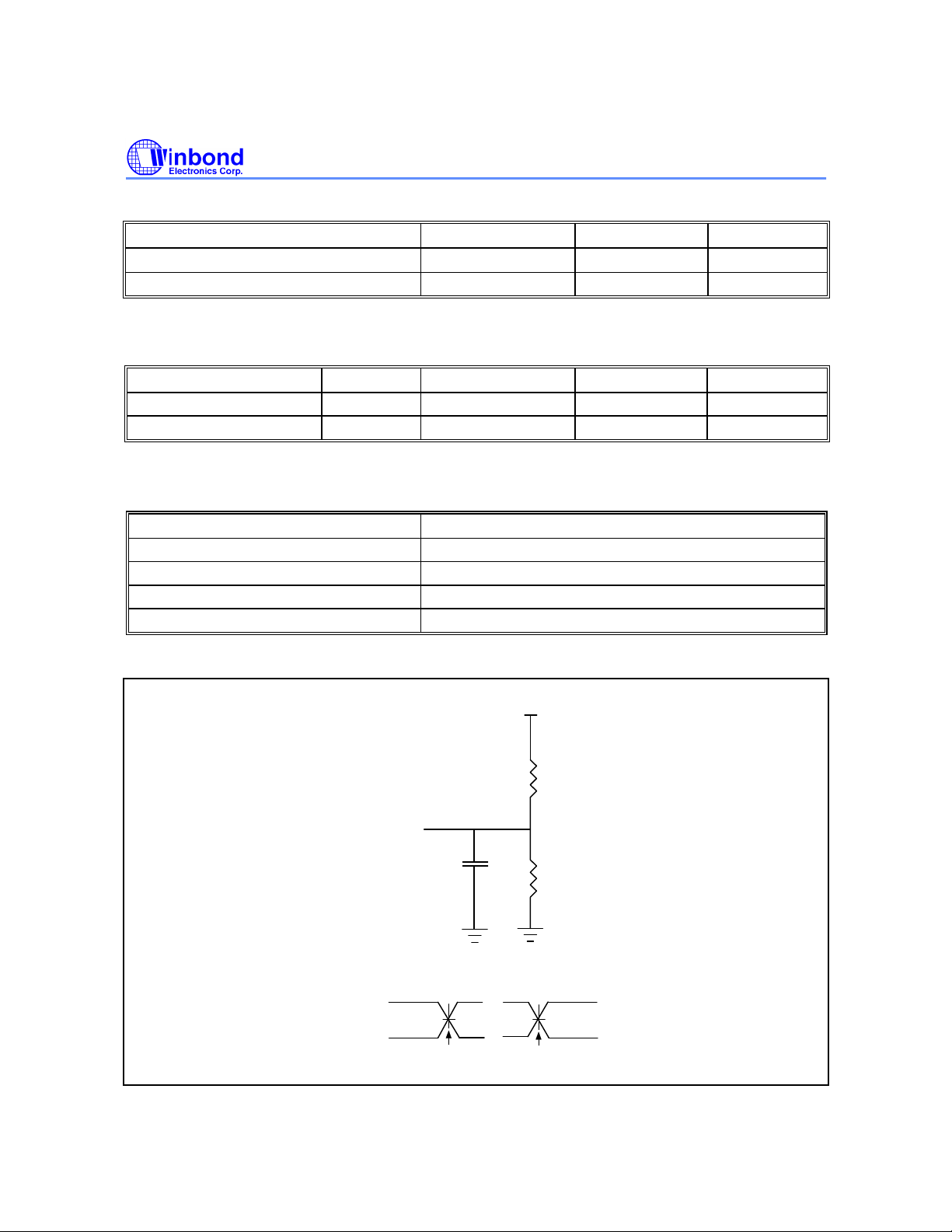
PARAMETER SYMBOL TYPICAL UNIT
Power-up to Read Operation TPU. READ 100
Power-up to Write Operation TPU. WRITE 5 mS
CAPACITANCE
(VDD = 5.0V, TA = 25° C, f = 1 MHz)
PARAMETER SYMBOL CONDITIONS MAX. UNIT
I/O Pin Capacitance CI/O VI/O = 0V 12 pf
Input Capacitance CIN VIN = 0V 6 pf
AC CHARACTERISTICS
AC Test Conditions
PARAMETER CONDITIONS
Input Pulse Levels 0V to 3.0V
Input Rise/Fall Time <5 nS
Input/Output Timing Level 1.5V/1.5V
Output Load 1 TTL Gate and CL = 30 pF
µS
AC Test Load and Waveform
Input
D
OUT
(Including Jig and
3V
0V
30 pF
Scope)
Test Point
1.5V
+5V
Output
1.5V
Test Point
1.8K
1.3K
Ω
Ω
- 12 -
Page 13
CE
OE
CE
OE
W49F102
AC Characteristics, continued
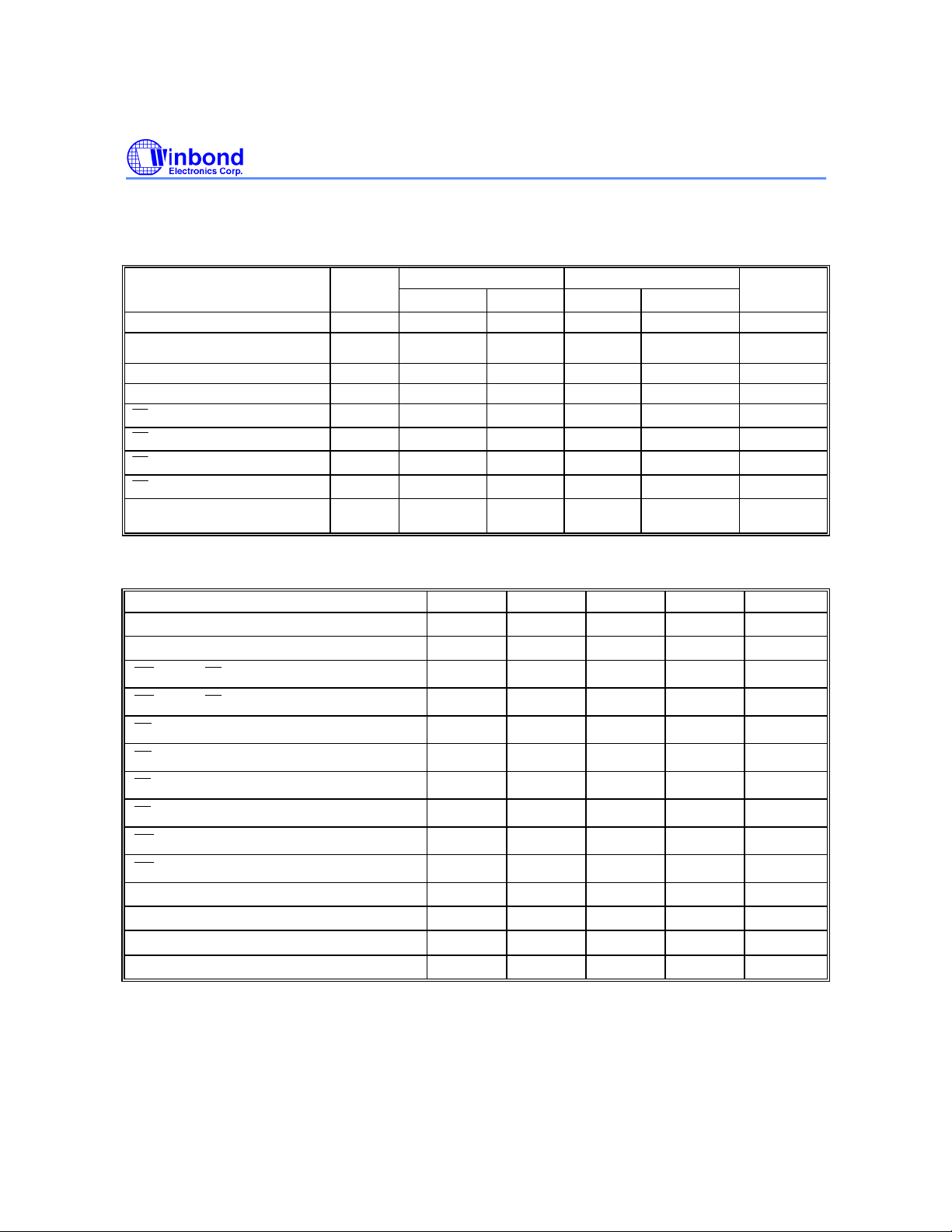
Read Cycle Timing Parameters
(VDD = 5.0V ±5 % for 35 nS; VDD = 5.0V ±10 % for 40/45 nS, VSS = 0V, TA = 0 to 70° C)
PARAMETER SYM. W49F102-40 W49F102-45 UNIT
Read Cycle Time TRC 42 - 45 - nS
Chip Enable Access Time TCE - 40 - 45 nS
Address Access Time TAA - 40 - 45 nS
Output Enable Access Time TOE - 20 - 25 nS
Low to Active Output
Low to Active Output
High to High-Z Output
High to High-Z Output
Output Hold from Address
Change
TCLZ 0 - 0 - nS
TOLZ 0 - 0 - nS
TCHZ - 15 - 20 nS
TOHZ - 15 - 20 nS
TOH 0 - 0 - nS
Write Cycle Timing Parameters
PARAMETER SYMBOL
Address Setup Time TAS 0
Address Hold Time TAH 45
and CE Setup Time
WE
WE and CE Hold Time
High Setup Time
OE
OE High Hold Time
CE Pulse Width
CE High Width
WE Pulse Width
High Width
WE
Data Setup Time TDS 45
Data Hold Time TDH 0
Word Programming Time TBP
Erase Cycle Time TEC
Note: All AC timing signals observe the following guidelines for determining setup and hold times:
(a) High level signal's reference level is VIH and (b) low level signal's reference level is VIL.
MIN. MAX. MIN. MAX.
MIN. TYP. MAX. UNIT
- -
- -
TCS 0
TCH 0
TOES 0
TOEH 0
TCP 50
TCPH 50
TWP 45
TWPH 45
- -
- -
- -
- -
- -
- -
- -
- -
- -
- -
-
-
10 50
0.1 1 Sec.
nS
nS
nS
nS
nS
nS
nS
nS
nS
nS
nS
nS
µS
Publication Release Date: October 2000
- 13 - Revision A3
Page 14
AC Characteristics, continued
OE
CE
OE
CE
Address A15-0
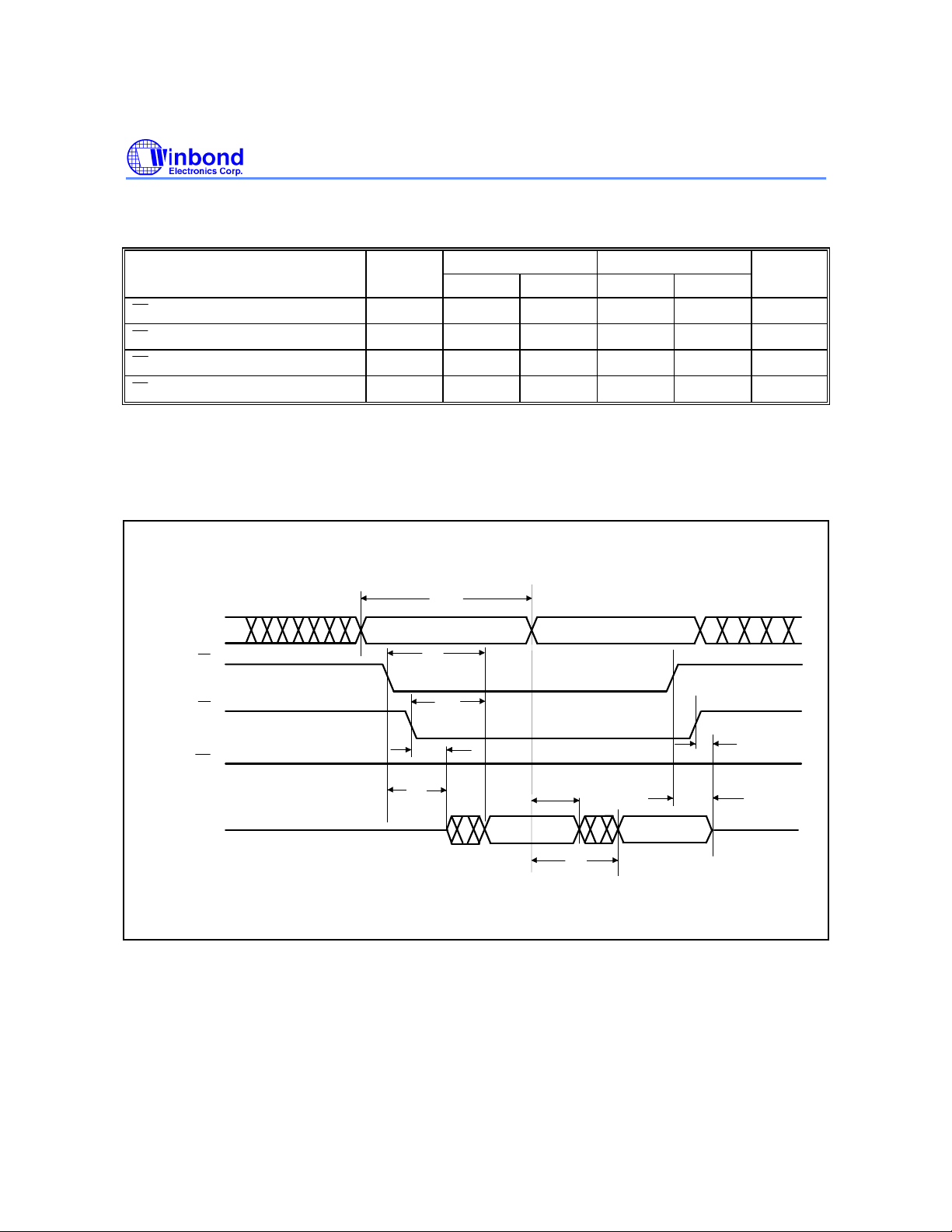
Data Polling and Toggle Bit Timing Parameters
PARAMETER SYM. W49F102-40 W49F102-45 UNIT
to Data Polling Output Delay
to Data Polling Output Delay
to Toggle Bit Output Delay
to Toggle Bit Output Delay
TOEP
TCEP
TOET
TCET
MIN. MAX. MIN. MAX.
- 20 25 nS
- 40 - 45 nS
- 20 - 25 nS
- 40 - 45 nS
TIMING WAVEFORMS
Read Cycle Timing Diagram
W49F102
CE
OE
WE
DQ15-0
High-Z
T
RC
T
CE
T
OE
T
V
IH
TOLZ
T
CLZ
T
Data Valid
OH
T
CHZ
Data Valid
AA
T
OHZ
High-Z
- 14 -
Page 15
Timing Waveforms, continued
WE
CE
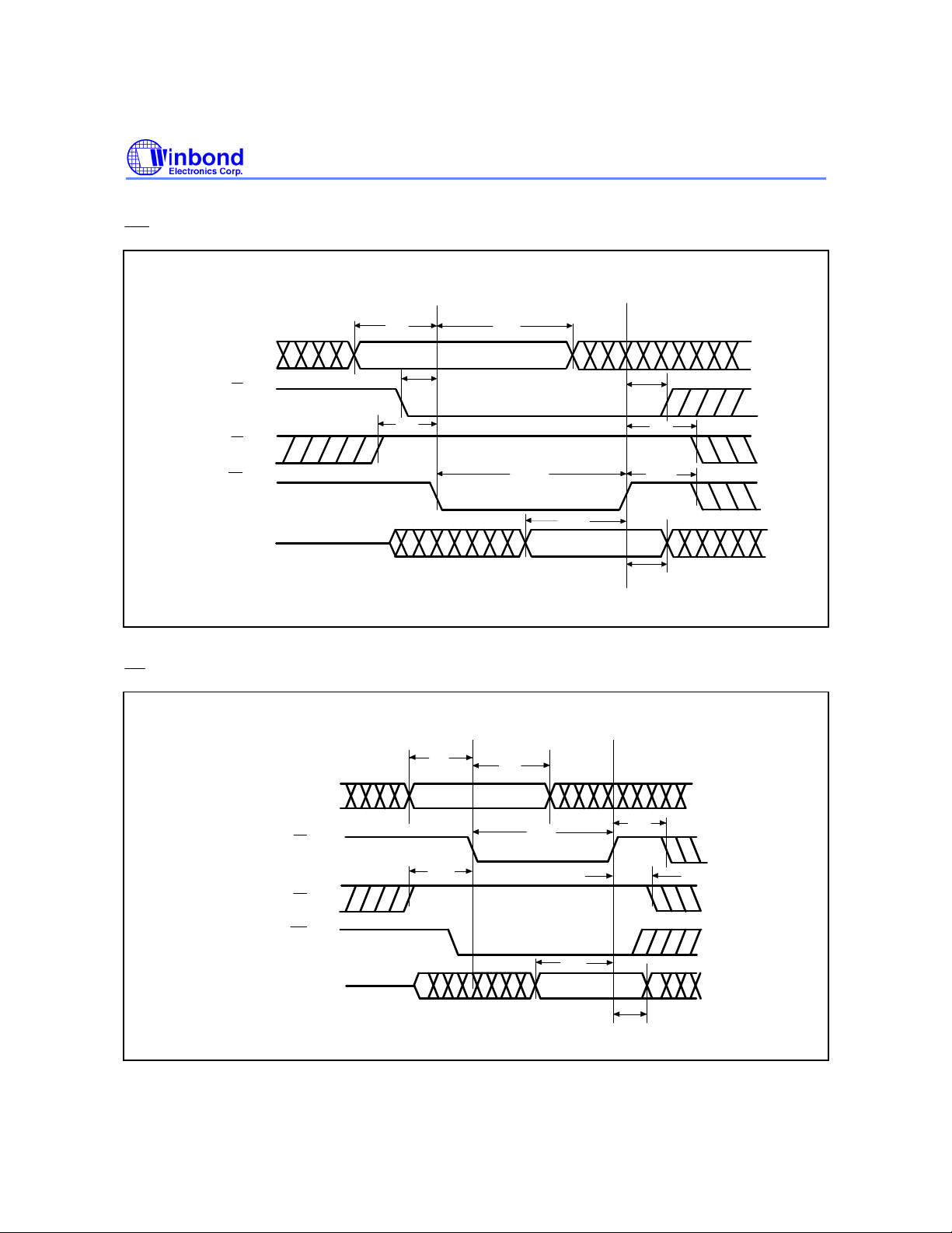
Controlled Command Write Cycle Timing Diagram
W49F102
Address A15-0
CE
OE
WE
DQ15-0
T
AS
T
CS
T
OES
T
AH
T
WP
T
Data Valid
Controlled Command Write Cycle Timing Diagram
AS
T
TAH
T
CH
T
OEH
T
WPH
DS
T
DH
Address A15-0
T
T
T
OEH
DH
CPH
CE
OE
WE
DQ15-0
High Z
T
CP
T
OES
T
DS
Data Valid
Publication Release Date: October 2000
- 15 - Revision A3
Page 16
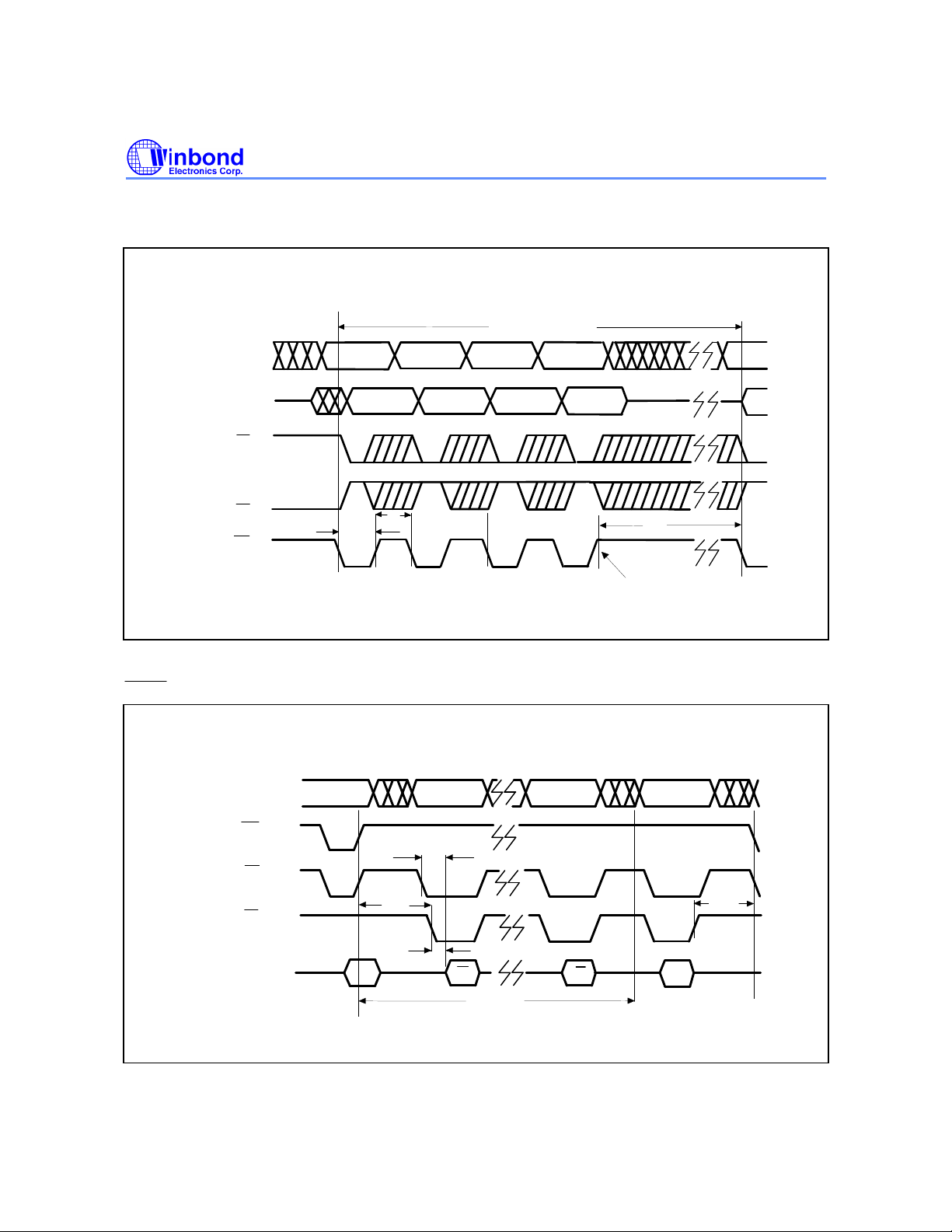
Timing Waveforms, continued
DATA
Program Cycle Timing Diagram
W49F102
Word Program Cycle
Address A15-0
DQ15-0
CE
OE
WE
5555
WP
T
Word 0
AA
Polling Timing Diagram
Address A15-0
T
WPH
Word 1
55552AAA
Word 2
Address
A055
Data-In
Word 3
BP
T
Internal Write Start
WE
T
CEP
CE
T
OEH
OE
T
OEP
DQ7/DQ15
X
X
T
BP or
- 16 -
T
OES
X
T
EC
X
Page 17
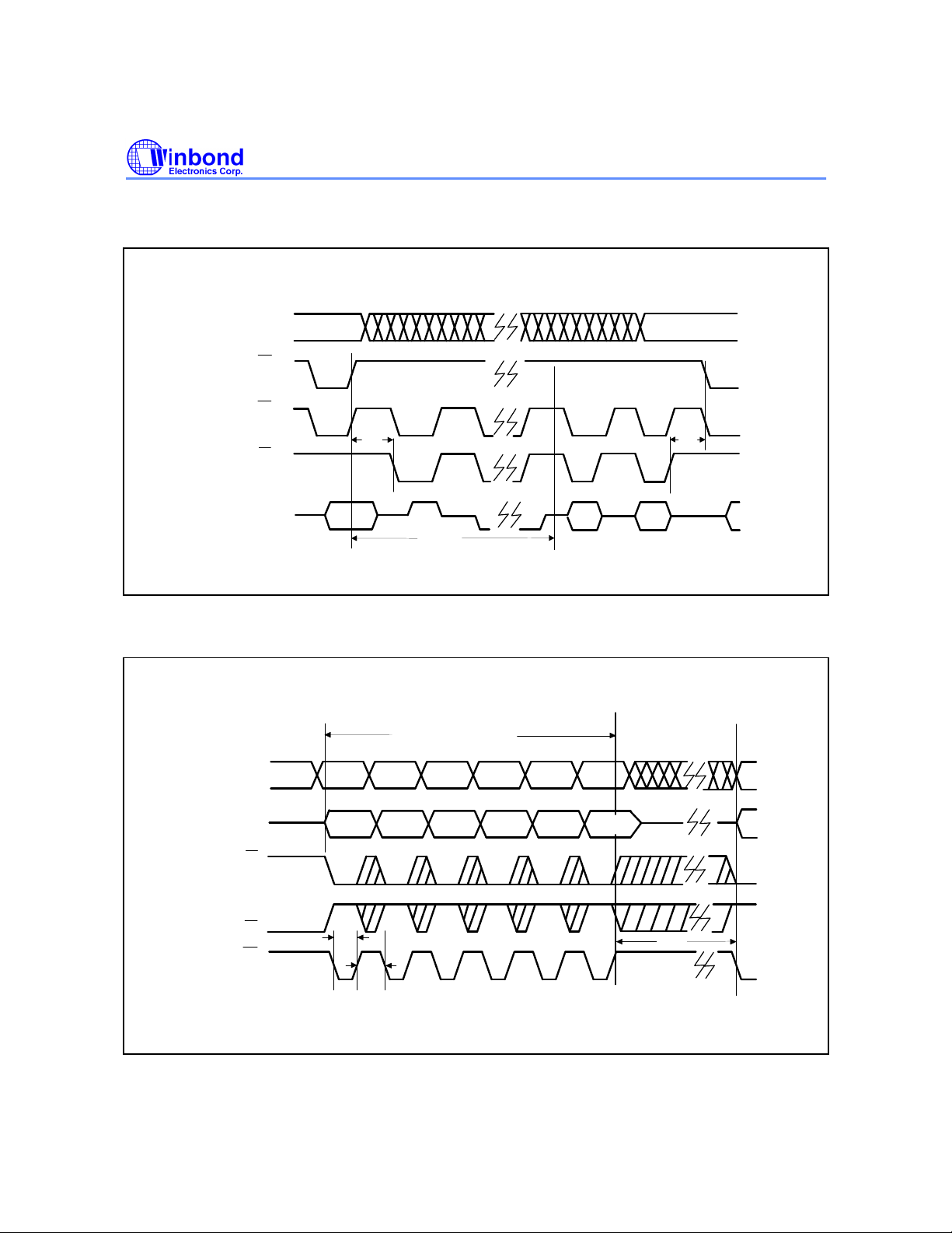
Timing Waveforms, continued
Six-word code for Boot Block
Toggle Bit Timing Diagram
Address A15-0
WE
CE
OE
DQ6/DQ14
TOEH
T
BP orTEC
W49F102
T
OES
Boot Block Lockout Enable Timing Diagram
Lockout Feature Enable
Address A15-0
DQ15-0
CE
OE
WE
5555
XXAA
WP
T
SW0
T
2AAA
WPH
XX55
SW1
5555
XX80
SW23
5555 2AAA
XXAA
SW3
XX55
SW4
5555
XX40
SW5
WC
T
- 17 - Revision A3
Publication Release Date: October 2000
Page 18
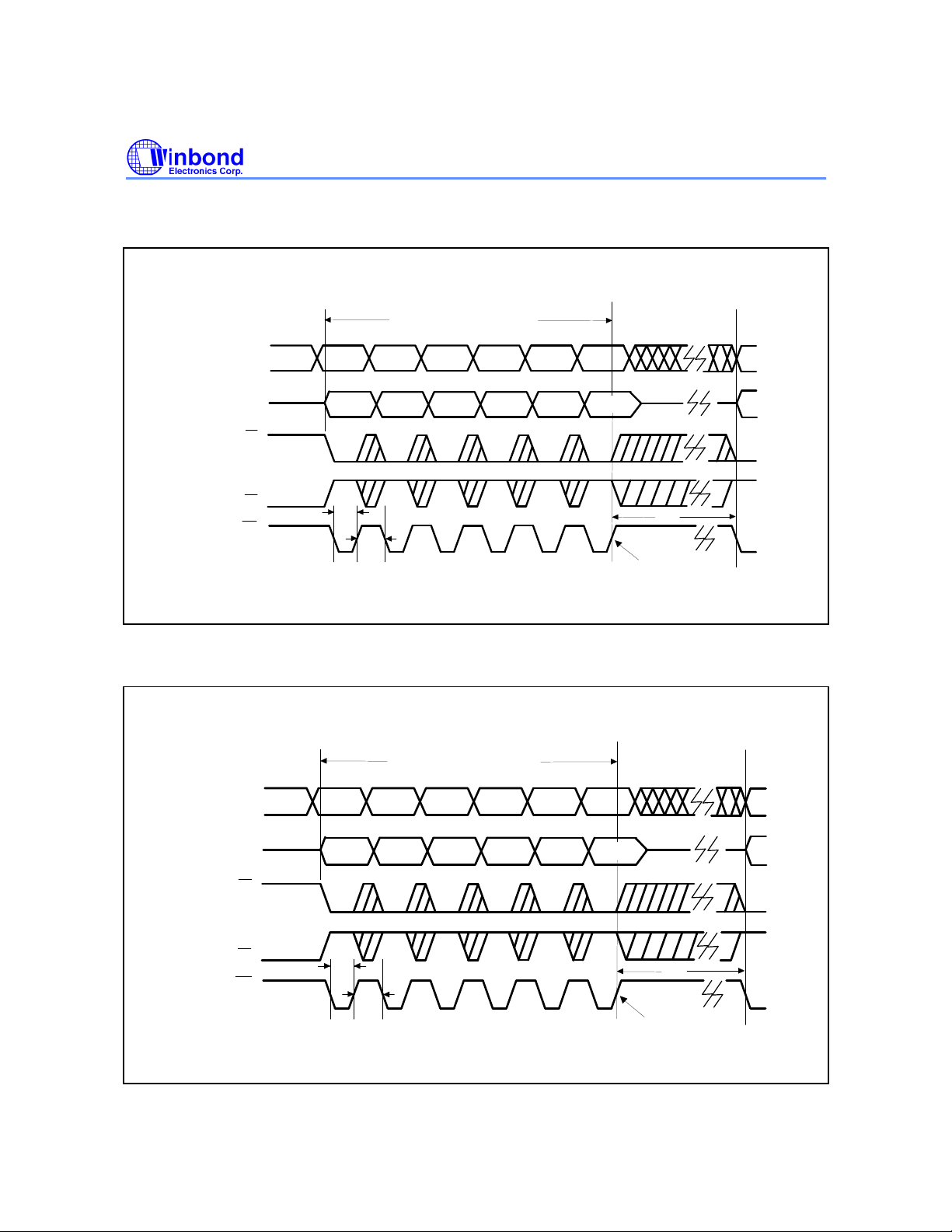
Timing Waveforms, continued
Six-word code for 5V-only software
Chip Erase Timing Diagram
W49F102
Six-word code for 5V-only software
chip erase
Address A15-0
DQ15-0
CE
OE
WE
5555
XXAA
T
WP
SW0
T
2AAA
XX55
WPH
SW1
Main Memory Erase Timing Diagram
Main Memory Erase
Address A15-0
5555
2AAA
5555
XX80
SW2
5555
5555 2AAA
XXAA
SW3
5555 2AAA
XX55
SW4
5555
SW5
5555
XX10
Internal Erase starts
T
EC
- 18 -
DQ15-0
CE
OE
WE
XXAA
T
WP
SW0
T
WPH
XX55
SW1
XX80
SW2
XXAA
SW3
XX55
SW4
XX30
Internal Erase starts
SW5
T
EC
Page 19
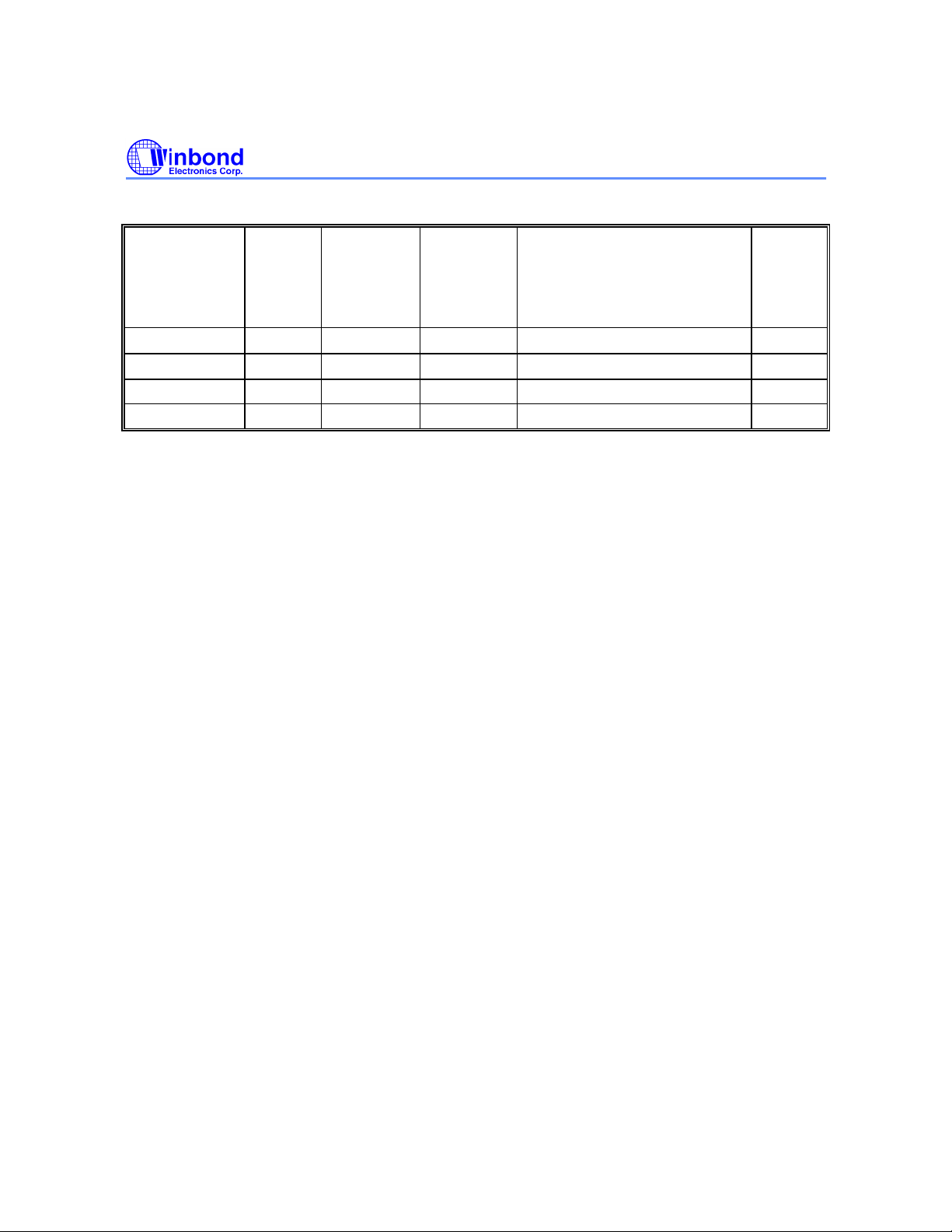
ORDERING INFORMATION
S)
W49F102
Notes:
1. Winbond reserves the right to make changes to its products without prior notice.
2. Purchasers are responsible for performing appropriate quality assurance testing on products intended for use in
applications where personal injury might occur as a consequence of product failure.
PART NO. ACCESS
TIME
(n
W49F102Q40 40 50 100 (CMOS)
W49F102Q45 45 50 100 (CMOS)
W49F102P40 40 50 100 (CMOS) 44-pin PLCC 10K
W49F102P45 45 50 100 (CMOS) 44-pin PLCC 10K
POWER
SUPPLY
CURRENT
MAX.
(mA)
STANDBY
VDD
CURRENT
MAX.
(µA)
PACKAGE CYCLE
40-pin TSOP (10 mm × 14 mm)
40-pin TSOP (10 mm × 14 mm)
10K
10K
Publication Release Date: October 2000
- 19 - Revision A3
Page 20
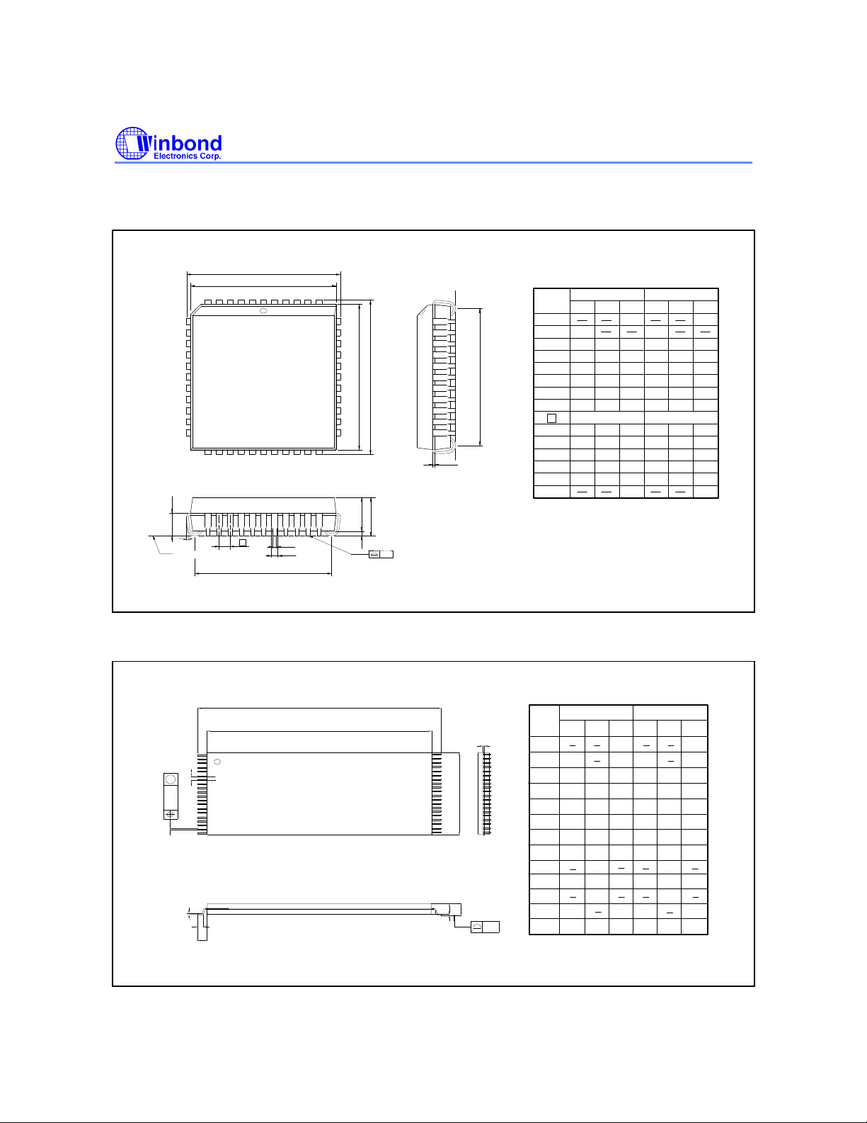
PACKAGE DIMENSIONS
44-pin PLCC
D
H
D
e
44 40
b
b
1
DG
6 1
7
17
L
θ
Seating Plane
W49F102
Dimension in Inches Dimension in mm
Symbol
39
E
E H
29
2818
2
A
A
1
A
y
E
G
c
Min. Nom.
A
0.020
A
1
0.145
2
A
0.026
1
b
0.016
b
0.008
c
0.648
D
0.648
E
e
0.590
D
G
0.590
E
G
0.680
HD
0.680
E
H
0.090
L
y
Notes:
1. Dimension D & E do not include interlead flash.
2. Dimension b1 does not include dambar
protrusion/intrusion.
3. Controlling dimension: Inches
4. General appearance spec. should be based
on final visual inspection spec.
0.050
0.150
0.028
0.018
0.010
0.653
0.653
0.610
0.690
0.690
0.100
BSC
Max.
0.185
0.155
0.032
0.022
0.014
0.658
0.658
0.630
0.6300.610
0.700
0.700
0.110
0.004
0.51
3.68
0.66
0.41
0.20
16.46
16.46
14.99
17.27
17.27
2.29
1.27
Nom.Min.
3.81
0.71
0.46
0.25
16.59
16.59
15.49
15.4914.99
17.53
2.54
BSC
Max.
4.70
3.94
0.81
0.56
0.36
16.71
16.71
16.00
16.00
17.78
17.7817.53
2.79
0.10
40-pin TSOP (10 mm × 14 mm)
D
H
D
e
1
M
0.10(0.004)
b
2
θ
L
L
1
- 20 -
A
A
1
Dimension in Inches
Symbol
c
E
Min. Nom. Max.
A
1
0.002
A
0.037
2
A
b 0.17 0.22 0.270.007
0.039
0.009
c
0.484 0.488 0.492
D
0.390 0.394 0.398
E
D
0.543 0.551 0.559
H
e
L
A
L
Y
Y
θ
Controlling dimension: Millimeters
0.020
1
0.000
0.020
0.024
0.031
0 3 5
Min. Nom. Max.
0.047
0.006
0.011
12.30
13.80
0.028
0.004
Dimension in mm
0.05
0.95
1.00
0.10 0.15 0.200.004 0.006 0.008
12.40
9.90
10
14.00
0.50
0.50
0.60
0.8
0.00
0
3
1.20
0.15
1.050.041
12.50
10.10
14.20
0.70
0.10
5
Page 21
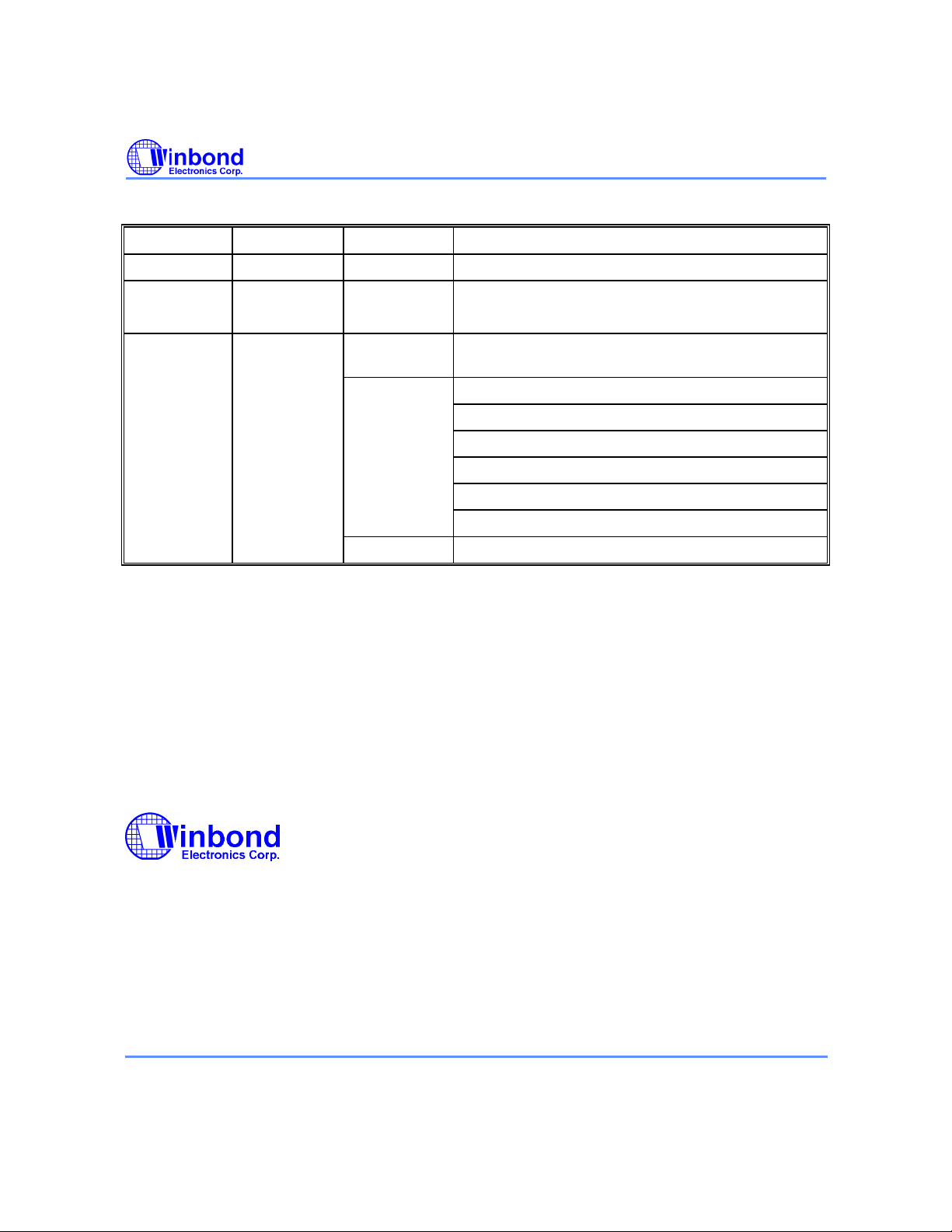
VERSION HISTORY
VERSION DATE PAGE DESCRIPTION
A1 Jun. 1999 - Initial Issued
A2 Oct. 1999 13 Change Read Cycle Timing Parameter:
VDD = 5.0V ±10% for 40, 45, 50, 55, 70 nS
W49F102
A3 Oct. 2000 1, 11, 13, 14,
13 TRC: 35 nS -> 40 nS; 40 nS -> 42 nS
TAH: 50 nS -> 45 nS
TWP & TWPH: 90 nS -> 45 nS
TCP: 90 nS -> 50 nS
Add in TCPH = 50 nS
TDS: 50 nS -> 45 nS
1, 21 Delete 1K cycling option
Delete 35, 50, 55, 70 nS bins
19
Winbond Electronics (H.K.) Ltd.
Headquarters
Headquarters
No. 4, Creation Rd. III,
No. 4, Creation Rd. III,
Science-Based Industrial Park,
Science-Based Industrial Park,
Hsinchu, Taiwan
Hsinchu, Taiwan
TEL: 886-3-5770066
TEL: 886-3-5770066
FAX: 886-3-5792766
FAX: 886-3-5792766
http://www.winbond.com.tw/
http://www.winbond.com.tw/
Voice & Fax-on-demand: 886-2-27197006
Voice & Fax-on-demand: 886-2-27197006
Taipei Office
Taipei Office
11F, No. 115, Sec. 3, Min-Sheng East Rd.,
11F, No. 115, Sec. 3, Min-Sheng East Rd.,
Taipei, Taiwan
Taipei, Taiwan
TEL: 886-2-27190505
TEL: 886-2-27190505
FAX: 886-2-27197502
FAX: 886-2-27197502
Note: All data and specifications are subject to change withou t notice.
Note: All data and specifications are subject to change withou t notice.
Winbond Electronics (H.K.) Ltd.
Unit 9-15, 22F, Millennium City,
Unit 9-15, 22F, Millennium City,
No. 378 Kwun Tong Rd;
No. 378 Kwun Tong Rd;
Kowloon, Hong Kong
Kowloon, Hong Kong
TEL: 852-27513100
TEL: 852-27513100
FAX: 852-27552064
FAX: 852-27552064
Winbond Electronics North America Corp.
Winbond Electronics North America Corp.
Winbond Memory Lab.
Winbond Memory Lab.
Winbond Microelectronics Corp.
Winbond Microelectronics Corp.
Winbond Systems Lab.
Winbond Systems Lab.
2727 N. First Street, San Jose,
2727 N. First Street, San Jose,
CA 95134, U.S.A.
CA 95134, U.S.A.
TEL: 408-9436666
TEL: 408-9436666
FAX: 408-5441798
FAX: 408-5441798
Publication Release Date: October 2000
- 21 - Revision A3
 Loading...