

Page 1
PRELIMINARY
Spread Spectrum 3 DIMM Desktop Clock
W48S87-04
Cypress Semiconductor Corporation
• 3901 North First Street • San Jose • CA 95134 • 408-943-2600
October 19, 1999, rev. **
Features
• Outputs
—4 CPU Clock (2.5V or 3.3V, 50 to 83.3 MHz)
—7 PCI (3.3V)
—1 48- MHz for USB (3.3V)
—1 24-MHz for Super I/O (3.3V)
—2 REF (3.3V)
—1 IOAPIC (2.5V or 3.3V)
—12 SDRAM
• Serial data interface provides additional frequency
selection, individual clock output disable, and other
functions
• Smooth transition supports dynamic frequency
assignment
• Frequency selection not affected during power
down/up cycle
• Supports a variety of power-saving options
• 3.3V operation
• Av ail able in 48-pin SSOP (300 mils)
Key Specifications
±0.5% Spread Spectrum Modulation: .........................±0.5%
Jitter (C y c le -to-Cyc l e ):... ... ...................... .. ... .............. ..2 5 0 ps
Duty Cyc l e: ...... .................................... ... .. ................. 45-55 %
CPU-P C I S kew:.... .................................... ... .. ...........1 to 4 ns
PCI-PC I or CPU-CP U S kew: . .. ....... ... .. ...................... ..2 5 0 ps
Notes:
1. Additional frequency selections provided by serial data interface; refer to
Table 5
on page 10.
2. Signal names in parenthesis denotes function is selectable through mode pin register strapping.
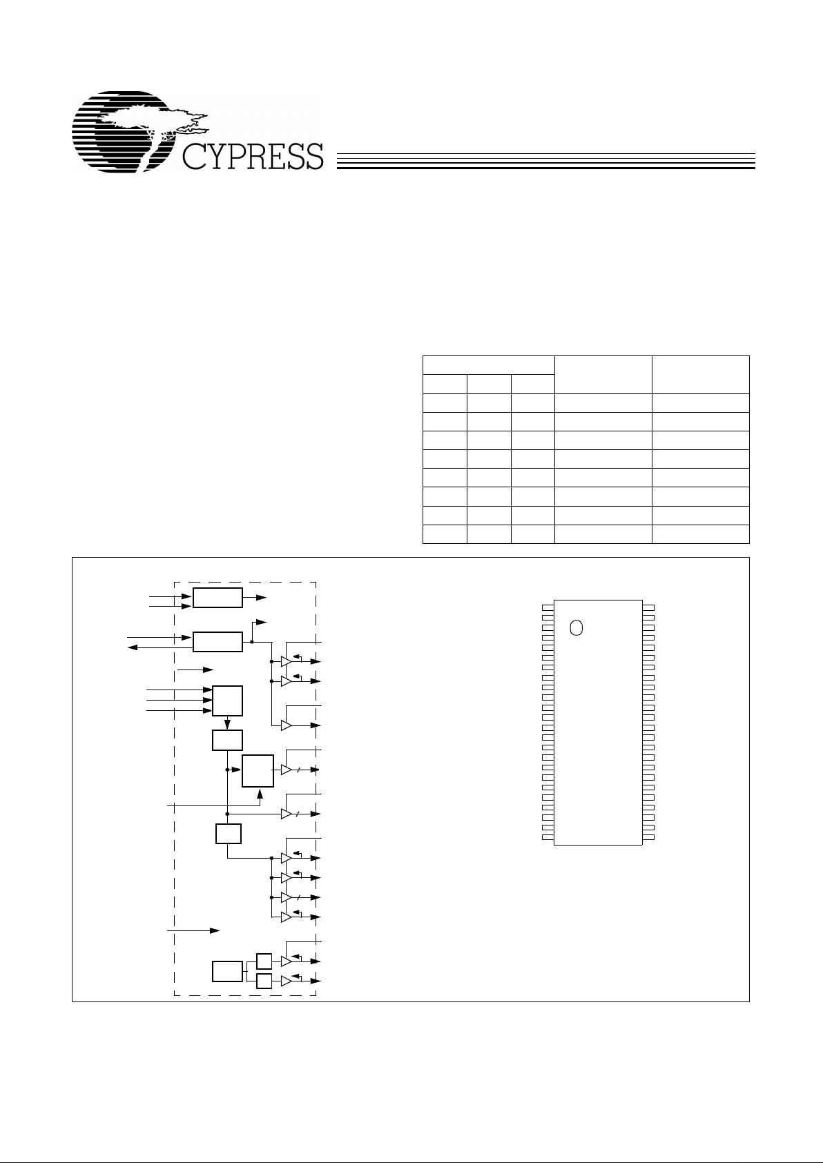
T able 1. Pin Selectable Frequency
[1]
Input Address
CPU, SDRAM
Clocks (MHz)
PCI Clocks
(MHz)FS2 FS1 FS0
0 0 0 50.0 25.0
0 0 1 75.0 32.0
0 1 0 83.3 41.65
0 1 1 68.5 34.25
1 0 0 55.0 27.5
1 0 1 75.0 37.5
1 1 0 60.0 30.0
1 1 1 66.8 33.4
Block Diagram
Pin Configuration
[2]
VDD1
IOAPIC
VDD3
SDRAM0:11
PCI_F/FS1
PCI0/FS2
XTAL OSC
PLL Ref
PLL1
X2
X1
REF1(CPU_ST OP#)
Stop
Clock
Cntrl
PCI1:4
PWR_DWN#
Power Down
Control
PCI5(PWR_DWN#)
48MHZ/FS0
24MHZ/MODE
PLL2
Serial Port
SCLOCK
SDA TA
Device
CPU_STOP#
Control
CPU3.3#_2.5
CPU Clock
Mode Control
÷4
÷2
I/O
I/O
VDD1
MODE
4
I/O
I/O
VDD2
12
CPU0:3
4
VDDL2
÷2
VDDL1
MODE
I/O
REF0/CPU3.3#_2.5
Freq
Select
FS0
FS1
FS2
Freq
VDD1
REF0/CPU3.3#_2.5
GND
X1
X2
VDD2
PCI_F/FS1
PCI0/FS2
GND
PCI1
PCI2
PCI3
PCI4
VDD2
PCI5(PWR_DWN#)
GND
SDRAM11
SDRAM10
VDD3
SDRAM9
SDRAM8
GND
SDATA
SCLOCK
W48S87-04
VDDL1
IOAPIC
REF1(CPU_STOP#)
GND
CPU0
CPU1
VDDL2
CPU2
CPU3
GND
SDRAM0
SDRAM1
VDD3
SDRAM2
SDRAM3
GND
SDRAM4
SDRAM5
VDD3
SDRAM6
SDRAM7
GND
48MHZ/FS0
24MHZ/MODE
48
47
46
45
44
43
42
41
40
39
38
37
36
35
34
33
32
31
30
29
28
27
26
25
1
2
3
4
5
6
7
8
9
10
11
12
13
14
15
16
17
18
19
20
21
22
23
24
Page 2
W48S87-04
PRELIMINARY
2
Pin Definitions
Pin Name
Pin
No.
Pin
Type Pin Description
CPU0:3 44, 43, 41, 40O
CPU Clock Outputs 0 through 3:
These four CPU clock output s are controll ed
by the CPU_STOP# control pi n. Output voltage swing is controlled by voltage
applied to VDDL2 and output characteristics are adj usted by input
CPU3.3#_2.5.
PCI_F/FS1 7 I/O
Fixed PCI Cloc k Output and Frequency Selection Bit 1:
As an output, this
pin works in conjunction with PCI0:5. Output vol tage swing is control led by
voltage applied to VDD2.
When an input, this pin functions as part of the frequency selection address.
The value of FS0:2 determines the po wer-up def ault freque ncy of devi ce output
clocks as per the Table 1, “Pin Selectable Frequency” on page 1.
PCI0/FS2 8 I/O
PCI Bus Clock Output 0 and Frequency Selection Bit 2:
As an output, this
pin works in conjunction with PCI1:5 and PCI_F. Output voltage swing is controlled by voltage applied to VDD2.
When an input, this pin functions as part of the frequency selection address.
The value of FS0:2 determines the po wer-up def ault freque ncy of devi ce output
clocks as per the Table 1, “Pin Selectable Frequency” on page 1.
PCI1:4 10, 11, 12, 13O
PCI Bus Clock Outputs 1 through 4:
Output volt age swing is controlled by
voltage applied to VDD2.
PCI5(PWR_DWN#) 15 I/O
PCI Bus Cloc k Output 5 o r Power- Down Control:
As an output, this pin works
in conjunction wi th PCI0:4 and PCI_F. Output voltage s wing is controlled by
voltage applied to VDD2.
If progr ammed as an input ( ref er to MO DE pin descript ion), this pi n is used f or
power-down control. When LOW, the device goes into a low-power standby
condition. All outputs are activel y held LOW while in power-down. CPU,
SDRAM, and PCI clock out puts ar e stopped LO W after com pleting a f ull cl ock
cycle (2–4 CPU cloc k cycle late ncy). When b rought HIGH, CPU , SDRAM, an d
PCI outputs start with a full clock cycle at full operating frequency (3 ms maximum latency).
SDRAM0:11 38, 37, 35,
34, 32, 31,
29, 28, 21,
20, 18, 17
O
SDRAM Clock Outputs 0 through 11:
These twelve SDRAM clock outputs
run synchronous to the CPU clo ck outputs. Output vol tage swing is controlled
by volt age applied to VDD3.
IOAPIC 47 O
I/O APIC Clock Output:
Provides 14.31 8-MHz fixed frequency. The output
voltage swing is controlled by VDDL1.
48MHZ/FS0 26 I/O
48-MHz Output and Frequency Selection Bit 0:
Fixed clock output that default s to 48 MHz f oll o wing de vice po w er-up . Output voltage swing is controll ed
by volt age applied to VDD1.
When an input, this pin functions as part of the frequency selection address.
The value of FS0:2 determines the po wer-up def ault freque ncy of devi ce output
clocks as per the Table 1, “Pin Selectable Frequency” on page 1.
24MHZ/MODE 25 I/O
24-MHz Output and Mode Contr ol Input:
Fixed cloc k output that defaults to
24 MHz following device power-up. Output voltage swing is controlled by voltage applied to VDD1.
When an input, this pin i s used for pin programming selection . It determines
the functio ns for pins 15 and 46:
MODE Pin 15 Pin 46
0 PWR_DWN# (input) CPU_STOP# (input)
1 PCI5 (output) REF1 (output)
Page 3
W48S87-04
PRELIMINARY
3
REF0/CPU3.3#_2.5 2 I/O
Fixed 14.318-MHz Output 0 and CPU Output Voltage Swing Selection
Input:
As an output, this pin is used for various sy stem applications. Output
voltage swing is controlled b y v olt age appli ed to VDD1. REF0 is stro nger than
REF1 and should be used for driving ISA slots.
When an input, thi s pin selects the CPU clock output buff er charac teristics th at
are optimiz ed for either 3.3V or 2.5V ope ration.
CPU3.3#_2.5 VDDQ2 Voltage (CPU0:3 Swing)
03.3V
12.5V
This input a djusts CPU clock output impedance so that a nominal 20Ω output
impedance is maintained. This eliminates or reduces the need to adjust ext ernal clock t uning components when changing VDDL2 v oltage. CPU cloc k phase
is also adjusted so that both CPU and SDRAM and CPU-to-PCI clock ske w is
maintained over the two VDDL2 voltage options. This input does not adjust
IOAPIC cl ock output charact e ri stics.
REF1(CPU_Stop#) 46 I/O
Fixed 14.318-MHz Output 0 or CPU Clock Output Stop Control:
Used for
various syst em applications. O utput voltage sw ing is controlled by voltage applied to VDD1. REF0 i s stronger than REF 1 and shoul d be used f or driving ISA
slots.
If progr ammed as an input ( ref er to MO DE pin descript ion), this pi n is used f or
stopping the CPU clock outputs. When brought LOW, clock outputs CPU0:3
are stopped LOW after completing a full clock cycle (2–3 CPU clock l atency).
When brought HI GH, clock outputs CPU0:3 are starting beginning with a full
clock cy c l e (2–3 CPU clock latency).
X1 4 I
Crystal Connection or External Reference Frequency Input:
This pin has
dual functions. It can be used as an external 14.318-MHz crystal connect ion
or as an external reference frequency input.
X2 5 I
Crystal Connection :
An input conn ection f or an ex ternal 14. 318-MHz crystal.
If using an external r eference, this pin must be left unconnected.
SDATA 23 I
Serial Data Input:
Data input for Serial Dat a In terface. Re fer to Serial Data
Interface section that follows.
SCLOCK 24 I
Serial Clock Input:
Clock input for Serial Data Interface. Refer to Serial Data
Interface section that follows.
VDD1 1 P
Powe r Connect ion:
Power supply for crystal oscillator and REF0 :1 output
buffers. Connected to 3.3V suppl y.
VDD2 6,14 P
Powe r Connection:
Po wer supply for PCI clock output buffers. Connected to
3.3V supply.
VDDL1 48 P
Powe r Connection:
Po wer supply f or IOAPIC out put buffer . Connected to 2.5V
or 3.3V supply.
VDDL2 42 P
Powe r Connect ion:
Po wer supply for CPU clock output b u ff ers. Connect ed to
2.5V or 3.3V supply.
VDD3 19, 30, 36 P
Powe r Connection:
Pow er supply f or SDRAM clock o utput buff ers. Conn ected
to 3.3V supply.
GND 3, 9, 16, 22,
27, 33, 39,
45
G
Ground Connection:
Connect all ground pin s to the comm on system gr ound
plane.
Pin Definitions
(continued)
Pin Name
Pin
No.
Pin
Type Pin Description
Page 4
W48S87-04
PRELIMINARY
4
Overview
The W48S87-04, a motherboard clock synthesizer, can provide eith er a 2.5V or 3.3 V CPU clock swing, making i t suitabl e
for a variety of CPU options. Twelve SDRAM clocks are provided in phase wit h the CPU cloc k outputs . This pro vides clock
support for up to three SDRAM DlMMs. Fixed outp ut frequency
clocks are pr ovided for oth er system functions.
Functional Description
I/O Pin Operation
Pins 2, 7, 8, 25, and 26 ar e dual-purpose l/O pins . Upon powerup these pins act as log ic in puts, all owing the det erminatio n of
assigned device functions. A short time after power-up, the
logic state of these pins is latched and the pins then become
clock outputs. This feature reduces device pin count by combining cloc k outputs with input selec t pi ns.
An external 10-kΩ “strapping” resistor is connected between
each l/O pin and ground or V
DD3
. Connection to gr ound s ets a
latch to “0”, connection to V
DD3
sets a latch to “1”. Figure 1 an d
Figure 2 show two suggested methods for strapping resistor
connection.
Upon W48S87-04 pow er-up , the first 2 ms of op eration is use d
for inpu t logic selecti on. During this period, these dual-purpose
I/O pins are three-state d, allo wing the ou tput str apping re sistor
on each l/O pin to pull the pin and its associated capacitive
clock load to either a logic HIGH or LOW state. At the end of
the 2-ms period, the establi shed logic 0 or 1 condition of each
l/O is pin is then latched. Next the output buffers are enabled ,
which converts the l/O pins into operating clock outputs. The
2-ms timer is started when V
DD
reaches 2.0V. The input bits
can only be reset by turning V
DD
off and then back on again.
It should be noted that the strapping resistors have no significant effect on clock output signal integrity. The drive impedance of both cloc k output s is <40Ω (nominal) whic h is minimal ly affected by the 10-kΩ strap to ground or V
DD
. As with the
series termination resist or, the output strapping res istor should
be placed as close to the l/O pin as possible in order to keep
the interconnecting trace short. The trace from the resistor to
ground or VDD should be kept less than two inches in length
to prevent system noise coupling duri ng input logic sampling.
When the clock out puts are enabled following the 2-ms input
period, target ( normal) output f requenc y is deliv ered a ssuming
that V
DD
has stabilized. If VDD has not yet reached full value,
output frequency in iti ally ma y be below t arget b ut wil l in crease
to target once V
DD
voltage has stabilized. In either case, a
short output clock cycle may be produced from the CPU clock
outputs when the outputs are enabled.
Power-on
Reset
Timer
Output Three-state
Data
Latch
Hold
QD
W48S87-04
V
DD
Clock Load
22
Ω
10 k
Ω
Output
Buffer
(Load O ption 1)
10 k
Ω
(Load O ption 0)
Output
Low
Output Strapping Resistor
Series Termination Resistor
Figure 1. Input Logic Selection Thr ough Resistor Load Option
Power-on
Reset
Timer
Output Three-state
Data
Latch
Hold
QD
W48S87-04
V
DD
Clock Load
R
10 k
Ω
Output
Buffer
Output
Low
Output Strapping Resistor
Series Termination Resistor
Jumper Options
Figure 2. Input Logic Selection Thr ough Jumper Option
Resistor Value R
39
Ω
33
Ω
Output
IOAPIC, SDRAM
All other clock outputs
Page 5

W48S87-04
PRELIMINARY
5
CPU/PCI Freq uency Selection
CPU frequency is selected with I/O pins 26, 7, and 8
(48MHz/FS0, PCI_F/FS1, and PCI0/FS2, respectively). Refer
to Table 1 for CPU/PCI frequency programming infor mation.
Additional fr equency sel ect ions ar e av ailab l e throug h the serial data interf ace. Refer to Table 5 on page 10.
Output Buffer Configuration
Clock Output s
All clock outputs are designed to drive serial terminated clock
lines. T he W48S87-04 out put s are CMOS -type , whic h prov ide
rail-to-rail output swing. To accommodate the limited voltage
swing required by some processors, the output buffers of
CPU0:3 use a special VDDL2 power supply pin that can be
tied to 2.5V nominal.
Crystal Oscillator
The W48S87-04 requires one input ref erence clock to synthesize all output frequencies. The reference clock can be either
an externall y gener ated clo c k signal or the cl ock gen er ated by
the internal crystal oscillator. When using an ex ternal clock
signal, pin X1 is us ed as the cloc k input and pi n X2 is left open .
The input threshold voltage of pin X1 is V
DD
/2.
The internal crystal oscillator is used in conjunction with a
quartz crystal connected t o de vi ce pins X 1 and X2 . Th is f orms
a parallel resonant crystal oscillator circuit. The W48S87-04
incorporates the necessary f ee dback r esist or and crystal load
capacitors . Inclu ding typi cal st ra y ci rcuit capac itanc e, the total
load presented to the crystal is approximately 20 pF. For optimum frequency accuracy without the addition of external capacitors, a parallel-resonant mode crystal specifying a load of
20 pF should be used. This will typically yield reference frequency accuracies within ±100 ppm.
Dual Supply Voltage Operation
The W48S87-04 is designed for dual power supply operation.
Supply pins VDD1, VDD2, and VDD3 a re co nnected t o a 3.3V
supply and supply power to th e internal core circuit and to the
clock output buffers, except for outputs CPU0:3 and IOAPIC.
Supply pins VDDL1 and VDDL2 ma y be connected to either a
2.5V or 3.3V supply.
Page 6
W48S87-04
PRELIMINARY
6
Spread Sp ectrum Generator
The device generates a clock that is frequency modulated in
order to increase the bandwidth that it occu pies. By increas ing
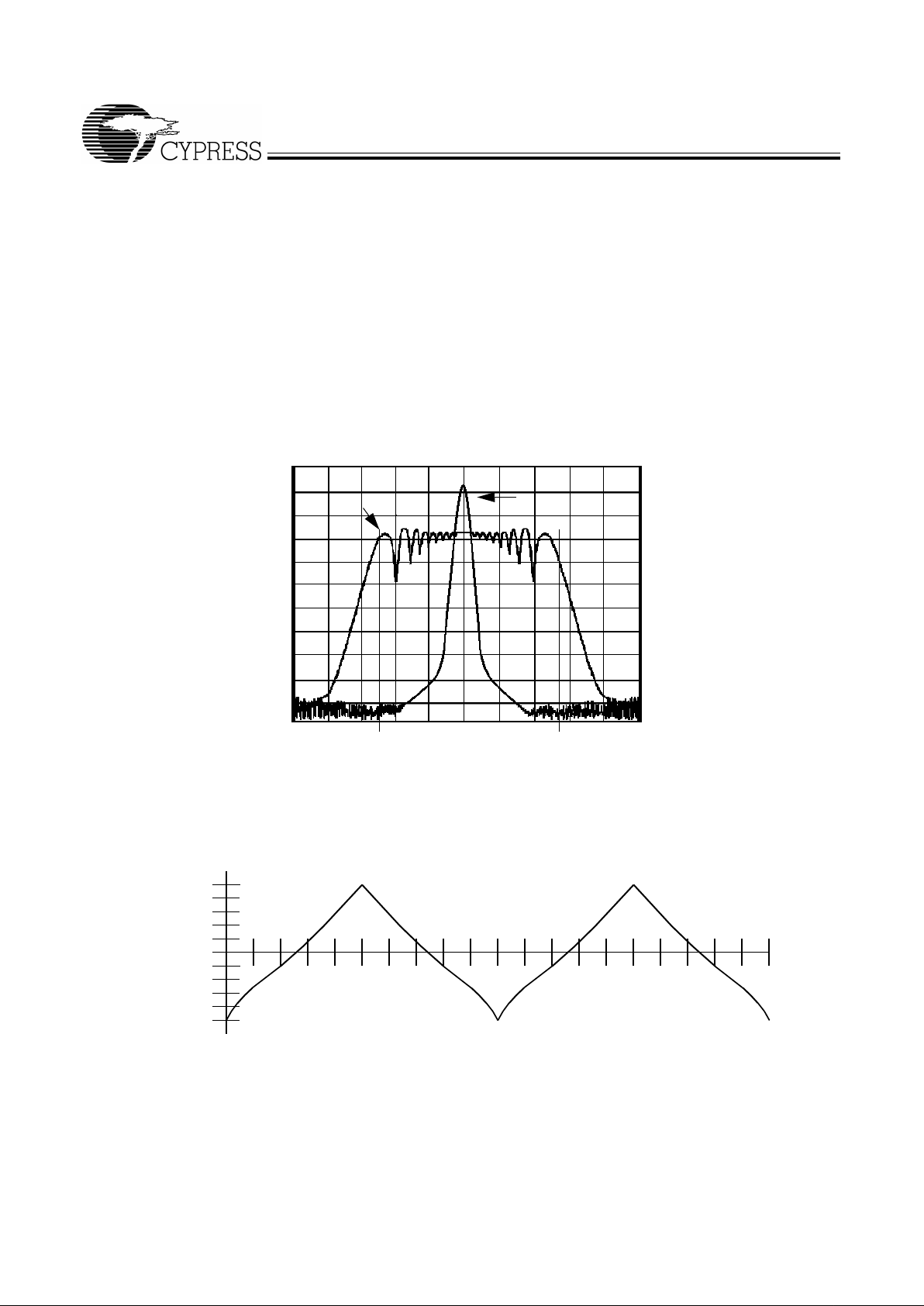
the bandwidth of the fundamental and its harmonics, the amplitudes of the radiated electromagnetic emissions are reduced. This effect is depicted in Figure 3.
As depicted in Figure 3, a harmonic of a modulated clock has
a much lower amplitude than that of an unmodulated signal.
The reduction in am plitude is dependen t on the harmonic number and the frequency deviation or spread. The equation for
the reductio n is
dB = 6.5 + 9*log
10
(P) + 9*log10(F)
Where P is the per cent age of de viat i on and F is the freq uency
in MHz where the reduction is measured.
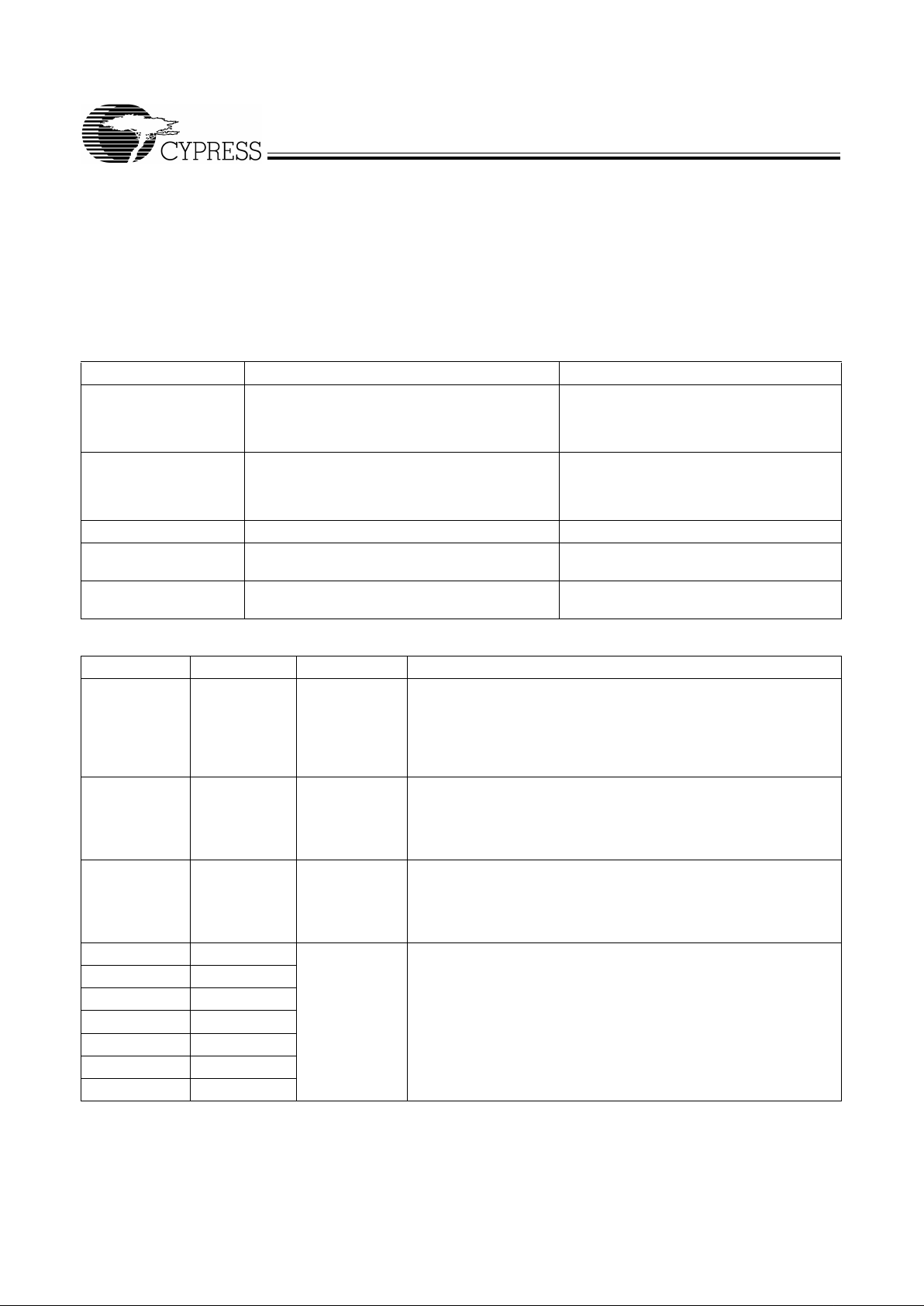
The output clock is modulated with a waveform depicted in
Figure 4. This waveform, as discussed in “Spread Spect rum
Clock Generation f or the Reducti on of Radiated Emissio ns” by
Bush, Fessler, and Hardin produces the maximum reduction
in the amplitude of radiated electromagnetic emissions. The
deviati on select ed fo r th is chip is ±0. 5% of the ce nter frequen cy. Figure 4 details the Cypress spreading pattern. Cypress
does offer options with more spread and greater EMI reduction. Contact your local Sales representative for details on
these devices.
Spread Spectrum clocking is activated or deactivated by selecting the appropriate v al ues fo r bits 1–0 in data byte 0 of the
I
2
C data stream. Refer to Table 4 for more detail s.
Figure 3. Clock Harmonic with and without SSCG Modulation Frequency Domain Representation
SSFTG Typical Clock
Frequency Span (MHz)
+1.0
-SS%
+SS%
Amplitude (dB)
5dB/di v
Figure 4. Typica l Modulation Profile
MAX (+.0.5%)
MIN. (–0.5%)
10%
20%
30%
40%
50%
60%
70%
80%
90%
100%
10%
20%
30%
40%
50%
60%
70%
80%
90%
100%
FREQUENCY
Page 7
W48S87-04
PRELIMINARY
7
Serial Data Interface
The W48S87-04 features a two-pin, serial data interface that
can be used to configure internal register settings that control
particular device functions. Upon power-up, the W48S87-04
initiali zes with defaul t registe r setti ngs, t herefo re the use of this
serial data interface is optional. The serial interface is writeonly (to the clock chip) and is the dedicated function of device
pins SDATA and SCLOCK. In motherboard applications,
SDATA and SCLOCK are typically driven by two logic outputs
of the chipset. Clock device register changes are normally
made upon system initialization, i f any are required. The interface can also be us ed during system oper ation f or power management functions. Table 2 summarizes the control functions
of the serial data interface.
Operation
Data is written to the W48S87-04 in ten bytes of eight bits
each. Bytes are written in the or der shown in Table 3.
T able 2. Serial Data Interface Control Func ti ons Sum mary
Control Function Description Common Application
Clock Output Disable Any indivi dual clock output(s) can be disabled. Dis-
abled outputs ar e actively held LO W.
Unused outputs are di sabled to reduce EMI
and system power. Examples are clock outputs to unused SDRAM DIMM socket or PCI
slot.
CPU Clock Frequency
Selection
Provides CPU/PCI fr equency selections be yond the
50- and 66.8-MHz selections that are provided by
the FS0:2 power- on defaul t selection. Frequ ency is
changed in a smooth and controlled fashion.
For alternate CPU devi ces, and power management options. Smooth frequency transition allows CPU fr equency ch ange un der nor-
mal system operati on.
Output Three-state Puts all clock outputs into a high-impedance state. Production PCB testing.
Test Mode All clock outputs toggle in relat ion with X1 input,
internal PLL is bypassed. Refer to Tabl e 4.
Production PCB testing.
(Reserved) Reserved functio n for future de vice revisi on or pro-
duc tion dev ice tes t i ng.
No user application . Regist er bit must be wri t-
ten as 0.
Table 3. Byte Writing Sequence
Byte Sequence Byte Name Bit Sequence Byte Description
1 Slave Address 11010010 Commands the W48S87-04 to accept the bits in Data Byte s 0 –6 f or
internal register configuration. Since other devices may exist on the
same common serial data bus, it is necessary to have a specific slave
address for each potential receiver. The slave receiver address for the
W48S87-04 is 11010010. Regi ster set ting will not be made if the Sla v e
Add r ess is n ot corr ect (or is for an alter nat e slave rec e i ve r).
2 Command
Code
Don’t Care Unused by the W48S87-04, therefore bit values are ignored (“don’t
care”). This b yte must be included in the data write se quence to mai ntain
proper byte all ocation. The Command Code Byt e is part of the standar d
serial communicat ion protocol and may be us ed when writing to another
addressed slave receiver on the serial data bus.
3 Byte Count Don’t Care Unused by the W48S87-04, therefore bit values are ignored (“don’t
care”). This b yte must be included in the data write se quence to mai ntain
proper byte allo cation. The Byte Count Byt e is part of the standard serial
communication protocol and may be used when writin g to anot her addressed slave receiver on the serial data bus.
4 Data Byte 0 Refer to Ta ble 4 The data bits in these bytes set internal W48S87-04 registe rs that con-
trol dev ice oper ation. Th e data bits are only a ccepted when the Addr ess
Byte bit sequence is 11010010, as noted above. For description of bit
control functions, refer to Table 4, Data Byte Serial Configurati on M ap.
5 Data Byte 1
6 Data Byte 2
7 Data Byte 3
8 Data Byte 4
9 Data Byte 5
10 Data Byte 6
Page 8

W48S87-04
PRELIMINARY
8
Writing Data Bytes
Each bit in the data bytes control a particular device function
except for the “reserved” bits which must be written as a logic
0. Bits are written MSB (most significant bit) first, which is bit
7. Ta b le 4 gives the bit form ats for registers located in Data
Bytes 0–6. Table 5 details addi tional fre quency selections that
are available through the serial data interface. Ta ble 6 detai ls
the select functions for Byte 0, bits 1 and 0.
Table 4. Data Bytes 0–6 Seri al Conf iguration Map
Bit(s)
Affected Pin
Control Function
Bit Control
DefaultPin No. Pin Name 0 1
Data Byte 0
7-- --(Reserved) -- -- 0
6 -- -- BYT0_SEL2 Refer to Ta ble 5 0
5 -- -- BYT0_SEL1 Refer to Ta ble 5 0
4 -- -- BYT0_SEL0 Refer to Ta ble 5 0
3 BYT0 _FS# Frequency
Cont rolle d by
FS (2:0)
Frequency
Controlled by
BYT0_SEL (2:0)
0
222 (Reserved) 0
1–0 -- -- Bit 1 Bit 0 Function (See Table 6 for function detail s)
0 0 Normal Operation
01 Test Mode
1 0 Spread Spectrum On
1 1 All Outputs Thr ee-stated
00
Data Byte 1
7 26 48MHZ Clock Output Disable Low Active 1
6 25 24MHZ Clock Output Disable Low Active 1
5-- --(Reserved) -- -- 0
4-- --(Reserved) -- -- 0
3 40 CPU3 Clock Output Disable Low Active 1
2 41 CPU2 Clock Output Disable Low Active 1
1 43 CPU1 Clock Output Disable Low Active 1
0 44 CPU0 Clock Output Disable Low Active 1
Data Byte 2
7-- --(Reserved) -- -- 0
6 7 PCI_F Clock Output Disable Low Active 1
5 15 PCI 5 Clock Output Disable Low Active 1
4 13 PCI 4 Clock Output Disable Low Active 1
3 12 PCI 3 Clock Output Disable Low Active 1
2 11 PCI 2 Clock Output Disable Low Active 1
1 10 PCI 1 Clock Output Disable Low Active 1
0 8 PCI0 Clock Output Disable Low Active 1
Page 9

W48S87-04
PRELIMINARY
9
Data Byte 3
7 28 SDRAM7 Clock Output Disable Low Active 1
6 29 SDRAM6 Clock Output Disable Low Active 1
5 31 SDRAM5 Clock Output Disable Low Active 1
4 32 SDRAM4 Clock Output Disable Low Active 1
3 34 SDRAM3 Clock Output Disable Low Active 1
2 35 SDRAM2 Clock Output Disable Low Active 1
1 37 SDRAM1 Clock Output Disable Low Active 1
0 38 SDRAM0 Clock Output Disable Low Active 1
Data Byte 4
7-- --(Reserved) -- -- 0
6-- --(Reserved) -- -- 0
5-- --(Reserved) -- -- 0
4-- --(Reserved) -- -- 0
3 17 SDRAM11 Clock Output Disable Low Active 1
2 18 SDRAM10 Clock Output Disable Low Active 1
1 20 SDRAM9 Clock Output Disable Low Active 1
0 21 SDRAM8 Clock Output Disable Low Active 1
Data Byte 5
7-- --(Reserved) -- -- 0
5-- --(Reserved) -- -- 0
5-- --(Reserved) -- -- 0
4 47 IOAPIC Clock Output Disable Low Active 1
3-- --(Reserved) -- -- 0
2-- --(Reserved) -- -- 0
1 46 REF1 Clock Output Disable Low Active 1
0 2 REF0 Clock Output Disable Low Active 1
Data Byte 6
7-- --(Reserved) -- -- 0
6-- --(Reserved) -- -- 0
5-- --(Reserved) -- -- 0
4-- --(Reserved) -- -- 0
3-- --(Reserved) -- -- 0
2-- --(Reserved) -- -- 0
1-- --(Reserved) -- -- 0
0-- --(Reserved) -- -- 0
Table 4. Data Bytes 0–6 Seri al Conf iguration Map
(continued)
Bit(s)
Affected Pin
Control Function
Bit Control
DefaultPin No. Pin Name 0 1
Page 10

W48S87-04
PRELIMINARY
10
Note:
3. CPU, SDRAM, and PCI frequency selections are listed in
Table 1
and
Table 5
.
4. In Test Mode, the 48/24MHz clock outputs are:
- X1/2 for 48-MHz output.
- X1/4 for 24-MHz output.
T able 5. Additional Frequency Selections through Serial Data Interface Data Bytes
Input Conditions Output Frequency
Data Byte 0, Bit 3 = 1
CPU, SDRAM Clocks
(MHz)
PCI Clocks
(MHz)
Bit 6
BYT0_SEL2
Bit 5
BYT0_SEL1
Bit 4
BYT0_SEL0
0 0 0 50 25
00175.032
0 1 0 83.3 41.65
0 1 1 68.5 34.25
1 0 0 55.0 27.5
1 0 1 75.0 37.5
1 1 0 60.0 30.0
1 1 1 66.8 33.4
T able 6. Select Function for Data Byte 0, Bits 0:1
Function
Input Conditions Output Conditions
Data Byte 0
CPU0:3,
SRAM0:11
PCI_F,
PCI0: 5 REF0:1 , IOAPI C 48 /2 4 M H ZBit 1 Bit 0
Normal Operation 0 0 Note 3 Note 3 14.318 MHz 48/24 MHz
Test Mode 0 1 X1/2 X1/4 X1 Note 4
Spread Spectrum 1 0 Note 3
SS±0.5%
Note 3
SS±0.5%
14.318 MHz 48/24 MHz
Three-state 1 1 Hi-Z Hi-Z Hi-Z Hi-Z
Page 11

W48S87-04
PRELIMINARY
11
How To Use the Serial Data Interface
Electrical Requirements
Figure 5 illust rat es el ectrical ch aract eristi cs for the serial interface bus used with the W48S87-04. Devices send data over
the bus with an open drain logi c output that can (a) pull the bus
line LOW, or (b) let t he b u s def au lt t o logi c 1. The pu ll- up resi stors on the bus (both clock and data lines) establish a default
logic 1. All bus devices generally have logic inputs to receive
data.
Although the W48S87-04 is a receive-only device (no data
write-back capabi lity), it does transmit an “acknowledge” data
pulse after each by te is received. Thus, the SDATA line can
both transmit and receive data.
The pull-up resistor should be sized to meet the rise and fall
times specif ied i n A C p aramete rs , ta king i nto con si derat ion total bus line cap acitance.
DATA IN
DATA OUT
N
CLOCK IN
CLOCK OUT
CHIP SET
(SERIAL BUS MASTER TRANSMITTER)
SDCLK SDATA
SERIAL BUS CLOCK LINE
SERIAL BUS DATA LINE
N
DATA IN
DATA OUT
CLOCK IN
CLOCK DEVICE
(SERIAL BUS SLAVE RECEIVER)
SCLOCK SDATA
N
~ 2k
Ω
~ 2k
Ω
VDD VDD
Figure 5. Serial Interface Bus Electrical Characteristics
Page 12

W48S87-04
PRELIMINARY
12
Sign aling R equi remen ts
As shown in Fi gure 6, v alid dat a bits are def ined as st able logic
0 or 1 condi tion on the data line during a clock HIGH (logic 1)
pulse. A transi tio ning dat a line duri ng a cloc k HIGH pulse may
be interpreted as a start or stop pulse (it will be interpreted as
a start or stop pulse if the start/stop timing parameters are
met).
A write sequence is i nitiat ed b y a “start bit” as show n in Figure
7. A “stop bit” signifies that a transmission has ended.
As stated pre vi ously, the W48S 87-04 s ends an “acknowledge”
pulse after receiving eight data bits in each byte as shown in
Figure 8.
Sending Data to the W48S87-04
The device accepts data once it has detected a valid start bit
and address byte sequence. Device functionality is changed
upon the receipt of each dat a bit (regist ers are not doub le buff ered). Partial transmiss ion is allo wed meaning that a transmis sion can be truncated as soon as the desired data bits are
transmitte d (remaining register s will be unmodifi ed). Transmission is truncated with either a stop bit or new start bit (restart
condition).
SDATA
SCLOCK
Valid
Data
Bit
Change
of Data Allowed
Figure 6. Serial Data Bus Valid Data Bit
SDATA
SCLOCK
Start
Bit
Stop
Bit
Figure 7. Serial Data Bus Start and Stop Bit
Page 13

W48S87-04
PRELIMINARY
13
MSB
12345678A12345678A 1234SCLOCK 12345678A
11010010 LSB MSB MSB LSBSDATA
SDATA
Signaling from System Core Logic
Start Condition
MSB LSB
Slave Address
(First Byte)
Command Code
(Second Byte)
Last Data Byte
(Last Byte)
Byte Count
(Third Byte)
Stop Condition
Signaling by Clock Device
Acknowledgment Bit
from Clock Device
Figure 8. Serial Data Bus Write Sequence
t
STHD
t
LOW
t
R
t
HIGH
t
F
t
DSU
t
DHD
t
SP
t
SPSUtSTHD
t
SPSU
t
SPF
SDATA
SCLOCK
Figure 9. Serial Data Bus Timing Diagram
Page 14

W48S87-04
PRELIMINARY
14
Absolute Maximum Ratings
Stresses gre ater th an those list ed i n this tab le may cause permanent damage to the de vice. These represent a str ess ratin g
only. Operation of the device at these or any other conditions
above those specified in the operatin g sections of this specification is not implied. Maximum conditions for extended periods may affect reliability.
.
Parameter Description Rating Unit
V
DD
, V
IN
V oltage on any pin with respect to GND –0.5 to +7 .0 V
T
STG
Storage Temperature –65 to +150 °C
T
A
Operating Temperature 0 to +70 °C
T
B
Ambient Temperature under Bias –55 to +125 °C
ESD
PROT
Input ESD Protection 2 (min.) kV
Crystal Oscillator
Parameter Description Test Condition Min. Typ. Max. Unit
V
TH
X1 Input Threshold Voltage
[5]
1.65 V
C
LOAD
Load Capacitance, Imposed on
External C rys tal
[6]
20 pF
C
IN,X1
X1 Input Capacitance
[7]
Pin X2 unconnected 40 pF
3.3V DC El ectrical Ch ar acteristi cs
(CPU3.3#_2.5 Input = 0)
T
A
= 0°C to +70°C, VDD1:3 = VDDL1:2 = 3.3V±5% (3.135–3.465V)
Parameter Description Test Condition Min. Typ. Max. Unit
Supply Current
I
DD
Combined 3.3V Supply Current CPU0:3 =66.8 MHz
Outputs Loaded
[8]
160 mA
Logic Inputs (All referenced to V
DDQ3
= 3.3V)
V
IL
Input Low Voltage 0.8 V
V
IH
Input High V oltage 2.0 V
I
IL
Input Low Current
[9]
10 µA
I
IH
Input High Current
[9]
10 µA
Clock Outputs
V
OL
Output Low Voltage I
OL
= 1 mA 50 mV
V
OH
Output High Voltage IOH = –1 mA 3.1 V
I
OL
Output Low Current CPU0:3
[10]
VOL = 1.5V 55 75 105 mA
SDRAM0:11 80 110 155
PCI_F, PCI0:5 55 75 105
IOAPIC 100 135 190
REF0 60 75 90
REF1 45 60 75
48/24MHZ 55 75 105
Notes:
5. X1 input threshold voltage (typical) is V
DD
/2.
6. The W48S87-04 contains an internal crystal load capacitor between pin X1 and ground and another between pin X2 and ground. Total load placed on crystal
is 20 pF; this includes typical stray capacitance of short PCB traces to crystal.
7. X1 input capacitance is applicable when driving X1 with an external clock source (X2 is left unconnected).
8. All clock outputs loaded with maximum lump capacitance test load specified in AC Electrical Characteristics section.
9. W48S87-04 logic inputs have internal pull-up devices.
10. CPU0:3 loaded by 60Ω, 6-inch long transmission lines ending with 20-pF capacitors.
Page 15

W48S87-04
PRELIMINARY
15
I
OH
Output High Current CPU0:3
[10]
VOH = 1.5V 55 85 125 mA
SDRAM0:11 80 120 175
PCI_F, PCI0:5 55 85 125
IOAPIC 100 150 220
REF0 60 85 110
REF1 45 65 90
48/24MHZ 55 85 125
Pin Capacitance/Induct ance
C
IN
Input Pin Capacitance Except X1 and X2 5 pF
C
OUT
Output Pin Capacitance 6 pF
L
IN
Input Pin Inductance 7nH
Serial Input Port
V
IL
Input Low Voltage VDD = 3.3V 0.3V
DD
V
V
IH
Input High V oltage VDD = 3.3V 0.7V
DD
V
I
IL
Input Low Current No internal pull-up/down
on SCLOCK
10 µA
I
IH
Input High Current No int ernal pull-up/down
on SCLOCK
10 µA
I
OL
Sink Current into SDATA,
Open Drain N-Channel Device On
IOL = 0.3V
DD
6mA
C
IN
Input Capacitance of SDATA and
SCLOCK
10 pF
C
SDATA
Total Capacitance of SDATA Bus 400 pF
C
SCLOCK
Total Capacitance of SCLOCK Bus 400 pF
3.3V DC El ectrical Ch ar acteristi cs
(CPU3.3#_2.5 Input = 0)
(continued)
T
A
= 0°C to +70°C, VDD1:3 = VDDL1:2 = 3.3V±5% (3.135–3.465V)
Parameter Description Test Condition Min. Typ. Max. Unit
2.5V DC El ectrical Ch ar acteristi cs
(CPU3.3#_2.5 Input = 1)
T
A
= 0°C to +70°C, VDD1:3 = 3.3V±5% (3.135–3.456V), VDDL1:2 = 2.5V±5% (2.375–2.625V)
Parameter Description Test Condition Min. Typ. Max. Unit
Supply Current
I
DD-3.3V
3.3V Supply Current CPU0:3 = 66.4 MHz
Outputs Loaded
[8]
300 mA
I
DD-2.5
2.5V Supply Current CPU0:3= 66.4 MHz
Outputs Loaded
[8]
50 mA
Logic Inputs
V
IL
Input Low Voltage 0.8 V
V
IH
Input High V oltage 2.0 V
I
IL
Input Low Current
[9]
10 µA
I
IH
Input High Current
[9]
10 µA
Page 16

W48S87-04
PRELIMINARY
16
3.3V AC Electri cal C h ar acteristi cs
(CPU3.3#_2.5 Input = 0)
T
A
= 0°C to +70°C, VDD1:3 = VDD1:3 = 3.3V±5% (3.135–3.465V), f
XTL
= 14.31818 MHz
Spread Spectrum functi on turned off
AC clock parameters are tested and guaranteed over stated operating conditions using the stated lump capacitive load at the
clock o utput .
Clock Outputs
V
OL
Output Low Voltage IOL = 1 mA 50 mV
V
OH
Output High Voltage IOH = –1 mA 2.2 V
I
OL
Output Low Current CPU0:3
[10]
VOL = 1.25V 45 70 105 mA
IOAPIC V
OL
= 1.25V 55 85 130
I
OH
Output High Current CPU0:3
[10]
VOH = 1.25V 40 65 95 mA
IOAPIC V
OH
= 1.25V 50 80 120
Pin Capacitance/Induct ance
C
IN
Input Pin Capacitance Except X1 and X2 5 pF
C
OUT
Output Pin Capacitance 6 pF
L
IN
Input Pin Inductance 7nH
Serial Input Port
V
IL
Input Low Voltage VDD = 2.5V 0.3V
DD
V
V
IH
Input High V oltage VDD = 2.5V 0.7V
DD
V
CPU Clock Outputs, CPU0:3 (Lump Capacitance Test Load = 20 pF)
Parameter Description Test Condition/Comment s
CPU = 66.8 MHz CPU = 60 MHz
UnitMin. Typ. Max. Min. Typ. Max.
t
P
Period Measured on rising edge at 1.5V 15 16.7 ns
f Frequency, Actual Determined by PLL divider ratio 66.8 59.876 MHz
t
H
High Time Duration of clock cycle above 2.4V 5.2 6 ns
t
L
Low Time Duration of clock cycle below 0.4V 5 5.8 ns
t
R
Output Rise Edge Rate Measured fro m 0.4V to 2. 4V 1 4 1 4 V/ns
t
F
Output Fall Edge Rate Measured from 2.4V to 0.4V 1 4 1 4 V/ns
t
D
Duty Cycle Measured on rising and f alling edge at
1.5V
45 55 45 55 %
t
JC
Jitter , Cycle-to-Cycl e Measured on rising edg e at 1.5V. Max-
imum diff erence of cycle ti me between
two adjacent cycles.
250 250 ps
t
SK
Output Skew Measured on rising edge at 1.5V 250 250 ps
f
ST
Frequenc y St abiliza ti on
from Power-up (cold
start)
Assumes full suppl y voltage reached
within 1 ms from power- up. Short cycles exist prior to frequency stabil ization.
33ms
Z
o
AC Output Impedance Average value during switching transi-
tion. Used for determining series termination val ue.
15 20 30 15 20 30 Ω
2.5V DC El ectrical Ch ar acteristi cs
(CPU3.3#_2.5 Input = 1)
(continued)
T
A
= 0°C to +70°C, VDD1:3 = 3.3V±5% (3.135–3.456V), VDDL1:2 = 2.5V±5% (2.375–2.625V)
Parameter Description Test Condition Min. Typ. Max. Unit
Page 17

W48S87-04
PRELIMINARY
17
3.3V AC Electri cal C h ar acteristi cs
(CPU3.3#_2.5 Input = 0)
(continued)
SDRAM Clock Outputs, SDRAM0:11 (Lump Capacitance Test Load = 30 pF)
Parameter Description Tes t Condi ti on/Comments
CPU = 66.8 MHz CPU = 60 MHz
UnitMin. Typ. Max. Min. Typ. Max.
t
P
Period Measured on rising edge at 1.5V 15 16.7 ns
f Frequency, Actual Determined by PLL divider ratio 66.8 59.876 MHz
t
R
Output Rise Edge Rate Measured from 0.4V to 2.4V 1 4 1 4 V/ns
t
F
Output Fal l Edge Rate Measured from 2.4V to 0.4V 1 4 1 4 V/ns
t
D
Duty Cycle Measured on rising and f alling edge at
1.5V
45 55 45 55 %
t
JC
Jitter , Cycle-to-Cycle Measured on risi ng edge at 1.5V. Max-
imum differ ence of cycle time betwee n
two adjacent cycles.
250 250 ps
t
SK
Output Skew Measured on rising edge at 1.5V 100 100 ps
t
SK
CPU to SDRAM Clock
Skew
Covers all CPU/SDRAM output s. Measured on rising edge at 1.5V.
500 500 ps
f
ST
Frequency Stab ilization
from Power-up (cold
start)
Assumes full supply voltage reached
within 1 ms from power-up. Short cycles exist prior to fr equency stabilization.
33ms
Z
o
AC Output Impeda nce Average value during switching transi-
tion. Used for dete rmini ng series termination value.
10 15 20 10 15 20 Ω
PCI Clock Outputs, PCI_F and PCI0:5 (L ump Capacit ance Test Load = 30 pF)
Parameter Description Test Condition/Comments
CPU = 66.8 MHz CPU = 60 MHz
UnitMin. Typ. Max. Min. Typ. Max.
t
P
Period Measured on rising edge at 1.5V 30 33.3 ns
f Frequency, Actual Determined by PLL divider ratio 33.4 29.938 MHz
t
H
High Time Duration of clock cycle above 2. 4V 12 13.3 ns
t
L
Low Time Duration of clock cycle below 0.4V 12 13.3 ns
t
R
Output Rise Edge Rate Measured from 0.4V to 2.4V 1 4 1 4 V/ns
t
F
Output Fal l Edge Rate Measured from 2.4V to 0.4V 1 4 1 4 V/ns
t
D
Duty Cycle Measured on risi ng and f all ing edg e at
1.5V
45 55 45 55 %
t
JC
Jitter , Cycle-to- Cycle Measured on rising edge a t 1.5V. Max-
imum diffe rence of cycl e time between
two adjacent cycles.
250 250 ps
t
SK
Output Skew Measured on rising edge at 1.5V 250 250 ps
t
O
CPU to PCI Clock Sk ew Covers all CPU/PCI outputs. Mea-
sured on rising edge at 1.5V. CPU
leads PCI output.
1414ns
f
ST
Frequency Stab ilization
from Power-up (cold
start)
Assumes full supply voltage reached
within 1 ms from power-up. Short cycles exist prior to fr equency stabilization.
33ms
Z
o
AC Output Impedance Average value during switching transi-
tion. Used f or det ermining series terminat i o n value.
15 20 30 15 20 30 Ω
Page 18

W48S87-04
PRELIMINARY
18
3.3V AC Electri cal C h ar acteristi cs
(CPU3.3#_2.5 Input = 0)
(continued)
IOAPIC Clock Output (Lump Capacitance Test Load = 20 pF)
Parameter Description Test Condition/Comments
CPU = 60/66.8 MHz
UnitMin. Typ. Max.
f Frequency, Actual Frequency generated by crystal oscillator 14.31818 MHz
t
R
Output Rise Edge Rate Measured from 0.4V to 2.4V 1 4 V/ns
t
F
Output Fall Edge Rate Measured from 2.4V to 0.4V 1 4 V/ns
t
D
Duty Cycle Measured on rising and falling edge at 1.5V 45 55 %
f
ST
Frequency Stabilization
from Power-up (cold start)
Assumes full supply voltage reached within
1 ms from power-up . Short cycl es e xist prior to
frequency stabi li zation.
1.5 ms
Z
o
AC Output Impedance Average value during switching transition.
Used for determining series t ermination valu e.
81215Ω
REF0 Clock Output (Lump Capacitance Test Load = 45 pF)
Parameter Description Test Condition/Comments
CPU = 60/66.8 MHz
UnitMin. Typ. Max.
f F requency, Actual Frequency gener ated by crystal oscillator 14.31818 MHz
t
R
Output Rise Edge Rate Measured from 0.4V to 2.4V 1 4 V/ns
t
F
Output Fall Edge Rate Measured from 2.4V to 0.4V 1 4 V/ns
t
D
Duty Cycle Measured on rising and falling edge at 1.5V 40 60 %
f
ST
Frequency Stabilization
from Power-up (cold start)
Assumes full supply voltage reached within
1 ms from power-up . Short cycles ex ist prior to
frequency stabilization.
1.5 ms
Z
o
AC Output Impeda nce Average value during switching transiti on.
Use d for d eter m inin g seri es t e rmi n ation value.
17 20 25 Ω
REF1 Clock Output (Lump Capacitance Test Load = 20 pF)
Parameter Description Test Condition/Comments
CPU = 60/66.8 MHz
UnitMin. Typ. Max.
f Frequency, Actual Frequency generated by crystal oscillator 14.31818 MHz
t
R
Output Rise Edge Rate Measured from 0.4V to 2.4V 1 4 V/ns
t
F
Output Fall Edge Rate Measured from 2.4V to 0.4V 1 4 V/ns
t
D
Duty Cycle Measured on rising and falling edge at 1.5V 40 55 %
f
ST
Frequency Stabilization
from Power-up (cold start)
Assumes full supply voltage reached within
1 ms from power-up . Short cycles e xist prior t o
frequency stabi li zation.
1.5 ms
Z
o
AC Output Impedance Average value during switching transition.
Used for determi ning series terminati on value .
20 25 35 Ω
Page 19

W48S87-04
PRELIMINARY
19
3.3V AC Electri cal C h ar acteristi cs
(CPU3.3#_2.5 Input = 0)
(continued)
48-/24-MHZ Clock Outputs (Lump Capacitance Test Load = 20 pF)
Parameter Description Test Condition/Comments
CPU = 60/66.8 MHz
UnitMin. Typ. Max.
f Frequency, Actual Determined by PLL divider ratio
(see n/m below)
48.008/24.004 MHz
f
D
Deviation from 48 MHz (48.008 – 48)/48 +167 ppm
m/n PLL Ratio (14.31818 MHz x 57/17 = 48.008 MHz) 57/17
t
R
Output Rise Edge Rate Measured from 0.4V to 2. 4V 1 4 V/ns
t
F
Output Fall Edge Rate Measured from 2.4V to 0.4V 1 4 V/ns
t
D
Duty Cycle Measured on rising and falli ng edge at 1.5V 40 55 %
t
JC
Jitter, Cycle-to-Cycle Measured on rising edge at 1.5V. Maximum
differenc e of cycl e t ime bet ween two adj acent
cycles.
500 ps
f
ST
Frequency Stabilization
from P ower-up ( cold start)
Assumes full supply voltage reached within
1 ms from power- up. Sh ort cycles exist prior to
frequency stabilization.
3ms
Z
o
AC Output Impeda nce Average value during switching transition.
Used for det ermining series termin ation va lue.
15 20 30 Ω
Serial Input Port
Parameter Description Test Condition Min. Typ. Max. Unit
f
SCLOCK
SCLOCK Frequency Normal Mode 0 100 kHz
t
STHD
Start Hold Time 4.0
µs
t
LOW
SCLOCK Low Time 4.7
µs
t
HIGH
SCLOCK High Time 4.0
µs
t
DSU
Data Setup Time 250 ns
t
DHD
Data Hold Time (Transmitter should provide a 300-ns hold
time to ensure proper ti ming at the receiv er.)
0ns
t
R
Rise Time, SDATA and
SCLOCK
From 0.3VDD to 0.7V
DD
1000 ns
t
F
Fall Time, SDATA and
SCLOCK
From 0.7VDD to 0.3V
DD
300 ns
t
STSU
Stop Setup Time 4.0
µs
t
SPF
Bus Free Time between
Stop and Start Condition
4.7
µs
t
SP
Allowable Noise Spike
Pulse Width
50
ns
Page 20

W48S87-04
PRELIMINARY
20
2.5V AC Electri cal C h ar acteristi cs
(CPU3.3#_2.5 Input = 1)
T
A
= 0°C to +70°C, VDD1:3 = 3.3V±5% (3.135–3.465V), VDDL1:2 = 2.5V±5% (2.375–2.625V),
f
XTL
= 14.31818 MHz
Spread Spectrum functi on turned off
AC clock parameters are tested and guaranteed over stated operating conditions using the stated lump capacitive load at the
clock o utput .
Document #: 38-00859
CPU Clock Outputs, CPU0:3 (Lump Capacitance Test Load = 20 pF)
Parameter Description Test Condition/ Comment s
CPU = 66.8 MHz CPU = 60 MHz
UnitMin. Typ. Max. Min. Typ. Max.
t
P
Period Measured on rising edge at 1.25V 15 16.7 ns
f Frequency, Actual Determined by PLL di vider ratio 66.8 59.876 MHz
t
H
High Time Duration of clock cycle above 2.0V 5.2 6 ns
t
L
Low Time Duration of clock cycle below 0.4V 5 5.8 ns
t
R
Output Rise Edge Rate Measured from 0.4V to 2.0V 0.8 3 0.8 3 V/ns
t
F
Output Fall Edge Rate Measured from 2.0V to 0.4V 0.8 3 0.8 3 V/ns
t
D
Duty Cycle Measured on rising and falling edge at
1.25V
45 55 45 55 %
t
JC
Jitter , Cycle-to-Cycle Measured on rising edge at 1.25V. Max-
imum differ ence of cycle time between
two adjacent cycles.
250 250 ps
t
SK
Output Skew Measured on rising edge at 1.25V 250 250 ps
f
ST
Frequency Stabiliza-
tion from Po wer-up
(cold start)
Assumes full supply voltage reached
within 1 ms from power-up . Short cycles
exist prior to frequency stabilizat ion.
33ms
Z
o
AC Output Impedance Average value during switching transi-
tion. Used for dete rmini ng series terminat i o n value.
12 20 30 12 20 30 Ω
IOAPIC Clock Output (Lump Capacitance Test Load = 20 pF)
Parameter Description Test Condition/Comments
CPU = 60/66.8 MHz
UnitMin. Typ. Max.
f Frequency, Actual Frequency generated by crystal oscillator 14.31818 MHz
t
R
Output Rise Edge Rate Measured from 0.4V to 2.0V 1 4 V/ns
t
F
Output Fal l Edge Rate Measured from 2.0V to 0.4V 1 4 V/ns
t
D
Duty Cycle Measured on rising and falling edge at 1.25V 45 55 %
f
ST
Frequency Stabilization
from Power-up (cold start)
Assumes full supply voltage reached within
1 ms from power-up . Sh ort cycles exist prior to
frequency stabi li zation.
1.5 ms
Z
o
AC Output Impedance Average v alue during switchi ng transition. Used
for determining seri es termi nation value.
10 15 25 Ω
Ordering Information
Ordering Code
Freq. Mask
Code
Package
Name
Pac kage Type
W48S87 04 H 48-pin SSOP (300 mils)
Page 21

W48S87-04
PRELIMINARY
© Cypress Semiconductor Corporation, 1999. The information contained herein is subject to change without notice. Cypress Semiconductor Corporation assumes no responsibility for the use
of any circuitry other than circuitry embodied in a Cypress Semiconductor product. Nor does it con vey or imply any license under patent or other rights. Cypress Semiconductor does not authorize
its products for use as critical components in life-support systems where a malfunction or failure may reasonably be expected to result in significant injury to the user. The inclusion of Cypress
Semiconductor products in life-support systems application implies that the manufacturer assumes all risk of such use and in doing so indemnifies Cypress Semiconductor against all charges.
Package Diagram
48-Pin Small Shrink Outlin e P ackage (SSOP, 300 mils)
Summary of nominal dimensions in inches:
Body Width: 0.296
Lead Pitch: 0.025
Body Le n gth: 0.625
Body Height: 0.102
 Loading...