

Page 1
PRELIMINARY
Spread Spectrum Motherboard Frequen cy Ge ner ato r
W48S101-04
Cypress Semiconductor Corporation
• 3901 North First Street • San Jose • CA 95134 • 408-943-2600
October 27, 1999, rev. **
Features
• Maximized EMI suppression usi ng Cypress’s Spread
Spec t r u m techno logy
•
I
2
C™ interface
•
Four copies of CPU output
•
Eight copies of PCI cloc k ( synchr onous w/CPU output)
•
T w o copies of 14.318-MHz IO APIC output
•
One copy of 48-MHz USB output
•
Selectable 24- /48-MHz clock-through-resistor
strapping
•
Three buffered copies of 14.318-MHz reference input
•
Input is a 14.318-MHz XTAL or reference signal
•
Selectable 100-M H z or 66-MHz CPU outputs
• Power man agem ent control input pins
• T est mode and out put three- state t hrou gh I
2
C interface
Key Specifications
Supply Voltages:......... .. ............ ............ .... V
DDQ3
= 3.3V±5%
V
DDQ2
= 2.5V±5%
CPU Cy cl e to Cyc le Jitter:............ .. .......... ... .. .......... .. ..2 0 0 p s
CPU0: 3 O u tp u t Skew : .. ... .. .......... .. ... .......... .. ..............175 ps
PCI_ F, PCI1:7 Out p u t Skew: ...... .. .. .......... ... ................500 ps
CPU to PCI Output Skew: ............1.5 to 4.0 ns (CPU Leads)
Logic inputs and REF0/SEL48# have 250K pull-up resistors
except SEL100/66#.
I2C is a trademark of Philips Corporation.
T able 1. Pin Selectable Frequency
SEL
100/66# CPU (MHz)
PCI
(MHz) SPREAD#=0
0 66.8 33.4 ±0.5% Center
1 100 33.3 ±0.5% Center
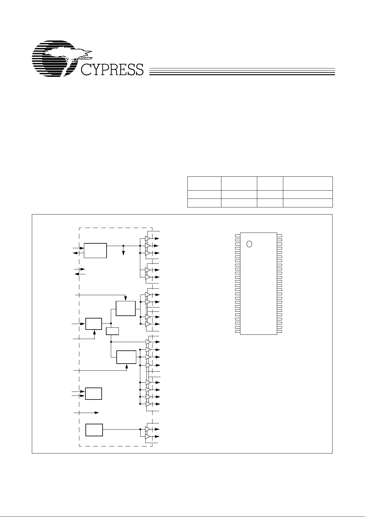
Pin ConfigurationBlock Diagram
VDDREF
REF0/SEL48#
VDDAPIC
APIC0
CPU0
CPU1
CPU2
CPU3
PCI_F
XTAL
PLL Ref Freq
PLL 1
100/66#_SEL
X2
X1
REF1
VDDPCI0
Stop
Clock
Control
Stop
Clock
Control
PCI1
PWR_DWN#
Power
Down
Control
PCI2
PCI3
PCI4
PCI5
48MHz
24/48MHz
PLL2
÷2/÷3
OSC
REF2
VDDCPU0
PCI_STOP#
CPU_STOP#
PCI6
PCI7
GNDPCI1
GND48MHz
VDD48MHz
GNDREF
APIC1
GNDAPIC
GNDCORE0/1
VDDCORE0/1
VDDPCI1
GNDPCI0
GNDCPU1
GNDCPU0
VDDCPU1
SPREAD#
I2C
SDATA
Logic
SCLK
REF0/SEL48#
REF1
GNDREF
X1
X2
GNDPCI0
PCICLK_F
PCI1
VDDPCI0
PCI2
PCI3
GNDPCI1
PCI4
PCI5
VDDPCI1
PCI6
PCI7
GNDPCI2
VDDCORE0
GNDCORE0
VDD48MHz
48MHz
24/48MHz
GND48MHz
VDDREF
REF2
VDDAPIC
APIC0
APIC1
GNDAPIC
NC
VDDCPU0
CPU0
CPU1
GNDCPU0
VDDCPU1
CPUCLK2
CPUCLK3
GNDCPU1
VDDCORE1
GNDCORE1
PCI_STOP#
CPU_STOP#
PWR_DWN#
SPREAD#
SDATA
SCLK
SEL100/66#
48
47
46
45
44
43
42
41
40
39
38
37
36
35
34
33
32
31
30
29
28
27
26
25
1
2
3
4
5
6
7
8
9
10
11
12
13
14
15
16
17
18
19
20
21
22
23
24
Note:
1. Internal pull-up resistors should not be relied upon for
setting I/O pins HIGH.
[1]
Page 2
W48S101-04
PRELIMINARY
2
Pin Definitions
Pin Name Pin No. Pin Type Pin Description
CPU0:3 40, 39, 36,
35
O
CPU Clock Output s 0 through 3:
These four CPU clock outputs are controlled by
the CPU_STOP# control pin. Output voltage sw ing is controll ed by voltage applied
to VDDQ2.
PCI1:7 8, 10, 11,
13, 14, 16,
17
O
PCI Bus Clock Outputs 1 thr ough 7:
These sev en PCI cloc k outputs are control led
by the PCI_STOP# cont rol pin. Output v oltage swing is cont rolled by v oltage applied
to VDDQ3.
PCI_F 7 O
Fixed PCI Clock Output:
Unlike PCI 1:7 o utputs , t his outp ut i s not contr olled b y the
PCI_STOP# control pin. Output voltage swing is controlled by voltage applied to
VDDQ3.
CPU_STOP# 30 I
CPU_STOP# Input:
When brought LO W, clock outputs CPU0:3 are stop ped LOW
after completing a full clock cycle (2–3 CPU clock latency). When brought HIGH,
clock outpu ts CPU0:3 st art beginning wi th a ful l cloc k cycle ( 2–3 CPU clock latency).
PCI_STOP# 31 I
PCI_STOP# Input:
The PCI_STOP# input enables t he PCI 1:7 outputs when HIGH
and causes them to remain at logic 0 when LOW. The PCI_STOP signal is latched
on the rising edge of PCI_F. Its effect takes place on the next PCI_F clock cycle.
SPREAD# 28 I
SPREAD# Input:
When brought LO W th is pin ac tiv at es Sp read Spect rum cloc king.
APIC0:1 45, 44 O
I/O APIC C lock O utputs:
Provides 14. 318-MHz fixe d frequency . The out put volt age
swing is controlled by VDDQ2.
48MHz 22 O
48-MHz Output:
Fixed cloc k outp uts at 48 MHz. Output vol ta ge swi ng is cont ro lled
by voltage applied to VDDQ3.
24/48MHz 23 O
24-MHz or 48-MHz Out put:
24-MHz output when pin 1 is strapped through 10-kΩ
resistor to VDDQ3. 48-MHz output when pin 1 is strapped t hrough 10-k Ω resistor to
GND.
REF0/SEL48# 1 I/O
I/O Dual Function REF0 and SEL48# pin:
During power on, SEL48# input will be
latched, which will set pin 23 to out put 24 MHz or 48 MHz. It then reverts to REF0
fixed output.
REF1:2 2, 47 O
Fixed 14.318-MHz Outputs 1 through 2:
Used for various system applicat ions.
Output voltage swing is controlled by voltage appl ied to VDDQ3.
SEL100/66# 25 I
Frequency Selection Input:
Selects power -up default CPU clock frequency as
shown in Tabl e 1 on page 1.
SCLK 26 I Clock pin for I
2
C circuitry.
SDATA 27 I/O Data pin for I
2
C circuitry.
X1 4 I
Crystal Connection or External Reference Frequency Input:
This pin has dual
functions. It can be used as an external 14.318-MHz crystal connection or as an
external reference frequency i nput.
X2 5 I
Crystal Connection:
An input connection for an external 14.318-MHz crystal. If
using an external reference, this pin must be left unconnected.
PWR_DWN# 29 I
Power Down Contr ol:
When this input is LO W , de vice goe s into a lo w-pow er standby condition. All outputs are actively held LOW while in power-down. CPU and PCI
clock output s are stopped LOW after com pleting a full clock cycle (2–3 CPU clock
cycle latency ). When br ought HI GH, CPU , SDRAM and PCI output s start wi th a fu ll
clock cycle at full operating frequency (3 ms maximum latency).
VDDQ3 9, 15, 19,
21, 33, 48
P
Power Connecti on:
Connect to 3.3V supply.
VDDQ2 46, 41, 37 P
Power Connecti on:
Pow er supply for API C0:1 and CPU0:3 output buf fers. Connect
to 2.5V.
GND 3, 6, 12, 18,
20, 24, 32,
34, 38, 43
G
Ground Connections:
Connect all ground pins to the common system ground
plane.
Page 3
W48S101-04
PRELIMINARY
3
Overview
The W48S101-04, a motherboard clock synthesizer, can provide eith er a 2.5V or 3.3 V CPU clock swing, making it suit able
for a variety of CPU options. A fix ed 48-MHz clock is provided
for oth er syst em func tions . The W48S101 -04 s upports sprea d
spectrum clocking for reduced EMI.
Functional Description
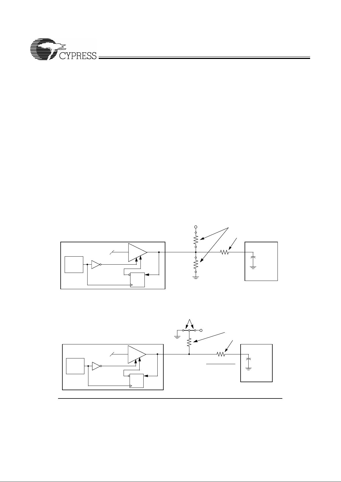
I/O Pin Operation
Pin 1 is a dual-purpose l/O pin. Upon po wer-up this pi n acts as
a logic input, allowing the determination of assigned device
functions . A short time after pow er-up , the logic state of th e pin
is latched and the pin becomes a clock output. This feature
reduces devi ce pin count by combi ning clock out puts with input
select pins .
An external 10-kΩ “strapping” resistor is connected between
the l/O pin and ground or V
DD
. Connection to ground sets a
latch to “0,” connection to V
DD
sets a latch to “1.” Fig ure 1 an d
Figure 2 show two suggested methods for strapping resistor
connections.
Upon W48S101-04 power-up, the first 2 ms of operation is
used for input logic selection. During this period, the Reference clock output buffer is three-stated, allowing the output
strapping resistor on the l/O pin to pull the pin and its associated capacit iv e cloc k load to eith er a l ogic HIGH or LO W stat e .
At the end of the 2-ms period, the established logic “0” or “1”
condition of the l/O pin is then latched. Next the output buffer
is enabled, which converts the l/O pin into an operating clock
output. The 2-ms timer is started when V
DD
reaches 2.0V. The
input bit can only be reset b y turning V
DD
off and then bac k on
again.
It should be noted tha t the stra ppi ng resi stor has no si gnifi cant
effect on clock output signal integri ty. The drive impedance of
clock output is 40Ω (nominal) which is minimally affected by
the 10-kΩ strap to ground or V
DD
. As with th e se r ie s termi n ation resistor, the output strapping resistor should be pla ced as
close to the l/O pin as possible in order to keep the interconnecting trace short. The trace from the resistor to ground or
V
DD
should be kept less than two inches in length to prevent
system noise coupli ng duri ng input logic sampling.
When the clock output is enabled fo ll owing the 2-ms input pe-
riod, a 14.318-MHz output frequency is delivered on the pin,
assuming that V
DD
has stabilized. If VDD has not yet reached
full value , output frequency initi ally ma y be belo w target b ut will
increase to target once V
DD
voltage has stabilized. In either
case, a short output clock cycle may be produced from the
CPU clock outputs when the outputs are enabled.
Power-on
Reset
Timer
Outpu t Three-state
Data
Latch
Hold
QD
W48S101-04
V
DD
Clock Load
10 k
Ω
Output
Buffer
(Load Option 1)
10 k
Ω
(Load Option 0)
Output
Low
Output Strapping Resistor
Series Termination Resistor
Figure 1. Input Logic Selection Through Resistor Load Option
Power-on
Reset
Timer
Output Three-state
Data
Latch
Hold
QD
W48S101-04
V
DD
Clock Load
R
10 k
Ω
Output
Buffer
Output
Low
Output Strapping Resistor
Series Termination Resistor
Jumper Options
Resisto r Value R
Figure 2. Input Logic Selection Through Jumper Option
Page 4
W48S101-04
PRELIMINARY
4
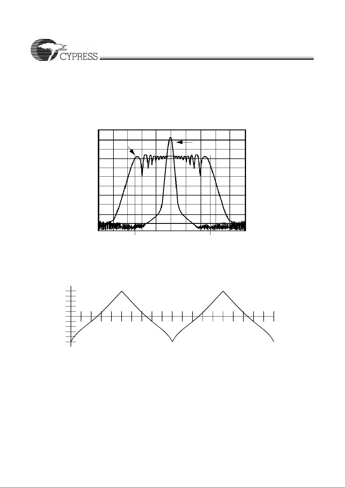
Spread Spectrum Clock Generation
The benefits of using Spr ead Spectrum Clock Generation are
depicted in Figure 3. An EMI emission profile of a clock harmonic is shown.
Contrast the typical clock EMI with the Cy press Spread Spectrum Clock Generation. Notice the spike in the typical clock.
This spike can mak e system s fa il quasi -peak EM I testing . The
FCC and other regulatory agencies test for peak emissions.
With the Cypress clock, the peak energy is much lower (at
least 8 dB) because the energy is spread out across a wider
bandwidth.
Figure 3. Typical Clock and SSCG Comparison
SSFTG Typical Clock
Frequ en cy S p an (M H z)
-SS% +SS%
Amplitude (dB )
5dB/div
MAX (+0.5%)
MIN (–0.5%)
10%
20%
30%
40%
50%
60%
70%
80%
90%
100%
10%
20%
30%
40%
50%
60%
70%
80%
90%
100%
FREQUENCY
Figure 4. Typical Modulation Profile
Page 5

W48S101-04
PRELIMINARY
5
Serial Data Interface
The W48S101-0 4 features a two-pin, serial data interface that
can be used to configure internal register settings that control
particular device functions. Upon power-up, the W48S101-04
initializes wi th default register settings. Therefore, the use of
this serial data interface is optional. The serial interface is
write-only (to the clock chip) and is the dedicated function of
device pins SDATA and SCLOCK. In motherboard applications, SDATA and SCLOCK are typically driven by two logic
outputs of the chipset. Clock device regi ster changes are nor mally made upon system initialization, if required. The interface can also be us ed during system oper ation f or power management functions. Table 2 summarizes the control functions
of the serial data interface.
Operation
Data is written to the W48S101-04 in ten bytes of eight bits
each. Bytes are written in the or der shown in Table 3.
T able 2. Serial Data Interface Control Functions Summary
Control Function Description Common Application
Clock Output Disable Any indivi dual clock output(s) can be disabled. Dis-
abled outputs ar e actively held LO W.
Unused outputs are di sabled to reduce EMI
and system power. Examples are clock outputs to unused PCI slots.
CPU Clock Frequency
Selection
Provides CPU/PCI fr equency selections be yond the
100- and 66.6-MHz sel ecti ons t hat ar e provi ded by
the SEL100/66# pin. Frequency is changed in a
smooth and controlled fashion.
For alternate microprocessors and power
management options . Smooth freque ncy transition allows CPU frequency change under
normal system operation.
Output Three-state Puts all clock outputs into a high-impedance state. Production PCB testing.
T es t Mode All clock out put s toggl e in r elation t o X1 input, int er-
nal PLL is bypassed. Refer to Table 4.
Production PCB testing.
(Reserved) Reserved functio n for future de vice revisi on or pro-
duc tion device testing.
No user application . Regist er bit must be wri t-
ten as 0.
Table 3. Byte Writing Sequence
Byte
Sequence Byte Name Bit Sequence Byte Descr iption
1 Slave Address 11010010 Commands the W48S1 01-04 to accept the bits in Data Bytes 3–6 for
internal registe r configurati on. Since other de vices may exist on the sam e
common serial data b us , it is neces sary to ha v e a sp ecific sl a ve a ddre ss
for each potent ial receiver. The slave receiv er address for the
W48S101-04 is 11010010. Regi ster setting wil l not be made i f the Slav e
Address is not correct (or is for an alternate sla ve receiver).
2 Command
Code
Don’t Care Unused by the W48S101-04, therefore bit v alues are ignored (“don’t
care”). This by te must be include d in the data write seq uence to mainta in
proper byt e allocation. The Command Code Byte is part of the standard
serial communicat ion pr otocol and ma y be used whe n writin g to anoth er
addressed slave receiver on the serial data bus.
3 Byte Count Don’t Care Unused by the W48S101 -04, therefore bit values are ignored (“don’t
care”). This by te must be include d in the data write seq uence to mainta in
proper byt e all ocatio n. The B yte Count Byt e is part of t he stan dard seri al
communication protocol and may be used when writing to another ad-
dressed slave receiver on the serial data bus.
4 Data Byte 0 Don’t Care Refer to Cypress SDRAM drive rs.
5 Data Byte 1
6 Data Byte 2
7 Data Byte 3 Refer to Table 4 The data bits in these bytes set i nternal W48S101-04 regi sters that con-
trol de vice operati on. The data bits ar e only accepted when the Address
Byte bit sequence is 11010010, as noted above. For descri ption of bit
control functions, refer to Table 4, Data Byte Serial Configuration Map.
8 Data Byte 4
9 Data Byte 5
10 Data Byte 6
Page 6

W48S101-04
PRELIMINARY
6
Writing Data Bytes
Each bit in the data bytes controls a pa rticular device fu nction
except f o r the “reserved” bits, which must be written as a logic
0. Bits are written MSB (most significant bit) first, which is bit
7. Table 4 gives the bit formats for registers located in Data
Bytes 3–6.
Ta ble 5 details additional frequency selections that are available through th e seria l dat a interface .
Table 6 details the select functions for Byte 3, bits 1 and 0.
Table 4. Data Bytes 3–6 Seri al Conf iguration Map
Bit(s)
Affected Pin
Control Function
Bit Control
DefaultPin No. Pin Name 0 1
Data Byte 3
7-- --(Reserved) -- -- 0
6 -- -- SEL_2 Refer to Table 5 0
5 -- -- SEL_1 Refer to Table 5 0
4 -- -- SEL_0 Refer to Table 5 0
3 -- -- BYT0_FS# Frequen cy Con trol led
by external SEL100/
66# pin
Frequen cy Con trol led
by BYT0 SEL ( 2:0)
0
2-- --(Reserved) -- -- 0
1–0 -- -- Bit 1 Bit 0 Function (See Table 6 for function details)
0 0 Normal Operation
01Test Mode
1 0 Spread Spectrum on (See Table 5 for frequency and
spread selecti ons. ±0.5% modulation)
1 1 All Outputs Three-stated
00
Data Byte 4
7-- --(Reserved) -- -- 0
6 23 24/48MHz Clock Output Disable Low Active 1
5-- --(Reserved) -- -- 0
4-- --(Reserved) -- -- 0
3 35 CPU3 Clock Output Disable Low Active 1
2 36 CPU2 Clock Output Disable Low Active 1
1 39 CPU1 Clock Output Disable Low Active 1
0 40 CPU0 Clock Output Disable Low Active 1
Data Byte 5
7 7 PCICLK_F Clock Output Disable Low Active 1
6 17 PCI7 Clock Output Disable Low Active 1
5 16 PCI6 Clock Output Disable Low Active 1
4 14 PCI5 Clock Output Disable Low Active 1
3 13 PCI4 Clock Output Disable Low Active 1
2 11 PCI3 Clock Output Disable Low Active 1
1 10 PCI2 Clock Output Disable Low Active 1
0 8 PCI1 Clock Output Disable Low Active 1
Data Byte 6
7-- --(Reserved) -- -- 0
6-- --(Reserved) -- -- 0
5 44 I OAPIC1 Clock Output Disable Low Active 1
4 45 I OAPIC0 Clock Output Disable Low Active 1
3-- --(Reserved) -- -- 0
2 47 REF2 Clock Output Disable Low Active 1
1 2 REF1 Clock Output Disable Low Active 1
0 1 REF0 Clock Output Disable Low Active 1
Page 7

W48S101-04
PRELIMINARY
7
Note:
2. CPU and PCI frequency selections are listed in
Table 1
and
Table 5
.
T able 5. Additional Frequency Selections through Serial Data I nterface Data Bytes
Input Conditions Output Frequency
Data Byte 3, Bit 3 = 1
CPU, SDRAM
Clocks (MHz)
PCI Clocks
(MHz)
Spread Percentage
with Spread Spectrum
turned on
Bit 6
SEL_2
Bit 5
SEL_1
Bit 4
SEL_0
0 0 0 68.5 34.25 ± 0.5% Center
0 0 1 75 37.5 ± 0.5% Center
0 1 0 83.3 41.6 ± 0.5% Center
0 1 1 66.8 33.4 ± 0.5% Center
1 0 0 103 34.33 ± 0.5% Center
1 0 1 112 37.33 ± 0.5% Center
1 1 0 133.3 44.43 ± 0.5% Center
1 1 1 100 33.3 ± 0.5% Center
T able 6. Select Function for Data Byte 3, Bits 0:1
Function
Input Conditions Output Conditions
Data Byte 3
CPU0:3 PCI_F, PCI1:7
REF0:2,
IOAPIC0:1 48MHZ 24MHZBit 1 Bit 0
Normal Operation 0 0 Note 2 Note 2 14.318 MHz 48 MHz 24 MHz
Test Mode 0 1 X1/2 CPU/2, 3, or 4 X1 X1/2 X1/4
Spread Spectrum On 1 0 Note 2,
55%±0.5
Note 2,
55%±0.5
14.318 MHz 48 MHz 24 MHz
Three-state 1 1 Hi-Z Hi-Z Hi-Z Hi-Z Hi-Z
Page 8

W48S101-04
PRELIMINARY
8
Absolute Maximum Ratings
Stresses gre ater th an those list ed i n this tab le may cause permanent damage to the de vice. These represent a str ess ratin g
only. Operation of the device at these or any other conditions
above those specified in the operatin g sections of this specification is not implied. Maximum conditions for extended periods may affect reliability.
Parameter Description Rating Unit
V
DD
, V
IN
V oltage on any pin with respect to GND –0.5 to +7 .0 V
T
STG
Storage Temperature –65 to +150 °C
T
A
Operating Temperature 0 to +70 °C
T
B
Ambient Temperature under Bias –55 to +125 °C
ESD
PROT
Input ESD Protection 2 (min.) kV
DC Electr i cal C h ar acteristics :
TA = 0°C to +70°C, V
DDQ3
= 3.3V±5%, V
DDQ2
= 2.5V±5%
Parameter Description Test Condition Min. Typ. Max. Unit
Supply Current
I
DDQ3
3.3V Supply Current CPUCLK =100 MHz
Outputs Loaded
[3]
120 mA
I
DDQ3
2.5V Supply Current 60 mA
Logic Inputs
V
IL
Input Low V oltage GND –
0.3
0.8 V
V
IH
Input High V oltage 2.0 VDD +
0.3
V
I
IL
Input Low Current
[4]
–25 µA
I
IH
Input High Current
[4]
10 µA
I
IL
Input Low Current (SEL100/66#) –5µA
I
IH
Input High Current (SEL100/66#) 5 µA
Clock Outputs
V
OL
Output Low Voltage IOL = 1 mA 50 mV
V
OH
Output High Voltage IOH = –1 mA 3.1 V
V
OH
Output High Voltage (CPU, APIC) IOH = –1 mA 2.2 V
I
OL
Output Low Current CPU0:3 V
OL
= 1.25V 27 57 97 mA
PCI_F, PCI1:7 V
OL
= 1.5V 20.5 53 139 mA
APIC0:1 V
OL
= 1.25V 40 85 140 mA
REF0:2 V
OL
= 1.5V 25 37 76 mA
48MHz 0:1 V
OL
= 1.5V 25 37 76 mA
I
OH
Output High Current CPU0:3 V
OL
= 1.25V 25 55 97 mA
PCI_F, PCI1:7 V
OL
= 1.5V 31 55 189 mA
APIC0:1 V
OL
= 1.25V 40 87 155 mA
REF0:2 V
OL
= 1.5V 27 44 94 mA
48MHz 0:1 V
OL
= 1.5V 27 44 94 mA
Notes:
3. All clock outputs loaded with maximum lump capacitance test load specified in the AC Electrical Characteristics section.
4. W48S101-04 logic inputs have internal pull-up devices, except SEL100/66#.
Page 9

W48S101-04
PRELIMINARY
9
AC Electrical Characteristics
T
A
= 0°C to +70°C, V
DDQ3
= 3.3V±5%,V
DDQ2
= 2.5V± 5%, f
XTL
= 14.31818 MHz
AC clock parameters are tested and guaranteed over stated operating conditions using the stated lump capacitive load at the
clock output; Spread Spect rum clocking is disabled.
Notes:
5. X1 input threshold voltage (typical) is V
DD
/2.
6. The W48S101-04 contains an internal crystal load capacitor between pin X1 and ground and another between pin X2 and ground. Total load placed on crystal
is 14 pF; this includes typical stray capacitance of short PCB traces to crystal.
7. X1 input capacitance is applicable when driving X1 with an external clock source (X2 is left unconnected).
Crystal Oscillator
V
TH
X1 Input Threshold Voltage
[5]
1.5 V
C
LOAD
Load Capacitance, as seen by
External C rys tal
[6]
14 pF
C
IN,X1
X1 Input Capacitance
[7]
Pin X2 unconnected 28 pF
Pin Capacitance/Induct ance
C
IN
Input Pin Capacitance Except X1 and X2 5 pF
C
OUT
Output Pin Capacitance 6 pF
L
IN
Input Pin Inductance 7nH
DC Electr i cal C h ar acteristics :
TA = 0°C to +70°C, V
DDQ3
= 3.3V±5%, V
DDQ2
= 2.5V±5% (continued)
Parameter Description Test Condition Min. Typ. Max. Unit
CPU Clock Outputs, CPU0:3 (Lump Capacitance Test Load = 20 pF)
Parameter Description Test Condition/Comments
CPU = 66.8 MHz CPU = 100 MHz
UnitMin. Typ. Max. Min. Typ. Max.
t
P
Period Measured on rising edge at 1. 25V 15 15.5 10 10.5 ns
t
H
High Time Duration of clock cycle above 2.0V 5.2 3.0 ns
t
L
Low Time Duration of clock cycle below 0.4V 5.0 2.8 ns
t
R
Output Rise Edge Rate Measured from 0.4V to 2.0V 1 4 1 4 V/ns
t
F
Output Fall Edge Rate Measured from 2.0V to 0.4V 1 4 1 4 V/ns
t
D
Duty Cycle Measured on rising and falling edge at
1.25V
45 55 45 55 %
t
JC
Jitter , Cycle-to-Cycle Measured on rising edge at 1.25V. Max-
imum differ ence of cycle time bet w een
two adjacent cycles.
200 250 ps
t
SK
Output Skew Measured on rising edge at 1. 25V 175 175 ps
f
ST
Frequency Stabilization from Po wer-up
(cold start)
Assumes full supply voltage reached
within 1 ms from power-up . Short cycles
exist prior to frequency stabilizat ion.
33ms
Z
o
AC Output Impedance Average value during switching transi-
tion. Used for dete rmini ng series terminat i o n value.
20 20 Ω
Page 10

W48S101-04
PRELIMINARY
10
PCI Clock Outputs, PCI1:7 and PCI_F (L ump Capacitance Test Load = 30 pF
Parameter Description Te st Condi tion/Comments
CPU = 66.8/100 MHz
UnitMin. Typ. Max.
t
P
Period Measured on rising edge at 1.5V 30 ns
t
H
High Time Duration of clock cycle abov e 2.4V 12 ns
t
L
Low Time Duration of clock cycle bel ow 0.4V 12 ns
t
R
Output Rise Edge Rate Measured from 0.4V to 2.4V 1 4 V/ns
t
F
Output Fall Edge Rate Measured from 2.4V to 0.4V 1 4 V/ns
t
D
Duty Cycle Measured on rising and falling edge at 1.5V 45 55 %
t
JC
Jitter , Cycle-to-Cycle Measured on rising edge at 1.5V. Maximum
differ ence of cyc le time be tween tw o adjacent cycles .
250 ps
t
SK
Output Skew Measured on rising edge at 1.5V 500 ps
t
O
CPU to PCI Clock Skew Covers all CPU/PCI outputs. Measured on r ising
edge at 1.5V. CPU leads PCI output.
1.5 4 ns
f
ST
Frequency Stabilization
from Power-up (cold
start)
Assumes full supply voltage reached within 1 ms
from power-up. Short cycles exist prior to frequency
stabilization.
3ms
Z
o
AC Output Impeda nce Average value during switching transition. Used for
determining series termination value.
30 Ω
APIC0:1 Clock Output (Lump Capacitance Test Load = 20 pF)
Parameter Description Test Condi tion/Comments
CPU = 66.8/100 MHz
UnitMin. Typ. Max.
f Frequency, Actual Frequency generated by crystal oscillator 14.31818 MHz
t
R
Output Rise Edge Rate Measur ed fr om 0.4V to 2.0V 1 4 V/ns
t
F
Output Fal l Edge Rate Measured from 2.0V to 0.4V 1 4 V/ns
t
D
Duty Cycle Measured on rising and falling edge at 1.25V 45 55 %
f
ST
Frequency Stabilization
from Power-up (cold start)
Assumes full supply voltage reached within
1 ms from power-up . Sh ort cycles exist prior to
frequency stabi li zation.
1.5 ms
Z
o
AC Output Impedance Av erage value during s witching transi tion. Used
for determining seri es termi nation value.
15 Ω
REF0:2 Clock Output (Lump Capacit ance Test Load = 20 pF)
Parameter Description Test Condition/Comments
CPU = 66.8/100 MHz
UnitMin. Typ. Max.
f Frequency, Actual Frequency generated by crystal oscillator 14.318 MHz
t
R
Output Rise Edge Rate Measured from 0.4V to 2.4V 0.5 2 V/ns
t
F
Output Fall Edge Rate Measured from 2.4V to 0.4V 0.5 2 V/ ns
t
D
Duty Cycle Measured on rising and falling edge at 1.5V 45 55 %
f
ST
Frequency St abilization from
Power-up (cold start)
Assumes full supply voltage reached within
1 ms from power-up. Short cycles exist prior to
frequency stabi li zation.
3ms
Z
o
AC Output Impedance Av erage val ue during switchi ng transition. Used
for determining seri es termination value.
40 Ω
Page 11

W48S101-04
PRELIMINARY
11
Document #: 38-00853
48MHz0:1 Clock Output (Lump C apacitance Test Load = 20 pF = 66.6/100 MHz)
Parameter Description Test Condition/Comments
CPU = 66.8/100 MHz
UnitMin. Typ. Max.
f Frequency, Actual Determined by PLL divider rat io (see m/n below) 48.008 MHz
f
D
Deviation from 48 MHz (48.008 – 48)/48 +167 ppm
m/n PLL Ratio (14.31818 MHz x 57/17 = 48.008 MHz) 57/17
t
R
Output Rise Edge Rate Measur ed fr om 0.4V to 2.4V 0.5 2 V/ns
t
F
Output Fall Edge Rate Measured from 2.4V to 0.4V 0.5 2 V/ns
t
D
Duty Cycle Measured on rising and falling edge at 1.5V 45 55 %
f
ST
Frequency Stabilization
from Power-up (cold start)
Assumes full supply vol tage reached withi n 1 ms
from power-up. Short cycles exist prior to frequency stabilization.
3ms
Z
o
AC Output Impedance Average value dur ing switching transition. Used
for determining seri es termi nation value.
40 Ω
Ordering Information
Ordering Code
Freq. Mask
Code
Package
Name Package Type
W48S101 -04 H 48-pin SSOP (300 mils)
Page 12

W48S101-04
PRELIMINARY
© Cypress Semiconductor Corporation, 1999. The information contained herein is subject to change without notice. Cypress Semiconductor Corporation assumes no responsibility for the use
of any circuitry other than circuitry embodied in a Cypress Semiconductor product. Nor does it con vey or imply any license under patent or other rights. Cypress Semiconductor does not authorize
its products for use as critical components in life-support systems where a malfunction or failure may reasonably be expected to result in significant injury to the user. The inclusion of Cypress
Semiconductor products in life-support systems application implies that the manufacturer assumes all risk of such use and in doing so indemnifies Cypress Semiconductor against all charges.
Package Diagram
48-Pin Small Shrink Outlin e P ackage (SSOP, 300 mils)
Summary of nominal di mensions in inches:
Body Width: 0.296
Lead Pitch: 0.025
Body Length: 0.625
Body Height: 0.102
 Loading...