

Page 1
PRELIMINARY
100-MHz Mobile Motherboard System Clock
W48C111-17
Cypress Semiconductor Corporation
• 3901 North First Street • San Jose • CA 95134 • 408-943-2600
Novembe r 2, 1999, rev. **
Features
• Maximized EMI suppression usi ng Cypress’s Spread
Spec t r u m techno logy
• Power-on default to spread mode
• T wo copies of CPU output
• Six copies of PCI output (synchr onous w/CPU outputs)
• One copy of 48-MHz USB output
• One Buffered copy of 14.318-MHz input reference signal
• Supports 100-MHz or 66-MHz CPU operation
• Power man agem ent control input pins
• Low Frequency Test Mode
• Av ail able in 28-pin SSOP (209 mil)
Key Specific ati o n s
Supply Voltages:.......................................V
DDQ3
= 3.3V±5%
V
DDQ2
= 2.5V±5%
CPU0: 1 S kew: ....... ... ......... ... .. .......... .. ... ......... ... .. .......175 p s
CPU0: 1 C y cl e- to - C yc le Ji tt er: ....................... .. ... .........20 0 p s
PCI_ F, PCI1:5 Skew : ..... ... .. .......... .. ... .......... .. .............. 5 0 0 ps
PCI_ F, PCI1:5 Cyc le -to-Cycl e Jit te r: . .. .......... .. ... .........250 p s
CPU to PCI Skew: ........................ 1.5 to 4.0 ns (CPU Leads)
Output Duty Cycle: .................................................... 45/55%
PCI_F, PCI Edge Rate :.............................. ............... .>
1 V/ns
CPU_STOP#, PWR_DWN#, PCI_STOP#: 250-kΩ pull-up
resistor
T able 1. Pin Selectable Frequency
SEL100/66# CPU(0:1) PCI Spread%
0 66.6 MHz 33.3 –0.5%
1 100 MHz 33.3 –0.5%
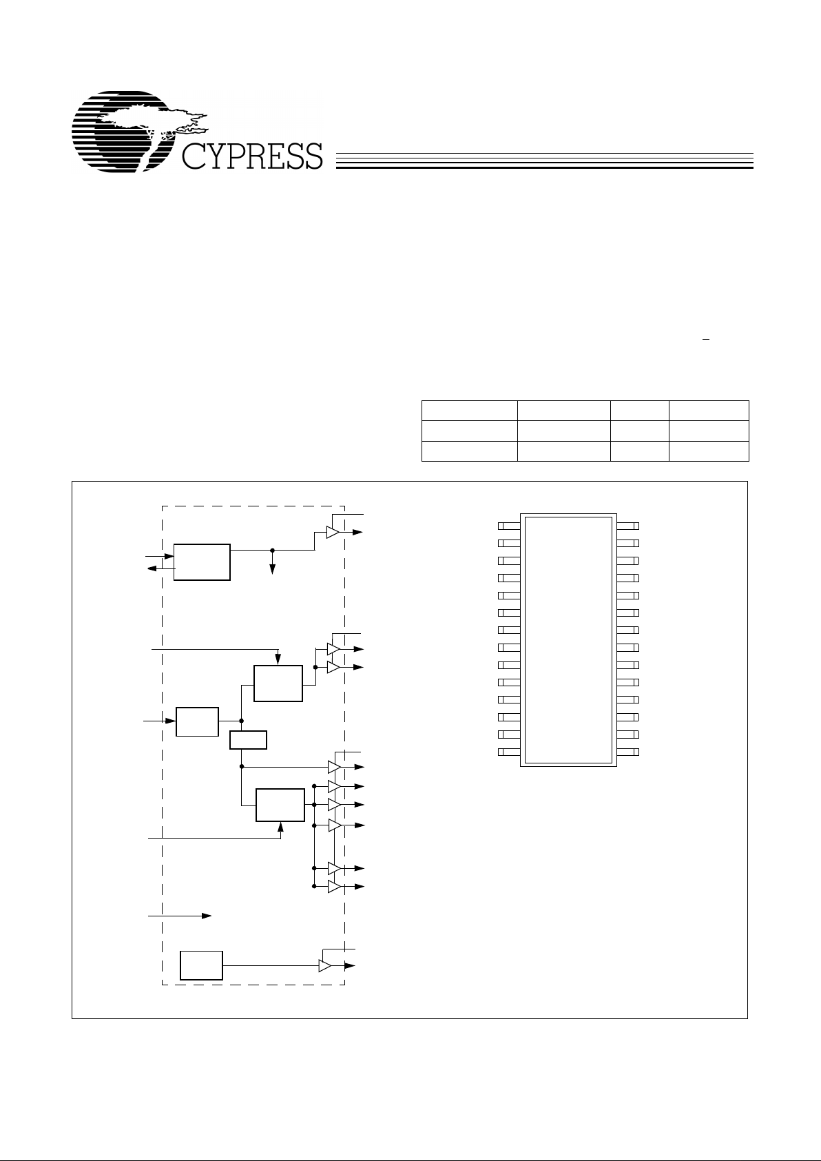
Pin ConfigurationBlock Diagram
GND
VDDQ3
REF
VDDQ2
CPU0
CPU1
GND
VDDQ3
GND
PCI_STOP#
CPU_STOP#
PWR_DWN#
48MHz
SEL100/66#
28
27
26
25
24
23
22
21
20
19
18
17
16
15
X1
X2
GND
PCI_F
PCI1
VDDQ3
PCI2
PCI3
VDDQ3
PCI4
PCI5
GND
VDDQ3
GND
1
2
3
4
5
6
7
8
9
10
11
12
13
14
VDDQ3
REF
CPU0
CPU1
PCI_F
XTAL
PLL Ref Freq
PLL 1
SEL100/66#
X2
X1
VDDQ3
Stop
Signal
Control
Stop
Signal
Control
PCI1
PWR_DWN#
Power
Down
Control
PCI2
PCI3
PCI4
PCI5
÷2/÷3
OSC
VDDQ2
PCI_STOP#
CPU_STOP#
PLL 2
48MHz
VDDQ3
Page 2
W48C111-17
PRELIMINARY
2
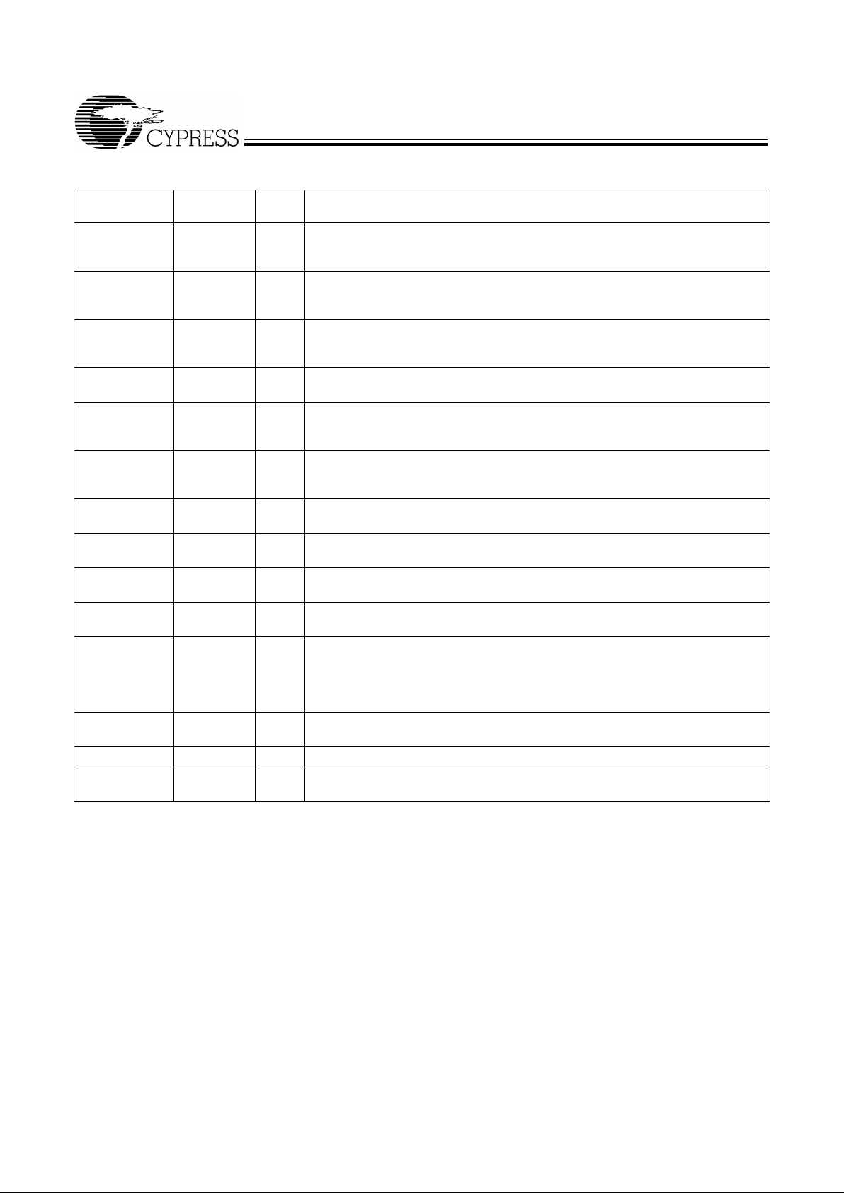
Pin Definitions
Pin Name
Pin
No.
Pin
Ty pe Pin Description
CPU0:1 24, 23 O
CPU Clock Outputs 0 and 1:
These two CPU clock out puts are controlled by th e
CPU_STOP# control pin. Output volta ge swing is controlle d by voltage applied to
VDDQ2. Frequency of signals is set by SEL100/66# input.
PCI1:5 5, 7 , 8 , 10, 11O
PCI Bus Clock Outputs 1 through 5:
These five PCI clock outputs are controlled
by the PCI _ST OP# contr ol p in. Outpu t v ol tage s wing is co ntr olled b y v olt age applied
to VDDQ3.
PCI_F 4 O
Fixed PCI Clock Output:
Unlike PCI1:5 outputs, this output is not controlled by the
PCI_STOP# control pin; it cannot be forced LOW by PCI_STOP#. Output voltage
swing is controlled by voltage applied to VDDQ3.
48MHz 16 O
48-MHz Output:
Fixed cloc k output at 48 MHz. Out put vol tage swi ng is contr olled b y
voltage applied to VDDQ3.
CPU_STOP# 18 I
CPU_STOP# Input:
When brought LOW, clock outputs CPU0:1 are stopped LOW
after completi ng a full clock cycl e (2–3 CPU clock latency). When brought HIGH,
clock outputs CPU0:1 start with a full clock cycle (2–3 CPU cl o ck l a te ncy).
PCI_STOP# 19 I
PCI_STOP# Input:
The PCI_STOP # input enables the PCI1:5 outputs when HIGH
and causes them to remain at logi c 0 when LOW. The PCI_STOP signal is latched
on the rising edge of PCI_F. Its effect takes place on the next PCI_F clock cycle.
REF 26 O
Fixed 14.318-MHz Output:
Used for various system applications. Output voltage
swing is controlled by voltage applied to VDDQ3.
SEL100/66# 15 I
Frequency Selection Inputs:
Select power -up default CPU clock frequency as
shown in Table 1 on page 1.
X1 1 I
Crystal Connection or External Reference Frequency Input:
This pin can either
be used as a connection to a crystal or to a reference signal.
X2 2 I
Crystal Connection:
An input connection for an external 14.318-MHz crystal. If
using an external reference, this pin must be left unconn ected.
PWR_DWN# 17 I
Power- Down Control:
When this input is LO W, de vi ce goes in to a l ow-po wer standby conditio n. All outputs are held LO W. CPU and PCI clock outputs are st opped LOW
after completi ng a full clock cycl e (2–3 CPU clock cycle latency). When brought
HIGH, CPU and PCI outputs start with a full cloc k cycle at full operating f requency
(3 ms maximum latency).
VDDQ3 6, 9, 13, 21, 27P
Power Connecti on:
Connected to 3.3V supply.
VDDQ2 25 P
Power Connecti on:
Power supply for CPU0:1 output buffer. Connected to 2.5V.
GND 3, 12, 14, 20,
22, 28
G
Ground Connection:
Connect all gro und pins t o the common s yst em g round pl an e.
Page 3
W48C111-17
PRELIMINARY
3
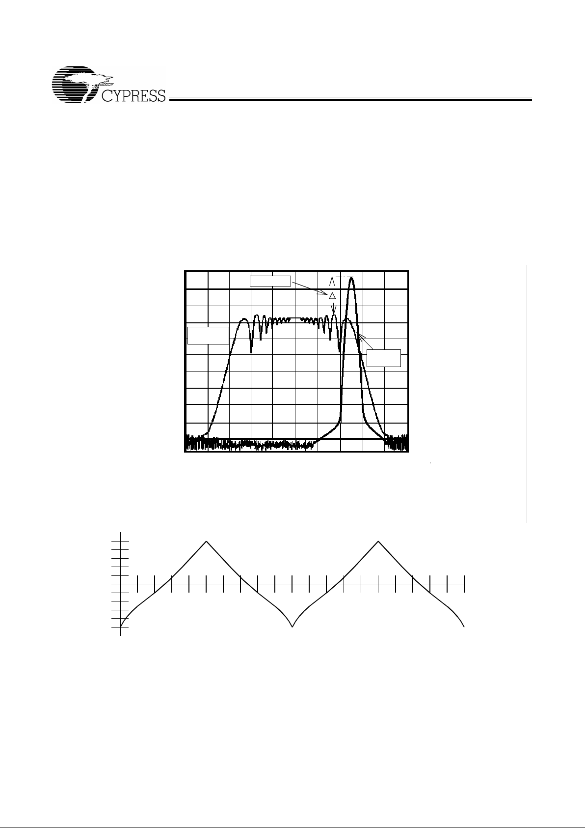
Spread Sp ectrum Feat u re
The device generates a clock that is frequency modulated in
order to increase the bandwidth that it occu pies. By increas ing
the bandwidth of the fundamental and its harmonics, the amplitudes of the radiated electromagnetic emissions are reduced. This effect is depicted in Figure 1.
As shown in Figure 1, a harmonic of a modulated clock has a
much low er amplitude th an that of an un modulated si gnal. The
reduction in amplitude is dependent on the harmonic number
and the frequency deviation or spread. The equation for the
reduction is:
dB = 6.5 + 9*log
10
(P) + 9*log10(F)
Where P is the perce nta ge of de viati on and F is the frequen cy
in MHz where the reduction is measured.
The output clock is modulated with a waveform depicted in
Figure 2. This waveform, as discussed in “Spread Spectrum
Clock Generation f or the Reducti on of Radiated Emissio ns” by
Bush, Fessler, and Hardin produces the maximum reduction
in the amplitude of radiated electromagnetic emissions. The
deviati on select ed for this chi p is –0.5% of the cente r frequency. Figure 2 details the Cypress spreading pattern. Cypress
does offer options with more spread and greater EMI reduction. Contact your local Sales representative for details on
these devices.
Spread
Spectrum
Enabled
EMI Reduction
Spread
Spectrum
Non-
Figure 1. Typi cal Clock and SSFTG Compari son
MAX (+0.5%)
MIN (–0.5%)
10%
20%
30%
40%
50%
60%
70%
80%
90%
100%
10%
20%
30%
40%
50%
60%
70%
80%
90%
100%
FREQUENCY
Figure 2. Typica l Modulation Profile
Page 4

W48C111-17
PRELIMINARY
4
Absolute Maximum Ratings
Stresses gre ater th an those list ed i n this tab le may cause permanent damage to the de vice. These represent a str ess ratin g
only. Operation of the device at these or any other conditions
above those specified in the operating sect ions of this spec if ication is not implied. Maximum conditions for extended periods may affect reliability.
Parameter Description Rating Unit
V
DD
, V
IN
V oltage on any pin with respect to GND –0.5 to +7.0 V
T
STG
Storage Temperature –65 to +150 °C
T
A
Operating Temperature 0 to +70 °C
T
B
Ambient Temperature under Bias –55 to +125 °C
ESD
PROT
Input ESD Protection 2 (min.) kV
DC Electr i cal C h ar acteristics :
TA = 0°C to +70°C, V
DDQ3
= 3.3V±5%, V
DDQ2
= 2.5V±5%, CPU0:1 = 66.6/100 MHz
Parameter Description Test Condition Min. Typ. Max. Unit
Supply Current
I
DD
3.3V Supply Current Outputs Loaded
[1]
75 mA
I
DD
2.5 2.5V Supply Current Outputs Loaded
[1]
50 mA
Logic Inputs
V
IL
Input Low Voltage GND – 0.3 0.8 V
V
IH
Input High Voltage 2.0 VDD + 0.3 V
I
IL
Input Low Current
[2]
–25 µA
I
IH
Input High Current
[2]
10 µA
I
IL
Input Low Current (SEL10 0/66#) –5µA
I
IH
Input High Current (SEL100/66#) 5 µA
Clock Outputs
V
OL
Output Low Voltage IOL = 1 mA 50 mV
V
OH
Output High Voltage IOH = –1 mA 3.1 V
V
OH
Output High Voltage CPU0:1 IOH = –1 mA 2.2 V
I
OL
Output Low Current CPU0:1 V
OL
= 1.25V 55 115 190 mA
PCI1:5, _ F V
OL
= 1.5V 20.5 53 139 mA
REF V
OL
= 1.5V 25 37 76 mA
I
OH
Output High Current CPU0:1 V
OL
= 1.25V 50 110 195 mA
PCI1:5, _ F V
OL
= 1.5V 31 55 189 mA
REFX V
OL
= 1.5V 27 44 94 mA
Crystal Oscillator
V
TH
X1 Input Threshold Voltage
[3]
V
DDQ3
= 3.3V 1.65 V
C
LOAD
Load Capacitance, as seen by External Crystal
[4]
14 pF
C
IN,X1
X1 Input Capacitance
[5]
Pin X2 unconnected 28 pF
Pin Capacitance/Induct ance
C
IN
Input Pin Capacitanc e Except X1 and X2 5 pF
C
OUT
Output Pin Capacitance 6pF
L
IN
Input Pin Inductance 7nH
Notes:
1. All clock outputs loaded with 6" 60Ω transmission lines with 20-pF capacitors.
2. CPU_STOP#, PCI_STOP#, and PWRDWN# logic inputs have internal pull-up resistors.
3. X1 input threshold voltage (typical) is V
DD
/2.
4. The W48C111-17 contains an internal crystal load capacitor between pin X1 and ground and another between pin X2 and ground. T otal load placed on crystal
is 14 pF; this includes typical stray capacitance of short PCB traces to crystal.
5. X1 input capacitance is applicable when driving X1 with an external clock source (X2 is left unconnected).
Page 5

W48C111-17
PRELIMINARY
5
AC Electrical Characteristics
T
A
= 0°C to +70°C, V
DDQ3
= 3.3V±5%,V
DDQ2
= 2.5V± 5%, f
XTL
= 14.31818 MHz
AC clock parameters are tested and guaranteed over st ated operating conditions using the stated lump capacitive load at the
clock o utput.
CPU Clock Outputs, CPU0:1 (Lump Capacitance Test Load = 20 pF)
Parameter Description Test Conditi on/Comments
CPU = 66.6 MHz CPU = 100 MHz
UnitMin. Typ. Max. Min. Typ. Max.
t
P
Period Measured on rising edge at 1.25V 15 15.5 10 10.5 ns
t
H
High Time Duration of clock cycle above 2.0V 5.2 3.0 ns
t
L
Low Time Duration of clock cycle below 0.4V 5.0 2.8 ns
t
R
Output Rise Edge Rate Me asured from 0.4V to 2.0V 1 4 1 4 V/ns
t
F
Output Fall Edge Time Measured from 2.0V to 0.4V 1 4 1 4 V/ns
t
D
Duty Cycle Measured on rising and falling edge at
1.25V
45 55 45 55 %
t
JC
Jitter , Cycle-to-Cycle Measured on rising edge at 1.25V. Max-
imum differ ence of cycle time bet w een
two adjacent cycles.
200 250 ps
t
SK
Output Skew Measured on rising edge at 1.25V 175 175 ps
f
ST
Frequency Stabilization from Po wer-up
(cold start)
Assumes full supply voltage reached
within 1 ms from power-up . Short cycles
exist prior to frequency stabilizat ion.
33ms
Z
o
AC Output Impedance Average value during switching transi-
tion. Used for dete rmini ng series terminat i o n value.
13.5 13.5 Ω
PCI Clock Outputs, PCI1:5 and PCI_F (L ump Capacitance Test Load = 30 pF
Parameter Description Te st Condi tion/Comments
CPU = 66.6/100 MHz
UnitMin. Typ. Max.
t
P
Period Measured on rising edge at 1.5V 30 ns
t
H
High Time Duration of cl ock cycle above 2.4V 12 ns
t
L
Low Time Duration of clock cycle below 0.4V 12 ns
t
R
Output Rise Edge Rate Measured from 0.4 V to 2.4 V 1 4 V/ns
t
F
Output Fall Edge Rate Measured from 2.4V to 0.4V 1 4 V/ns
t
D
Duty Cycle Measured on rising and fa ll ing edge at 1.5V 45 55 %
t
JC
Jitter , Cycle-to-Cycle Measured on risi ng edge at 1.5V. Maximum
differ ence of cyc le time be tween tw o adjacent cycles .
250 ps
t
SK
Output Skew Measured on rising edge at 1.5V 500 ps
t
O
CPU to PCI Clock Skew Covers all CPU/PCI outputs. Measured on rising
edge at 1.5V. CPU leads PCI output.
1.5 4 ns
f
ST
Frequency Stabilization
from Power-up (cold
start)
Assumes full supply voltage reached within 1 ms
from power-up. Short cycles exist prior to frequency
stabilization.
3ms
Z
o
AC Output Impeda nce Average value during switching transiti on. Used for
determining series termination value.
30 Ω
Page 6

W48C111-17
PRELIMINARY
6
Document #:38-00843
REF Clock Output (Lump Capacitance Test Load = 20 pF)
Parameter Description Test Condition/Comments
CPU = 66.6/100 MHz
UnitMin. Typ. Max.
f Frequency, Actual Frequency generated by crystal oscillator 14.318 MHz
t
R
Output Rise Edge Rate Measured from 0.4V to 2.4V 0.5 2 V/ns
t
F
Output Fal l Edge Rate Measured from 2.4V to 0.4V 0.5 2 V/ns
t
D
Duty Cycle Measured on rising and falling edge at 1.5V 45 55 %
f
ST
Frequency St abilization from
Power-up (cold start)
Assumes full supply voltage reached within 1 ms
from power-up. Short cycles exist prior to
frequency stabi li zation.
3ms
Z
o
AC Output Impedance A verage val ue during switching t ransition. Used f or
determining series termination value.
40 Ω
48-MHz Clock Output (Lump Capacit ance T est Load = 20 pF)
Parameter Description Test Condition/Comments
CPU = 66.6/100 MHz
UnitMin. Typ. Max.
f Freque ncy, Actual Determined by PLL divider ratio (see m/n below) 48.008 MHz
f
D
Deviation from 48 MHz (48.008 – 48)/4 8 +167 ppm
m/n PLL Ratio (14.31818 MHz x 57/17 = 48.008 MHz) 57/17
t
R
Output Rise Edge Rate Measured from 0.4V to 2.4V 0.5 2 V/ns
t
F
Output Fall Edge Rate Measured from 2.4V to 0.4V 0.5 2 V/ns
t
D
Duty Cycle Measured on rising and falling edge at 1.5V 45 55 %
f
ST
Frequency Stabilization
from Power-up (cold start)
Assumes full supply vol tage reached withi n 1 ms
from power-up. Short cycles exist prior to frequency stabilization.
3ms
Z
o
AC Output Impedance Average value during switching transition. Used
for determining seri es termi nation value.
40 Ω
Ordering Information
Ordering Code
Freq. Mask
Code
Package
Name Package Type
W48C111 -17 H 28-pin SSOP (209 mils)
Page 7

W48C111-17
PRELIMINARY
© Cypress Semiconductor Corporation, 1999. The information contained herein is subject to change without notice. Cypress Semiconductor Corporation assumes no responsibility for the use
of any circuitry other than circuitry embodied in a Cypress Semiconductor product. Nor does it con vey or imply any license under patent or other rights. Cypress Semiconductor does not authorize
its products for use as critical components in life-support systems where a malfunction or failure may reasonably be expected to result in significant injury to the user. The inclusion of Cypress
Semiconductor products in life-support systems application implies that the manufacturer assumes all risk of such use and in doing so indemnifies Cypress Semiconductor against all charges.
Package Diagram
28-Pin Small Shrink Outlin e P ackage (SSOP, 209 mils)
 Loading...