

Page 1
PRELIMINARY
Spread Spectrum BX System Frequency Generator
W48C101-01
Cypress Semiconductor Corporation
• 3901 North First Street • San Jose • CA 95134 • 408-943-2600
October 7, 1999, rev. **
Features
• Maximized EMI suppression usi ng Cypress’s Spread
Spec t r u m techno logy
• Four copies of CPU output
• Eight copies of PCI output (Synchronous w/CPU
output)
• T wo copies of 14.318-MHz IO APIC output
• T wo copies of 48-MHz USB output
• Three buffered copies of 14.318-MHz reference input
• Input is a 14.318-MHz XTAL or reference signal
• Selectable 100- M Hz or 66-MHz CPU outputs
• Power man agem ent control input pins
• T est mode and output three-state capability
Key Specific ati o n s
Supply Voltages:.......................................V
DDQ3
= 3.3V±5%
V
DDQ2
= 2.5V±5%
CPU0:3 Jitter (Cycl e to Cycle):................................... 200 ps
CPU0: 3 C lo ck Skew: .................... .. .................... .. ... .... 1 7 5 ps
PCI_ F, PCI1:7 Cl o ck Skew: ..... ... ......... ... .. .......... .. ... ....500 ps
CPU to PCI Clock Skew: ....... .. .....1.5 to 4.0 ns (CPU L e ad s )
Logic inpu ts have 250-kΩ pull-up resistors e xcept SEL100/66 #.
T able 1. Pin Selectable Frequency
SEL
100/66# SEL1 SEL0
CPU
(MHz)
PCI
(MHz) SPREAD#=0
0 0 0 HI-Z HI-Z Don’t Care
0 0 1 66.6 33.3 ±0.9% Center
0 1 0 66.6 33.3 –1% Down
0 1 1 66.6 33.3 –0.5% Down
1 0 0 X1/2 X1/6 Don’t Care
1 0 1 100 33.3 ±0.9% Center
1 1 0 100 33.3 –1% Down
1 1 1 100 33.3 –0.5% Down
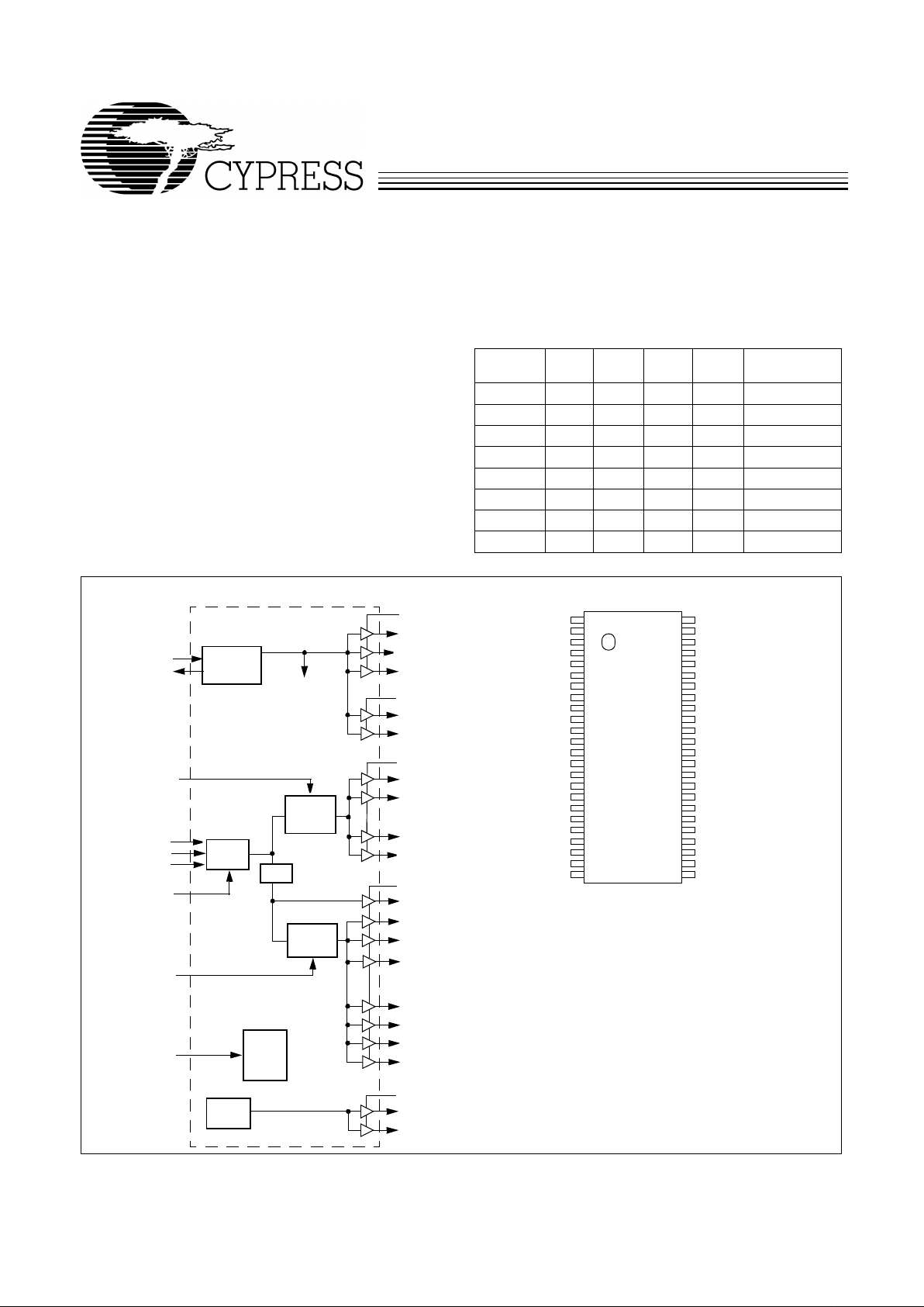
Pin ConfigurationBlock Diagram
REF0
REF1
GND
X1
X2
GND
PCI_F
PCI1
VDDQ3
PCI2
PCI3
GND
PCI4
PCI5
VDDQ3
PCI6
PCI7
GND
VDDQ3
GND
VDDQ3
48MHz
48MHz
GND
VDDQ3
REF2
VDDQ2
APIC0
APIC1
GND
NC
VDDQ2
CPU0
CPU1
GND
VDDQ2
CPU2
CPU3
GND
VDDQ3
GND
PCI_STOP#
CPU_STOP#
PWR_DWN#
SPREAD#
SEL0
SEL1
SEL100/66#
48
47
46
45
44
43
42
41
40
39
38
37
36
35
34
33
32
31
30
29
28
27
26
25
1
2
3
4
5
6
7
8
9
10
11
12
13
14
15
16
17
18
19
20
21
22
23
24
VDDQ3
REF0
VDDQ2
APIC0
CPU0
CPU1
CPU2
CPU3
PCI_F
XTAL
PLL Ref Freq
PLL 1
SEL100/66#
X2
X1
REF1
VDDQ3
Stop
Clock
Control
Stop
Clock
Control
PCI1
PWR_DWN#
Power
Down
Control
PCI2
PCI3
PCI4
PCI5
48MHz
48MHz
PLL2
÷2/÷3
OSC
REF2
VDDQ2
PCI_STOP#
CPU_STOP#
PCI6
PCI7
VDDQ3
APIC1
SEL0
SEL1
SPREAD#
Page 2
W48C101-01
PRELIMINARY
2
Pin Definitions
Pin Name
Pin
No.
Pin
Type Pin Description
CPU0:3 40, 39, 36,
35
O
CPU Clock Output s 0 through 3:
These four CPU clock outputs are controlled b y
the CPU_STO P# contr ol pin . Output vol tage swing is cont roll ed by v oltag e appli ed
to VDDQ2.
PCI1:7 8, 10, 11, 13,
14, 16, 17
O
PCI Bus Clock Outputs 1 thr ough 7:
These sev en PCI clock outputs are cont rolled
by the PCI _STOP# con trol pin. Out put volt age swing is controlle d by v oltage applie d
to VDDQ3.
PCI_F 7 O
Fixed PCI Clock Output:
Unlike PCI 1:7 outputs , this output i s not cont rolled by the
PCI_STOP# control pin. Output voltage swing is controlled by voltage applied to
VDDQ3.
CPU_STOP# 30 I
CPU_STOP# Input :
When brought LO W, c lock output s CPU0: 3 are s topped LO W
after completing a full clock cycle (2–3 CPU clock latency). When brought HIGH,
clock out puts CPU0:3 start beginn ing with a full clock cyc le (2–3 CPU clock latency).
PCI_STOP# 31 I
PCI_STOP# I nput:
The PCI_STOP# input enables the PCI 1:7 out puts when HIGH
and causes them to remai n at l ogic 0 when LO W. The PCI_STOP signal i s latc hed
on the rising edge of PCI_F. Its effects take place on the next PCI_F clock cycle.
SPREAD# 28 I
SPREAD# Input:
When brough t LOW t his pin activ ates Spread Spectrum cloc king.
APIC0:1 45, 44 O
I/O APIC Clock Outputs:
Provides 14.31 8-MHz fi xed frequency. The output volt-
age swing is controlled by VDDQ2.
48MHz 22, 23 O
48-MHz Output s:
Fixed c lock output s at 48 MHz. Output vol tage swin g is controll ed
by volt age applied to VDDQ3.
REF0:2 1, 2, 47 O
Fixed 14.318-MHz Outp uts 0 through 2:
Used for various system applications.
Output voltage swing is contro ll ed by voltage appl ied to VDDQ3.
SEL100/66#
SEL1:0
25, 26, 27 I
Frequency Selection Input:
Selects power-up default CPU clock frequency as
shown in Table 1 on page 1.
X1 4 I
Crystal Connection or Exte rnal Ref erence Freq uenc y Input:
Connect to either
a 14.318-MHz crystal or reference signal .
X2 5 I
Crystal Connection:
An input connection for an external 14.318-MHz crystal. If
using an external reference, this pin must be left unconnected.
PWR_DWN# 29 I
Power Down Control:
When this input is LOW , device goes into a lo w-power condition. All outputs are held LOW while in power-down. CPU and PCI clock outputs
are stopped LO W a fter co mpleti ng a ful l cl oc k cy cl e (2–3 CPU clock cyc le latency) .
When brought HIGH, CPU , SDRAM and PCI outputs start with a full cloc k cy cle at
full operating frequency (3 ms maximum lat ency).
VDDQ3 9, 15, 19, 21,
33, 48
P
Power Connection:
Connect to 3.3V supply.
VDDQ2 37,41,46 P
Power Connect ion:
Po wer supply for CPU0:3 and APIC0:1 output buff ers. Connect
to 2.5V suppl y.
GND 3, 6, 12, 18,
20, 24, 32,
34, 38, 43
G
Ground Connection:
Connect all ground pins to the common system ground
plane.
NC 42 -
No Connect:
Do not connect.
Page 3
W48C101-01
PRELIMINARY
3
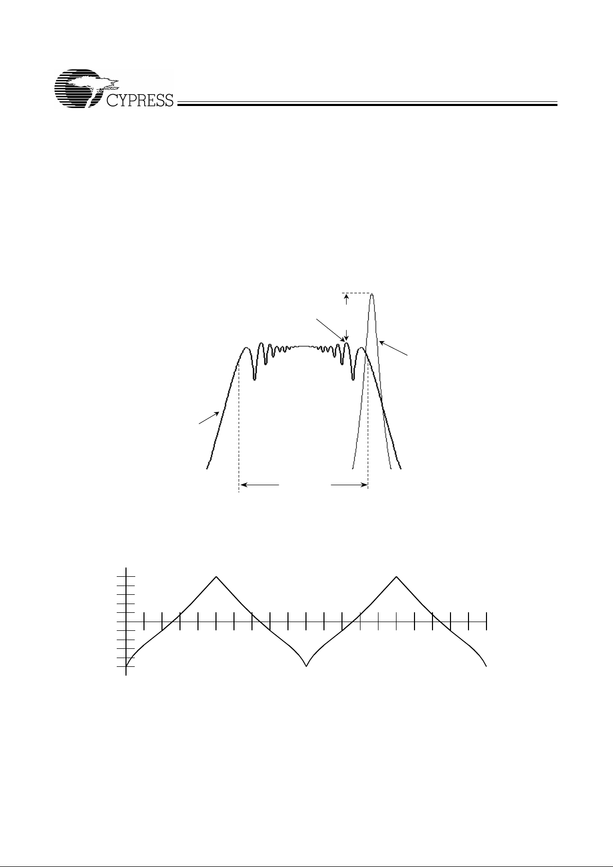
Spread Sp ectrum Clockin g
The device generates a clock that is frequency modulated in
order to increase the bandwidth that it occu pies. By increas ing
the bandwidth of the fundamental and its harmonics, the amplitudes of the radiated electromagnetic emissions are reduced. This effect is depicted in Figure 1.
As shown in Figure 1, a harmonic of a modulated clock has a
much low er amplitude th an that of an un modulated si gnal. The
reduction in amplitude is dependent on the harmonic number
and the frequency deviation or spread. The equation for the
reduction is:
dB = 6.5 + 9*log
10
(P) + 9*log10(F)
Where P is the perce nta ge of de viati on and F is the frequen cy
in MHz where the reduction is measured.
The output clock is modulated with a waveform depicted in
Figure 2. This waveform, as discussed in “Spread Spectrum
Clock Generation f or the Reducti on of Radiated Emissio ns” by
Bush, Fessler, and Hardin produces the maximum reduction
in the amplitude of radiated electromagnetic emissions. The
deviation selected for this chip is –0.5%, –1.0%, or ±0.9% of
the selected frequency. Figure 2 detail s the Cypre ss spr eading
pattern. Cypress does offer options with more spread and
greater EMI r eduction. Cont act your local Sal es represe ntativ e
for details on these devices .
Spread Spectrum clocking is activated or deactivated by selecting the appropriate values for SPREAD#.
Figure 1. Clock Harmonic with and without SSCG Modulation Frequency Domain Representation
∆
SSC
non-SSC
Highest peak
δ of f
nom
f
nom
MAX (+0.5%)
MIN (–0.5%)
10%
20%
30%
40%
50%
60%
70%
80%
90%
100%
10%
20%
30%
40%
50%
60%
70%
80%
90%
100%
FREQUENCY
Figure 2. Typica l Modulation Profile
Page 4

W48C101-01
PRELIMINARY
4
Absolute Maximum Ratings
Stresses gre ater th an those list ed i n this tab le may cause permanent damage to the de vice. These represent a str ess ratin g
only. Operation of the device at these or any other conditions
above those specified in the operating sect ions of this spec if ication is not implied. Maximum conditions for extended periods may affect reliability.
Parameter Description Rating Unit
V
DD
, V
IN
V oltage on any pin with respect to GND –0.5 to +7.0 V
T
STG
Storage Temperature –65 to +150 °C
T
A
Operating Temperature 0 to +70 °C
T
B
Ambient Temperature under Bias –55 to +125 °C
ESD
PROT
Input ESD Protection 2 (min.) kV
DC Electr i cal C h ar acteristics :
TA = 0°C to +70°C, V
DDQ3
= 3.3V±5%, V
DDQ2
= 2.5V±5%
Parameter Description T est Condi tion Min. Typ. Max. Unit
Supply Current
I
DDQ3
3.3V Supply Current CPU0:3 = 100 MHz
Outputs Loaded
[1]
120 mA
I
DDQ2
2.5V Supply Current CPU0:3 = 100 MHz
Outputs Loaded
[1]
65 mA
Logic Inputs
V
IL
Input Low Voltage GND – 0.3 0.8 V
V
IH
Input High Voltage 2.0 VDD + 0.3 V
I
IL
Input Low Current
[2]
–25 µA
I
IH
Input High Current
[2]
10 µA
I
IL
Input Low Current (SEL10 0/66#) –5µA
I
IH
Input High Current (SEL100/66#) 5 µA
Clock Outputs
V
OL
Output Low Voltage IOL = 1 mA 50 mV
V
OH
Output High Voltage IOH = –1 mA 3.1 V
V
OH
Output High Voltage CPU0:3 , APIC0 :1 IOH = –1 mA 2.2 V
I
OL
Output Low Current CPU0:3 V
OL
= 1.25V 45 65 100 mA
PCI_F, PCI1:7 V
OL
= 1.5V 70 100 145 mA
APIC0:1 V
OL
= 1.25V 60 90 140 mA
REF0:2 V
OL
= 1.5V 45 65 100 mA
48MHz V
OL
= 1.5V 45 65 100 mA
I
OH
Output High Current CPU0:3 V
OL
= 1.25V 45 65 100 mA
PCI_F, PCI1:7 V
OL
= 1.5V 65 95 135 mA
APIC0:1 V
OL
= 1.25V 55 80 115 mA
REF0:2 V
OL
= 1.5V 45 65 100 mA
48MHz V
OL
= 1.5V 45 65 100 mA
Notes:
1. All clock outputs loaded with 6" 60Ω transmission lines with 20-pF capacitors.
2. W48C101-01 logic inputs have internal pull-up devices, except SEL100/66# (pull-ups not full CMOS level).
Page 5

W48C101-01
PRELIMINARY
5
AC Electrical Characteristics
T
A
= 0°C to +70°C, V
DDQ3
= 3.3V±5%,V
DDQ2
= 2.5V± 5%, f
XTL
= 14.31818 MHz
AC clock parameters are tested and guaranteed over stated operating conditions using the stated lump capacitive load at the
clock output; Spread Spectrum clocking is disabled.
Crystal Oscillator
V
TH
X1 Input Threshold Voltage
[3]
1.65 V
C
LOAD
Load Capacitanc e, as seen by External Crystal
[4]
14 pF
C
IN,X1
X1 Input Capacitance
[5]
Pin X2 unconnected 28 pF
Pin Capacitance/Induct ance
C
IN
Input Pin Capacitanc e Except X1 and X2 5 pF
C
OUT
Output Pin Capacitance 6pF
L
IN
Input Pin Inductance 7nH
Notes:
3. X1 input threshold voltage (typical) is V
DD
/2.
4. The W48C101-01 contains an internal crystal load capacitor between pin X1 and ground and another between pin X2 and ground. Total load placed on crystal
is 14 pF; this includes typical stray capacitance of short PCB traces to crystal.
5. X1 input capacitance is applicable when driving X1 with an external clock source (X2 is left unconnected).
DC Electr i cal C h ar acteristics :
TA = 0°C to +70°C, V
DDQ3
= 3.3V±5%, V
DDQ2
= 2.5V±5% (continued)
Parameter Description T est Condi tion Min. Typ. Max. Unit
CPU Clock Outputs, CPU0:3 (Lump Capacitance Test Load = 20 pF)
Parameter Description Test Condition/ Comment s
CPU = 66.6 MHz CPU = 100 MHz
UnitMin. Typ. Max. Min. Typ. Max.
t
P
Period Measured on rising edge at 1.25V 15 15.5 10 10.5 ns
t
H
High Time Duration of clock cycle above 2.0V 5.2 3.0 ns
t
L
Low Time Duration of clock cycle below 0.4V 5.0 2.8 ns
t
R
Output Rise Edge Rate Me asured from 0.4V to 2.0V 1 4 1 4 V/ns
t
F
Output Fall Edge Rate Measured from 2.0V to 0.4V 1 4 1 4 V/ns
t
D
Duty Cycle Measured on rising and falling edge at
1.25V
45 55 45 55 %
t
JC
Jitter , Cycle-to-Cycle Measured on rising edge at 1.25V. Max-
imum differ ence of cycle time between
two adjacent cycles.
200 200 ps
t
SK
Output Skew Measured on rising edge at 1.25V 175 175 ps
f
ST
Frequency Stabilization from Po wer-up
(cold start)
Assumes full supply voltage reached
within 1 ms from power-up . Short cycles
exist prior to frequency stabilization.
33ms
Z
o
AC Output Impedance Average value during switching transi-
tion. Used for dete rmini ng series terminat i o n value.
20 20 Ω
Page 6

W48C101-01
PRELIMINARY
6
PCI Clock Outputs, PCI1:7 and PCI_F (L ump Capacitance Test Load = 30 pF
Parameter Description Te st Condi tion/Comments
CPU = 66.6/100 MHz
UnitMin. Typ. Max.
t
P
Period Measured on rising edge at 1.5V 3 0 ns
t
H
High Time Duration of cloc k cycle above 2.4V 12 ns
t
L
Low Time Duration of clock cycle below 0.4V 12 ns
t
R
Output Rise Edge Rate Measured from 0.4V to 2.4V 1 4 V/ns
t
F
Output Fall Edge Rate Measured from 2.4V to 0.4V 1 4 V/ns
t
D
Duty Cycle Measured on rising and falling edge at 1.5V 45 55 %
t
JC
Jitter , Cycle-to-Cycle Measured on rising edge at 1.5V. Maximum
differ ence of cyc le time be tween tw o adjacent cycles .
250 ps
t
SK
Output Skew Measured on rising edge at 1.5V 500 ps
t
O
CPU to PCI Clock Skew Covers all CPU/PCI outputs. Measured on rising
edge at 1.5V. CPU leads PCI output.
1.5 4 ns
f
ST
Frequency Stabilization
from Power-up (cold
start)
Assumes full supply voltage reached within 1 ms
from power-up. Short cycles exist prior to frequency
stabilization.
3ms
Z
o
AC Output Impeda nce Average value duri ng switching transition. Used for
determining series termination value.
15 Ω
APIC0:1 Clock Outputs (Lump Capacitance Test Load = 20 pF)
Parameter Description Test Condition/Comments
CPU = 66.6/100MHz
UnitMin. Typ. Max.
f Frequency, Actual Frequency generated by crystal oscillator 14.31818 MHz
t
R
Output Rise Edge Rate Measured from 0.4V to 2.0V 1 4 V/ns
t
F
Output Fall Edge Rate Measured from 2.0V to 0.4V 1 4 V/ns
t
D
Duty Cycle Measured on rising and falling edge at 1.25V 45 55 %
f
ST
Frequency Stabilization
from Power-up (cold start)
Assumes full supply voltage reached within
1 ms from power-up . Short cycles e xist prior t o
frequency stabilization.
1.5 ms
Z
o
AC Output Impedance Av erage value during s witching transit ion.
Used for dete rmining series terminati on value .
15 Ω
REF0:2 Clock Outputs (Lump Capacitance Test Load = 20 pF)
Parameter Description Test Condition/Comments
CPU = 66.6/100 MHz
UnitMin. Typ. Max.
f Frequency, Actual Frequency generated by crystal oscillator 14.318 MHz
t
R
Output Rise Edge Rate Measured from 0.4V to 2.4V 0.5 2 V/ns
t
F
Output Fal l Edge Rate Measured fr om 2.4V t o 0.4V 0.5 2 V/ns
t
D
Duty Cycle Measured on rising and falling edge at 1.5V 45 55 %
f
ST
Frequency St abilization from
Power-up (cold start)
Assumes full supply voltage reached within 1 ms
from power-up. Short cycles exist prior to
frequency stabi li zation.
3ms
Z
o
AC Output Impedance A verage val ue during switching tra nsition. Used for
determining series termination value.
25 Ω
Page 7

W48C101-01
PRELIMINARY
7
Document #: 38-00852
48-MHz Clock Outputs (Lump Capacitance Test Load = 20 pF = 66.6/100 MHz)
Parameter Description Test Condition/Comments
CPU = 66.6/100 MHz
UnitMin. Typ. Max.
f Frequency, Actual Determined by PLL divider ratio (see m/n bel ow) 48.008 MHz
f
D
Deviation from 48 MHz (48.008 – 48)/48 +167 ppm
m/n PLL Ratio (14.31818 MHz x 57/17 = 48.008 MHz) 57/17
t
R
Output Rise Edge Rate Measured from 0.4V to 2.4V 1 4 V/ns
t
F
Output Fall Edge Rate Measured from 2.4V to 0.4V 1 4 V/ns
t
D
Duty Cycle Measured on rising and falling edge at 1.5V 45 55 %
f
ST
Frequency Stabilization
from Power-up (cold start)
Assumes full supply vol tage reached withi n 1 ms
from power-up. Short cycles exist prior to frequency stabilization.
3ms
Z
o
AC Output Impedance Average value during switching transition. Used
for determining seri es termi nation value.
25 Ω
Ordering Information
Ordering Code
Freq. Mask
Code
Package
Name Pack age Type
W48C101 -01 H 48-pin SSOP (300 mils)
Page 8

W48C101-01
PRELIMINARY
© Cypress Semiconductor Corporation, 1999. The information contained herein is subject to change without notice. Cypress Semiconductor Corporation assumes no responsibility for the use
of any circuitry other than circuitry embodied in a Cypress Semiconductor product. Nor does it con vey or imply any license under patent or other rights. Cypress Semiconductor does not authorize
its products for use as critical components in life-support systems where a malfunction or failure may reasonably be expected to result in significant injury to the user. The inclusion of Cypress
Semiconductor products in life-support systems application implies that the manufacturer assumes all risk of such use and in doing so indemnifies Cypress Semiconductor against all charges.
Package Diagram
48-Pin Small Shrink Outlin e P ackage (SSOP, 300 mils)
Summary of nominal dimensions in inches:
Body Width: 0.296
Lead Pitch: 0.025
Body Length: 0.625
Body Height: 0.102
 Loading...