

Page 1
W42C31-09
Spread Spectrum Frequency Timing Generator
Features
• Maximized EMI suppression usi ng Cypress’s Spread
Spec trum te chnol ogy
• Generates a spread spectrum copy of the provided
input
• Integrated loop filter components
• Operates with a 3.3V or 5V supply
• Low-power CMOS design
• Available in 8-pin SOIC (Small Outline Integrated
Circuit)
Overview
The W42C31-09 incorporates the latest advances in PLL
spread spectrum frequency synthesizer techniques. By frequency modulating the output with a low-frequency carrier,
EMI is greatly reduced. Use of this technology allows systems
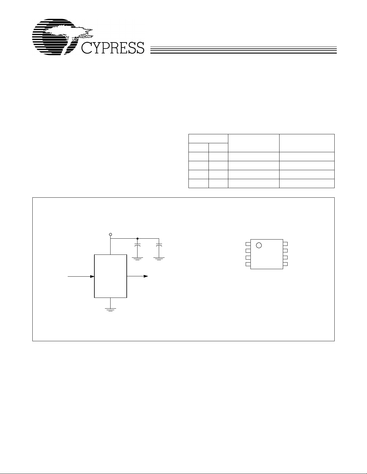
Simplified Block Diagram
VDD
Oscillator or Refer ence
Input
W42C31-09
(EMI suppressed)
Spread Spectrum
Output
to pass increasingly difficult EMI testing without resorting to
costly shiel ding or redesign.
In a system, not on ly is EMI reduced i n the v ari ous cl oc k lin es,
but also in all signals which are synchronized to the clock.
Therefore, the benefits of using this technology increase with
the number of address and data lines in the system. The Simplified Block Diagram shows a simple implementation.
T able 1. Frequency Spread Selection
W42C31-09
0 0 30 to 55 f
0 1 30 to 55 f
1 0 30 to 55 f
1 1 30 to 55 f
Input Frequency
(MHz)
Output Frequency
(MHz)FS1 FS0
±0.625%
IN
±1.25%
IN
±2.5%
IN
–3.75%
IN
Pin Configuration
SOIC
CLKIN
NC
GND
FS1
W42C31-09
1
2
3
4
8
7
6
5
SSON#
CLKOUT
FS0
VDD
Cypress Semiconductor Corporation
• 3901 North First Street • San Jose • CA 95134 • 408-943-2600
January 25, 2000, rev. *B
Page 2
Pin Definitions
W42C31-09
Pin Name Pin No.
CLKOUT 7 O
T ype Pin Description
Output Modulated Fr equency
clock.
Pin
CLKIN 1 I
NC 2 I
SSON# 8 I
External Reference Frequency Input
No Connect:
This pin must be left unconnected.
Spread Spectrum Control (Active LOW):
internal modulation wa veform on. This pin has an internal pull-down resi stor.
FS0:1 6, 4 I
Frequency Selection Bit 0:
characteristics. Refer to Table 1 . These pins have internal pull-up resistors.
VDD 5 P
GND 3 G
Power Connection:
Ground Connection:
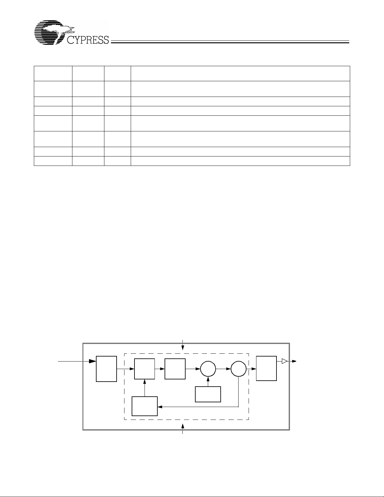
Functional Description
The W42C31-09 uses a p hase- loc k ed loop ( PLL) t o freq uency
modulate an input clock. The result is an output clock whose
frequency is slowly swept over a narrow band near the input
signal. The basic circuit topology is shown in Figure 1. The
input reference signal is divided by Q and fed to the phase
detector. A signal from the VCO is divided by P and fed back
to the phase detec tor al so . The PLL will f or ce the fr equency of
the VCO output sign al to change until the divid ed output signal
and the divided reference signal match at the phase detector
input. The output frequency is then equal to the ratio of P/Q
times the reference frequency. (Not e: For the W42C31-09 the
output frequency is equal to the input frequency.) The unique
feature of the Spread Spectrum Frequency Timing Generator
is that a modul ating waveform is s uperi m posed at the input to
the VCO. This causes the VCO output to be slowly swept
across a predetermined frequency band.
Because the modulating frequency is typically 1000 times
slower than the fundamental clock, the spread spectrum process has litt le i m pact on system performance.
: Fre quenc y modul ated cop y of the un modul ate d input
Pulling this input signal LOW turns the
These pins select the frequency spreading
Connected to 3.3V or 5V pow er supply.
This should be connect ed to the common ground plane.
Frequency Selection With SSFTG
In Spread Spectrum Frequency Timing Generation, EMI reduction depends on the shape, modulation percentage, and
frequency of the modulating waveform. While the shape and
frequency of the modulating waveform are fixed, the modulation percentage may be varied.
Using frequency select bits (FS1:0 pins), various spreading
percentages can be chosen (see Table 1 ).
A larger spreading per centage improves EMI reduction. However, large spread percentages may either exceed system
maximum frequ ency ra tings or lo wer the a v erag e fr equency t o
a point where performance is affected. For these reasons,
spreading percentages between ±0.5% and ±2.5% are most
common.
The W42C31 feat ures t he abil ity to sel ect from v arious spread
spectrum characteristics. Selections specific to the
W42C31-09 are shown in Table 1. Other spreading char acter-
istics are available (see separate data sheets) or can be created with a custom mask. Also, other devices in the W42C31
family offer frequency multiplication in addition to the spread
spectrum function. This will allow the use of less expensive
fundamental mode crystals.
VDD
Clock Input
Reference Input (EMI suppressed)
Freq. Phase
Q
Detector
Feedback
Divider
P
Charge
Pump
GND
Σ
Modulating
Waveform
PLL
VCO
Post
DividersDivider
CLKOUT
Figure 1. System Block Diagra m (Co ncept, not actual implementat ion)
2
Page 3
W42C31-09
Spread Spectrum Frequency Timing
Generation
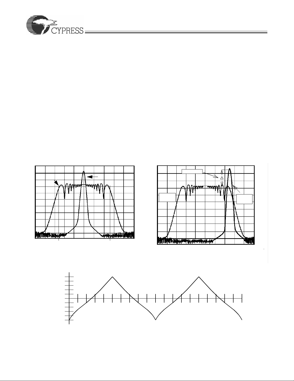
The benefits of using Spread Spectrum Frequency Timing
Generation are depicted in Figure 2. An EMI emission profile
of a clock harmonic is shown.
Contrast the typical clock EMI wi th the Cypress Spread Spectrum Frequency Timing Generation EMI. Notice the spike in
the typical clo c k. This sp ike can mak e system s f ail quas i-peak
EMI testing. The FCC and other regulatory agencies test for
peak emissions. With spr ead spectrum enabled, the peak energy is much lower (at least 8 dB) because the energy is
spread out across a wider ban dwidth.
Modulating Waveform
The shape of the modul ating wa vef orm is critica l to EMI reduction. The modulation scheme used to accomplish the maximum reduction in EMI is shown in Figure 3. The period of the
modulation is shown as a percentage of the period length
along the X axis. The amount that the frequency is varied is
shown along the Y axis, also shown as a percentage of the
total frequency spread.
5dB/div
SSFTG Typical Clock
Cypress frequency selection tables express the modulation
percentage in t wo w ays . The fir st method dis pla ys the sp read ing frequency band as a percent of the programmed average
output frequency, symmetric about the programmed average
frequency. This method is always shown usi ng th e expre ssion
f
Center ± XMOD
% in the frequency spr ead selection table.
The second approach is to specify the maximum operating
frequency and the spr eading band as a per centage of this frequency. The output signal is swept from the lower edge of the
band to the maximum frequency. The expression for this approach is f
Cypress has taken care to ensure that f
MAX – XMOD
%. Whenever this expression is used,
will never be ex-
MAX
ceeded. This is important in applications where the clock
drives component s with ti ght maxi mum clo c k speed speci fica tions.
SSON# Pin
An internal pull-down resistor defaults the chip into a spread
spectrum mode. The SSON# pin enables the spreading feature when set LOW. The SSON# pin disables the spreading
feature when set HIGH (V
EMI Reduction
DD
).
Spread
Spectrum
Enabled
Amplitude (dB)
Frequency Span (MHz)
-SS% +SS%
Non-
Sprea d
Spectrum
Figure 2. Typical Clock and SSFTG Comparison
100%
80%
60%
40%
20%
0%
–20%
–40%
Frequency Shift
–60%
–80%
–100%
10%
20%
30%
40%
50%
60%
70%
80%
90%
Time
100%
10%
20%
30%
40%
50%
60%
70%
80%
90%
100%
Figure 3. Modulation W aveform Prof il e
3
Page 4

Absolute Maximum Ratings
W42C31-09
Stresses gre ater th an those li sted i n this tab le may cause permanent damage to the de vice. These represent a stress ratin g
only. Operation of the device at these or any other conditions
above those specifie d in the operat ing sections of this specification is not implied. Maximum conditions for extended periods may affect reliability.
Parameter Description Rating Unit
V
, V
DD
IN
T
STG
T
A
T
B
P
D
DC Electr i cal C h ar acteristics:
Voltage on any pin with respect to GND –0.5 to +7 .0 V
Storage Temperature –65 to +150 °C
Operating Temperature 0 to +70 °C
Ambient Temperature under Bias –55 to +125 °C
Power Dissipation 0.5 W
0°C < T
< 70°C, VDD = 3.3V ±10%
A
Parameter Description Test Condition Min Typ Max Unit
I
t
DD
ON
Supply Current 18 32 mA
Power Up Time First locked clock cycle after
5ms
Power Good
V
(Logic Inputs) Input Low Voltage 0.8 V
IL
V
(CLKIN) Input Low Voltage .4 V
IL
(Logic Inputs) Inpu t Hig h Voltage 2.4 V
V
IH
V
(CLKIN) Input High Voltage 2.8 V
IH
V
OL
V
OH
I
IL
I
IH
I
OL
I
OH
C
I
C
I
R
P
Z
OUT
Notes:
1. Output driver is full CMOS.
2. Inputs FS1:0 have a pull-up resistor, Input SSON# has a pull-down resistor.
Output Low Voltage IOL = 21.6 mA
Output High Voltage I
= 31.5 mA
OH
Input Low Current Note 2 –100 µA
Input High Current Note 2 10 µA
Output Low Current @ 0.4V, VDD = 3.3V 15 mA
Output High Current @ 2.4V, VDD = 3.3V 15 mA
Input Capacitance All pins except CLKIN 7 pF
Input Capacitance CLKIN pin only 6 10 pF
Input Pull-Up Resistor 500 kΩ
Clock Output Impedance 25 Ω
[1]
[1]
2.5 V
0.4 V
4
Page 5

W42C31-09
DC Electr i cal C h ar acteristics:
0°C < T
< 70°C, VDD = 5V ±10%
A
Parameter Description Test Condition Min Typ Max Unit
I
DD
t
ON
V
(Logic Inputs) Input Low Voltage 0.15V
IL
(CLKIN) Input Low Voltage 0.4 V
V
IL
V
(Logic Inputs) Inpu t Hig h Voltage 0.7V
IH
(CLKIN) Input High Voltage 4.2 V
V
IH
V
OL
V
OH
I
IL
I
IH
I
OL
I
OH
C
I
C
I
R
P
Z
OUT
Supply Current 30 45 mA
Power Up Time First locked clock cycle after
5ms
Power Good
DD
DD
Output Low Voltage IOL = 25.7mA 0.4 V
Output High Voltage IOH = 118.mA 2.5 V
Input Low Current Note 2 –100 µA
Input High Current Note 2 10 µA
Output Low Current @ 0.4V, VDD = 5V 24 mA
Output High Current @ 2.4V, VDD = 5V 24 mA
Input Capacitance All pins except CLKIN 7 pF
Input Capacitance CLKIN pin only 6 10 pF
Input Pull-Up Resistor 500 kΩ
Clock Output Impedance 25 Ω
TA = 0°C to +70°C, VDD = 3.3V±10%
AC Electrical Characteristics:
Symbol Parameter Test Condition Min Typ M ax Unit
f
IN
f
OUT
t
R
t
F
t
OD
t
ID
t
JCYC
Input Frequency I nput Clock 30 40 55 MHz
Output Frequency Spread Off 30 40 55 MHz
Output Rise Time V, 15-pF load 0.8 – 2. 4 2 5 ns
Output Fall Time V, 15-pF load 2.4 – 0.8 2 5 ns
Output Duty Cycle 15-pF load 40 60 %
Input Duty Cycle 40 60 %
Jitter, Cycle- to - C yc le 250 300 ps
Harmonic Reduction f
= 40 MHz, third harmonic
out
measured, reference board,
8dB
15-pF load
V
V
TA = 0°C to +70°C, VDD = 5V±10%
AC Electrical Characteristics:
Symbol Parameter Test Condition Min Typ M ax Unit
f
IN
f
OUT
t
R
t
F
t
OD
t
ID
t
JCYC
Input Frequency I nput Clock 30 40 55 MHz
Output Frequency Spread Off 30 40 55 MHz
Output Rise Time V, 15-pF load 0.8 – 2. 4 2 5 ns
Output Fall Time V, 15-pF load 2.4 – 0.8 2 5 ns
Output Duty Cycle 15-pF load 40 60 %
Input Duty Cycle 40 60 %
Jitter, Cycle- to - C yc le 250 300 ps
Harmonic Reduction f
= 40 MHz, third harmonic
out
measured, reference board,
8dB
15-pF load
5
Page 6

W42C31-09
Application Information
Recommended Circuit Configuration
For optimum performance in system applications the power
supply decoupli ng scheme sho wn in Figure 4 should be used.
decoupling is important to both reduce phase jitter and
V
DD
EMI radiation. The 0.1-µF decoupling capacitor should be
placed as close to the V
pin as possible, otherwise the in-
DD
Reference Input
NC
GND
5V or 3.3V System Supply
W42C31-09
1
2
3
4
8
7
6
5
Figure 4. Recommended Circuit Configuration
creased trace indu ctance will negate its decou pling capabili ty.
The 10-µF decoupling capacitor shown should be a tantalum
type. For further EMI protection, the V
made via a ferrite bead, as shown.
connection can be
DD
Recommended Board Layout
Figure 5 shows a recommended 2-layer board layout.
Clock Output
R1
VDD
C1
µF
0.1
FB
FB
G
C1 =
C2 =
R1 =
=
C2
µF Tantalum
10
High frequency supply decoupling
capacitor (0.1-
Common supply low frequency
decoupling capacitor (10recommended).
Match value to line impedance
Ferrite Bead
=
Via To GND Plane
µF recommended).
µF tantalu m
Refere nce Input
NC
G
R1
C1
G
C2
Power Supply Input
(3.3V or 5V)
FB
G
Figure 5. Recommended Board Layout (2-La yer Board)
Ordering Information
Freq. Mask
Ordering Code
Code
W42C31 09 G 8-pin Plastic SO IC (150-mil)
Document #: 38-00799-B
Package
Name
Package Type
6
Clock Output
Page 7

Package Diagram
W42C31-09
8-Pin Small Outline Integrated Circuit (SOI C, 150- m il )
© Cypress Semiconductor Corporation, 2000. The information contained herein is subject to change without notice. Cypress Semiconductor Corporation assumes no responsibility for the use
of any circuitry other than circuitry embodied in a Cypress Semiconductor product. Nor does it con vey or imply any lice nse under patent or other rights. Cypress Semicondu ctor does not authorize
its products for use as critical components in life-support systems where a malfunction or failure may reasonably be expected to result in significant injury to the user. The inclusion of Cypress
Semiconductor products in life-support systems application implies that the manufacturer assumes all risk of such use and in doing so indemnifies Cypress Semiconductor against all charges.
 Loading...