

Page 1
W40S11-02
SDRAM Buffer - 2 DIMM (Mobile)
Features
• Ten skew-controlled CMOS outputs (SDRAM0:9)
• Supports two SDRAM DIMMs
• Ideal for hi gh-performance systems designed around
Intel®’s latest Mobile chip set
2
•I
C Serial configuration interface
• Skew between any two outputs is less than 250 ps
• 1 to 5 ns propagatio n delay
• DC to 133-MHz operation
• Single 3.3V supply voltage
• Low power CMOS design pa ckaged i n a 28-pi n, 209-mil
SSOP (Shrink Small Outline Package)
Overview
The Cypress W40S11-02 is a low-voltage, ten-output clock
buffer. Output buffer impedance is approximately 15Ω, which
is ideal for driving SDRAM DIMMs.
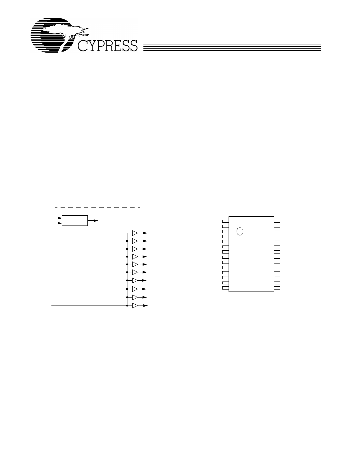
Block Diagram
SDATA
SCLOCK
BUF_IN
Serial Port
Device Control
OE
SDRAM0
SDRAM1
SDRAM2
SDRAM3
SDRAM4
SDRAM5
SDRAM6
SDRAM7
SDRAM8
SDRAM9
Key Specifications
Supply Voltages:...........................................VDD = 3.3V±5%
Operating Tempe ra tu re : .................................... 0° C to +70°C
Input Threshold: ..................................................1.5V typical
Maximu m In p ut Voltage:............. ..........................V
DD
+ 0.5V
Input Frequency:...............................................0 to 133 MHz
BUF_IN to SDRAM0:9 Propagation Delay:........1.0 to 5.0 ns
Output Edge Rate:....................... .. .. ............. .. ....... >
1.5 V/ns
Output Skew:............................................................ ±250 ps
Output Duty Cyc le : .... .. ............................ 45/5 5 % worst case
Output Impedance:...................... .. ................15 ohms typical
Output Ty pe:................................................ CMOS rail-to-rail
Pin Configuration
VDD
SDRAM0
SDRAM1
GND
VDD
SDRAM2
SDRAM3
GND
BUF_IN
VDD
SDRAM8
GND
VDD
SDATA
Note:
1. Internal pull-up resistor of 250K on SDATA, SCLOCK, and OE
inputs (should not be relied upon for pulling up to V
1
2
3
4
5
6
7
8
9
10
11
12
13
[1]
14
28
27
26
25
24
23
22
21
20
19
18
17
16
15
VDD
SDRAM7
SDRAM6
GND
VDD
SDRAM5
SDRAM4
GND
[1]
OE
VDD
SDRAM9
GND
GND
SCLOCK
DD
[1]
).
Intel is a registered trademark of Intel Corporation.
Cypress Semiconductor Corporation
• 3901 North First Street • San Jose • CA 95134 • 408-943-2600
September 29, 1999, r ev. **
Page 2
Pin Definitions
W40S11-02
Pin Name
No.
SDRAM0:9 2, 3, 6, 7,
Pin
Pin
Type Pin Description
O
22, 23, 26,
27, 11, 18
BUF_IN 9 I
SDATA 14 I/O
SCLOCK 15 I
VDD 1, 5, 10, 13,
P
19, 24, 28
GND 4, 8, 12, 16,
G
17, 21, 25
OE 20 I
SDRAM Outputs:
Provides buffered copy of BUF_IN. The propagation delay from a
rising input edge to a rising outp ut edge is 1 to 5 ns. All outputs are skew controlled
to within ± 250 ps of each other.
Clock Input:
2
C Data Input:
I
This clock inpu t has an i nput threshold voltage of 1.5V (typ).
Data should be pr esented to t his inpu t as described i n the I
2
C section
of this data sheet. Internal 250-kΩ pull-up resistor.
2
C Clock Input:
I
2
in the I
C section of this data sheet . Internal 250-kΩ pull-up resistor.
Power Connection:
2
The I
C Data clock should be presented to this input as described
Power supply for cor e logi c and output buff ers. Connected to
3.3V supply.
Ground Connection:
Output Enable:
Connect all g round pins to the common syst em ground plane.
Internal 250-kΩ pull-up resistor. Three-states out puts when LOW.
2
Page 3
W40S11-02
Functional Description
Output Control Pins
Outputs three-stated when OE = 0, and toggle when OE = 1.
Outputs are in phase wit h BUF_IN b ut are pha se del a yed by 1
to 5 ns. Outputs can also be controlled via the I
Table 1. Byte Writing Sequence
Byte
Sequence Byte Name Bit Sequence Byte Description
1 Slave Address 11010010 Commands the W40S11-02 to acce pt the bits in Data Bytes 0–6 for in-
2 Command
Code
3 Byte Count Don’t Care Unused by the W40S1 1-02 , ther ef or e bit val ues ar e i gnored (don ’t care ).
4 Data Byte 0 Refer to Table 2 The data bit s in thes e bytes set int ernal W40S11-23 r egister s that co ntrol
5 Data Byte 1
6 Data Byte 2
7 Data Byte 3 Don’t Care Refer to Cypress clock drivers.
8 Data Byte 4
9 Data Byte 5
10 Data Byte 6
Don’t Care Unused by the W40S1 1-02 , ther ef ore bi t val ues ar e igno red (don’t care).
2
C interfac e.
ternal register configuration. Since other devices ma y exist on the same
common serial data b us , it is neces sary to ha v e a sp ecific sl a ve a ddre ss
for each potential receiver . The sla ve re ceiver add ress for the W40S11-02
is 11010010. Register setting wil l not be made if the Slave Addr ess is not
correct (or is for an alternate slave receiver).
This byte must be included i n the data write sequen ce to maintain prop er
byte allocation. The Command Code Byte is part of the standard serial
communication protocol and may be used when writing to another addressed slave receiver on the serial data bus.
This byte must be included i n the data write sequen ce to maintain prop er
byte allocation. The Byte Count Byte is part of the standard serial communication pr otocol and may be used when writ ing to another address ed
slave receiver on the serial data bus.
device oper ation. The data bits are only accepted when the Address Byte
bit sequence i s 11010010, as noted above. For descri pti on of bit control
functions, refer to Table 2, Data Byte Serial Configuration Map.
Output Drivers
The W40S11-02 output buffers are CMOS type which deliver
a rail-to-rail (GND to V
capacitiv e load . Thus , o utput s ignal ing is both TTL and CMOS
level compatible. Nomina l output buffer imped ance is 15 ohms.
Operation
Data is written to the W40S11-02 in ten bytes of eight bits
each. Bytes are written in the order shown in Table 1.
) output voltage sw ing into a nominal
DD
3
Page 4
W40S11-02
Writing Data Bytes
Each bit in the data bytes control a particular device function.
Table 2 gives the bit f ormats fo r registers lo cated in Data Byt es
0–6.
Bits are written MSB (most significant bit) first, which is bit 7.
Table 2. Data Bytes 0–2 Seri al Configuration Map
Affected Pin
Bit(s)
Pin No. Pin Name 0 1
[2]
Control Function
Bit Control
Data Byte 0 SDRAM Active/Inactive Register (1=Enable, 0=Disable)
7 N/A Reserved (Reserved) -- -6 N/A Reserved (Reserved) -- -5 N/A Reserved (Reserved) -- -4 N/A Reserved (Reserved) -- -3 7 SDRAM3 Clock Output Disable Low Active
2 6 SDRAM2 Clock Output Disable Low Active
1 3 SDRAM1 Clock Output Disable Low Active
0 2 SDRAM0 Clock Output Disable Low Active
Data Byte 1 SDRAM Active/Inactive Register (1=Enable, 0=Disable)
7 27 SDRAM7 Clock Output Disable Low Active
6 26 SDRAM6 Clock Output Disable Low Active
5 23 SDRAM5 Clock Output Disable Low Active
4 22 SDRAM4 Clock Output Disable Low Active
3 N/A Reserved (Reserved) -- -2 N/A Reserved (Reserved) -- -1 N/A Reserved (Reserved) -- -0 N/A Reserved (Reserved) -- --
Data Byte 2 SDRAM Active/Inactive Register (1=Enable, 0=Disable)
7 18 SDRAM9 Clock Output Disable Low Active
6 11 SDRAM8 Clock Output Disable Low Active
5 N/A Reserved (Reserved) -- -4 N/A Reserved (Reserved) -- -3 N/A Reserved (Reserved) -- -2 N/A Reserved (Reserved) -- -1 N/A Reserved (Reserved) -- -0 N/A Reserved (Reserved) -- --
Note:
2. At power-up all SDRAM outputs are enabled and active. It is recommended to program Bits 4–7 of Byte0 and Bits 0–3 of Byte1 to a “0” to save power and reduce
noise.
4
Page 5

W40S11-02
How To Use the Serial Data Interface
Electrical Requirements
Figure 1 illust rat es el ectrical ch aract eristi cs for the serial interface bus used with the W40S11-02. Devices send data over
the bus with an open drain l ogic output that can (a) pull the bus
line LOW, or (b) let t he b u s def au lt t o logi c 1. The pu ll- up resi stor on the bus (both clock and data lines) establish a default
SERIAL BUS DATA LINE
SERIAL BUS CLOCK LINE
SDCLK SDATA
N
DATA OUT
DATA IN
N
CLOCK IN
CLOCK OUT
logic 1. All bus devices generally have logic inputs to receive
data.
Although the W40S11-02 is a receive-only device (no data
write-back capability), it does transmit an “acknowledge” data
pulse after each byte is received. Thus, the SDATA line can
both transmit and receive data.
The pull-up resistor should be sized to meet the rise and fall
times specif ied i n A C p arame ters , ta king i nt o consi derat ion total bus line cap acitance.
VDD VDD
~ 2k
Ω
CLOCK IN
Ω
~ 2k
SCLOCK SDATA
DATA IN
DATA OUT
N
(SERIAL BUS MASTER TRANSMITTER)
CHIP SET
Figure 1. Serial Interface Bus Electrical Chara cteristics
(SERIAL BUS SLAVE RECEIVER)
CLOCK DEVICE
5
Page 6

W40S11-02
Sign aling R equi remen ts
As shown in Fi gure 2, v alid dat a bits ar e defined as stable logic
0 or 1 condition on the data line during a clock HIGH (logic 1)
pulse. A transi t ionin g data line duri ng a cloc k HIGH pulse may
be interpreted as a start or stop pulse (it will be interpreted as
a start or stop pulse if the start/stop timing parameters are
met).
A write sequence is i niti ated b y a “start bit ” as show n in Figure
3. A “stop bit” signifies that a transmission has ended.
As stated pre vi ously, the W40S11-0 2 s ends an “acknowledge”
pulse after receiving eight data bits in each byte as shown in
Figure 4.
SDATA
SCLOCK
Valid
Data
Bit
of Data Allowed
Sending Data to the W40S11-02
The device accepts data once it has detected a valid start bit
and address byte sequence. Device functionality is changed
upon the receipt of each dat a bit (regist ers are not doub le buff ered). Partial transmiss ion is allo wed meaning that a transm ission can be truncated as soon as the desired data bits are
transmitte d (remaining register s will be unmodifi ed). Transmission is truncated with either a stop bit or new start bit (restart
condition).
Change
SDATA
SCLOCK
Figure 2. Serial Data Bus Valid Data Bit
Start
Bit
Figure 3. Serial Data Bus Start and Stop Bit
Stop
Bit
6
Page 7

Figure 4. Serial Data Bus Write Sequence
Signaling from System Core Logic
Start Condition
MSB
11010010 LSB MSB MSB LSBSDATA
12345678A12345678A1234SCLOCK 12345678A
SDATA
Signaling by Clock Device
Slave Address
(First Byte)
LSB
MSB
Acknowledgment Bit
Command Code
(Second Byte)
from Clock Device
Byte Count
(Third Byte)
Last Data Byte
(Last Byte)
Stop Condition
7
Figure 5. Serial Data Bus Timing Diagram
SDATA
SCLOCK
t
STHD
t
LOW
t
t
DSU
t
HIGH
t
R
t
F
t
DHD
t
SP
t
SPSUtSTHD
t
SPSU
SPF
W40S11-02
Page 8

Absolute Maximum Ratings
W40S11-02
Stresses gre ater th an those li sted i n this tab le may cause permanent damage to the de vice. These represent a stress ratin g
only. Operation of the device at these or any other conditions
above those specified in the operating sections of this specif ication is not implied. Maximum conditions for extended periods may affect reliability.
Parameter Description Rating Unit
V
, V
DD
IN
T
STG
T
A
T
B
DC Electr i cal C h ar acteristi cs:
Voltage on any pin with respect to GND –0.5 to +7 .0 V
Storage Temperature –65 to +150 °C
Operating Temperature 0 to +70 °C
Ambient Temperature under Bias –55 to +125 °C
TA = 0°C to +70°C, VDD = 3.3V±5%
Parameter Description T est Condition/Comments Min T yp Max Unit
I
DD
I
DD
I
DD Tristate
3.3V Supply Current at 66 MHz 120 160 mA
3.3V Supply Current at 100 MHz 185 220 mA
3.3V Supply Current in
510mA
Three-State
Logic Inputs
V
IL
V
IH
I
ILEAK
I
ILEAK
Logic Outputs (SDRAM0:9)
V
OL
V
OH
I
OL
I
OH
Input Low Voltage VSS–0.3 0.8 V
Input High V oltage 2.0 VDD+0.5 V
Input Leakage Current, BUF_IN –5+5µA
Input Leakage Current
[4]
[3]
–20 +5 µA
Output Low Voltage IOL = 1 mA 50 mV
Output High Voltage IOH = –1 mA 3.1 V
Output Low Current VOL = 1.5V 70 110 185 mA
Output High Current VOH = 1.5V 65 100 160 mA
Pin Capacitance/Inductance
C
IN
C
OUT
L
IN
Note:
3. OE, SDATA, and SCLOCK logic pins have a 250-kΩ internal pull-up resistor (V
4. All SDRAM outputs loaded by 6" transmission lines with 22-pF capacitors on ends.
Input Pin Capacitance 5pF
Output Pin Capacitance 6 pF
Input Pin Inductance 7nH
– 0.8V).
DD
8
Page 9

W40S11-02
TA = 0°C to +70°C, VDD = 3.3V±5% (Lump Capacitance Test Load = 30 pF)
AC Electrical Characteristics:
Parameter Description Test Condition Min Typ Max Unit
f
t
t
t
t
t
t
t
t
t
Z
IN
R
F
SR
SF
EN
DIS
PR
PF
D
o
Input Frequency 0 133 MHz
Output Rise Edge Rate Measured f rom 0.4V to 2.4V 1.5 4.0 V/ns
Output Fall Edge Rate Measured from 2.4V to 0.4V 1.5 4.0 V/ns
Output Skew, Rising Edges 250 ps
Output Skew, Falling Edges 250 ps
Output Enable Time 1.0 8.0 ns
Output Disable Time 1.0 8.0 ns
Rising Edge Propagation Delay 1.0 5.0 ns
Falling Edge Propagation Delay 1.0 5.0 ns
Duty Cycle Measured at 1.5V 45 55 %
AC Output Impe dance 15 Ω
Ordering Information
Ordering Code
W40S11 -02 H
Freq. Mask
Code
Package
Name Package Type
X
28-pin SSOP (209-mil)
28-pin TSSOP (173-mil)
Document #: 38-00805
9
Page 10

Package Diagrams
W40S11-02
28-Pin Shrink Small Outlin e Package (TSSOP, 173-mil)
10
Page 11

W40S11-02
Package Diagrams
(continued)
28-Pin Small Shrink Outline Package (SSOP, 209 mils)
© Cypress Semiconductor Corporation, 1999. The information contained herein is subject to change without notice. Cypress Semiconductor Corporation assumes no responsibility for the use
of any circuitry other than circuitry embodied in a Cypress Semiconductor product. Nor does it con vey or imply any lice nse under patent or other rights. Cypress Semicondu ctor does not authorize
its products for use as critical components in life-support systems where a malfunction or failure may reasonably be expected to result in significant injury to the user. The inclusion of Cypress
Semiconductor products in life-support systems application implies that the manufacturer assumes all risk of such use and in doing so indemnifies Cypress Semiconductor against all charges.
 Loading...