

Datasheet W27E257P-15, W27E257P-12, W27E257P-10, W27E257-12, W27E257-10 Datasheet (Winbond Electronics)
Page 1
W27E257
BUFFER
CE
OE
32K × 8 ELECTRICALLY ERASABLE EPROM
GENERAL DESCRIPTION
The W27E257 is a high-speed, low-power Electrically Erasable and Programmable Read Only
Memory organized as 32768 × 8 bits that operates on a single 5 volt power supply. The W27E257
provides an electrical chip erase function. This part was the same EPROM Writer's utilities as the
W27E256.
FEATURES
• High speed access time:
100/120/150 nS (max.)
• Read operating current: 15 mA (typ.)
• Erase/Programming operating current
1 mA (typ.)
• Standby current: 5 µA (typ.)
• Single 5V power supply
• +14V erase/+12V programming voltage
• Fully static operation
• All inputs and outputs directly TTL/CMOS
compatible
• Three-state outputs
• Available packages: 28-pin 600 mil DIP and
32-pin PLCC
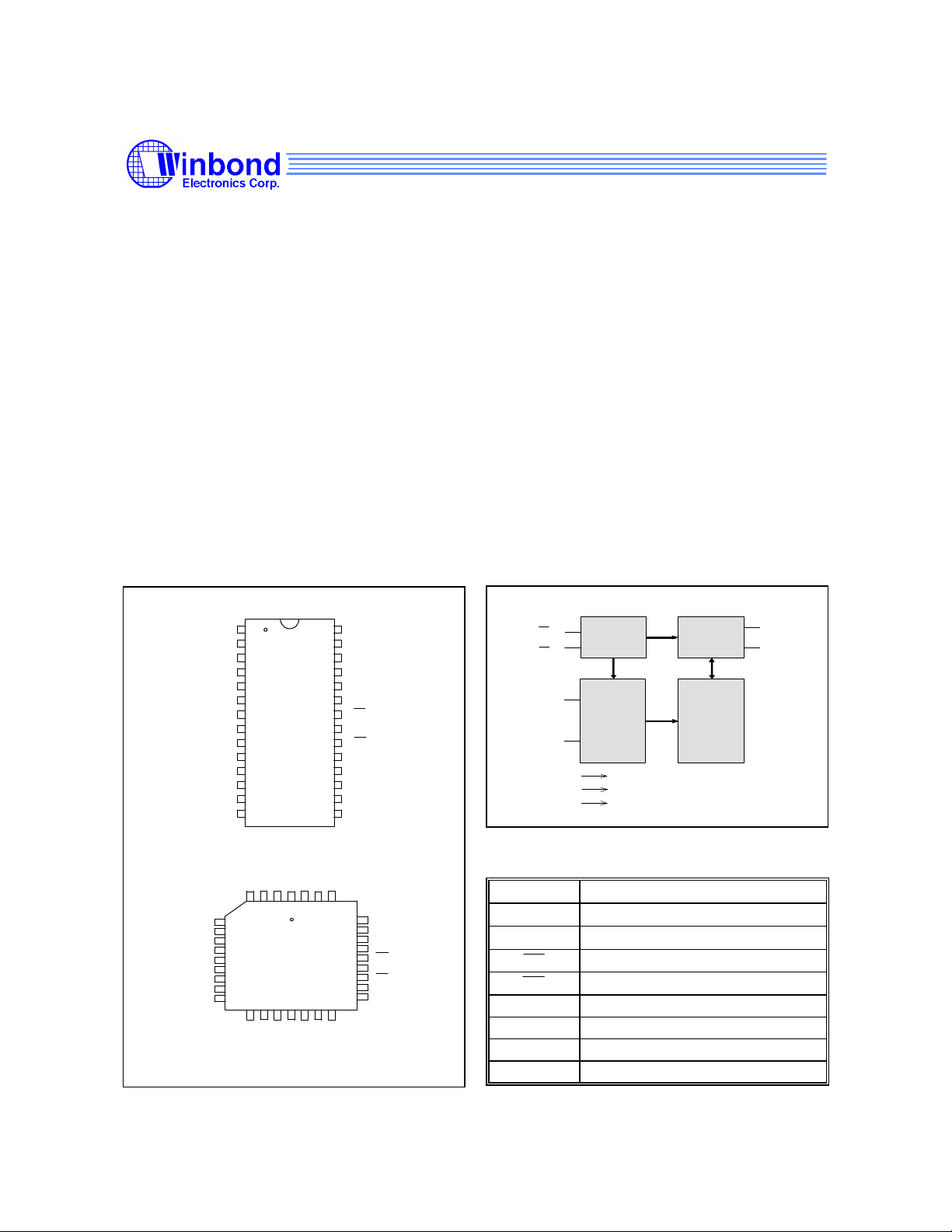
PIN CONFIGURATIONS
1
V
PP
2
A12
3
A7
4
A6
5
A5
6
A6
A5
A4
A3
A2
A1
A0
NC
Q0
A4
A3
A2
A1
A0
Q0
Q1
Q2
GND
5
6
7
8
9
10
11
12
1
13
4
28-pin
DIP
7
8
9
10
11
12
13
14
A
V
A
1
P
7
2
P
4 3 2 1
32-pin
151
6
Q
G
1Q2
N
D
N
C
PLCC
1
7
N
C
A
V
1
C
4
C
3
231
18192
Q3Q4Q
BLOCK DIAGRAM
V
28
CC
A14
27
A13
26
A8
25
A9
24
A11
23
22
OE
A10
21
20
CE
Q7
19
18
Q6
17
Q5
16
Q4
15
Q3
A
1
3
3
29
A8
0
A9
28
27
A11
NC
26
25
OE
A10
24
23
CE
22
Q7
21
Q6
0
5
PIN DESCRIPTION
A14
V
CC
GND
V
PP
CE
OE
A0
.
.
CONTROL
DECODER
OUTPUT
CORE
ARRAY
SYMBOL DESCRIPTION
A0−A14
Q0−Q7
Address Inputs
Data Inputs/Outputs
Chip Enable
Output Enable
VPP Program/Erase Supply Voltage
VCC Power Supply
GND Ground
NC No Connection
Q0
.
.
Q7
Publication Release Date: January 1997
- 1 - Revision A3
Page 2

W27E257
CE
CE
FUNCTIONAL DESCRIPTION
Read Mode
Like conventional UVEPROMs, the W27E257 has two control functions, both of which produce data
at the outputs.
is for power control and chip select. OE controls the output buffer to gate data to the output pins.
When addresses are stable, the address access time (TACC) is equal to the delay from CE to output
(TCE), and data are available at the outputs TOE after the falling edge of OE, if TACC and TCE timings
are met.
Erase Mode
The erase operation is the only way to change data from "0" to "1." Unlike conventional UVEPROMs,
which use ultraviolet light to erase the contents of the entire chip (a procedure that requires up to half
an hour), the W27E257 uses electrical erasure. Generally, the chip can be erased within 100 mS by
using an EPROM writer with a special erase algorithm.
Erase mode is entered when VPP is raised to VPE (14V), VCC = VCE (5V), OE = VIH (2V or above but
lower than VCC), A9 = VHH (14V), A0 = VIL (0.8V or below but higher than GND), and all other
address pins equal VIL and data input pins equal VIH. Pulsing CE low starts the erase operation.
Erase Verify Mode
After an erase operation, all of the bytes in the chip must be verified to check whether they have been
successfully erased to "1" or not. The erase verify mode automatically ensures a substantial erase
margin. This mode will be entered after the erase operation if VPP = VPE (14V), CE = VIH, and OE =
VIL.
Program Mode
Programming is performed exactly as it is in conventional UVEPROMs, and programming is the only
way to change cell data from "1" to "0." The program mode is entered when VPP is raised to VPP
(12V), VCC = VCP (5V), OE = VIH, the address pins equal the desired address, and the input pins
equal the desired inputs. Pulsing CE low starts the programming operation.
Program Verify Mode
All of the bytes in the chip must be verified to check whether or not they have been successfully
programmed with the desired data. Hence, after each byte is programmed, a program verify
operation should be performed. The program verify mode automatically ensures a substantial
program margin. This mode will be entered after the program operation if VPP = VPP (12V), CE = VIH,
and OE = VIL.
Erase/Program Inhibit
Erase or program inhibit mode allows parallel erasing or programming of multiple chips with different
data. When CE = VIH, erasing or programming of non-target chips is inhibited, so that except for the
and OE pins, the W27E257 may have common inputs.
- 2 -
Page 3
W27E257
Standby Mode
The standby mode significantly reduces VCC current. This mode is entered when CE = VIH. In
standby mode, all outputs are in a high impedance state, independent of OE.
Two-line Output Control
Since EPROMs are often used in large memory arrays, the W27E257 provides two control inputs for
multiple memory connections. Two-line control provides for lowest possible memory power
dissipation and ensures that data bus contention will not occur.
System Considerations
EPROM power switching characteristics require careful device decoupling. System designers are
interested in three supply current issues: standby current levels (ISB), active current levels (ICC), and
transient current peaks produced by the falling and rising edges of CE. Transient current magnitudes
depend on the device output's capacitive and inductive loading. Two-line control and proper
decoupling capacitor selection will suppress transient voltage peaks. Each device should have a 0.1 µ
F ceramic capacitor connected between its VCC and GND. This high frequency, low inherentinductance capacitor should be placed as close as possible to the device. Additionally, for every eight
devices, a 4.7 µF electrolytic capacitor should be placed at the array's power supply connection
between VCC and GND. The bulk capacitor will overcome voltage slumps caused by PC board trace
inductances.
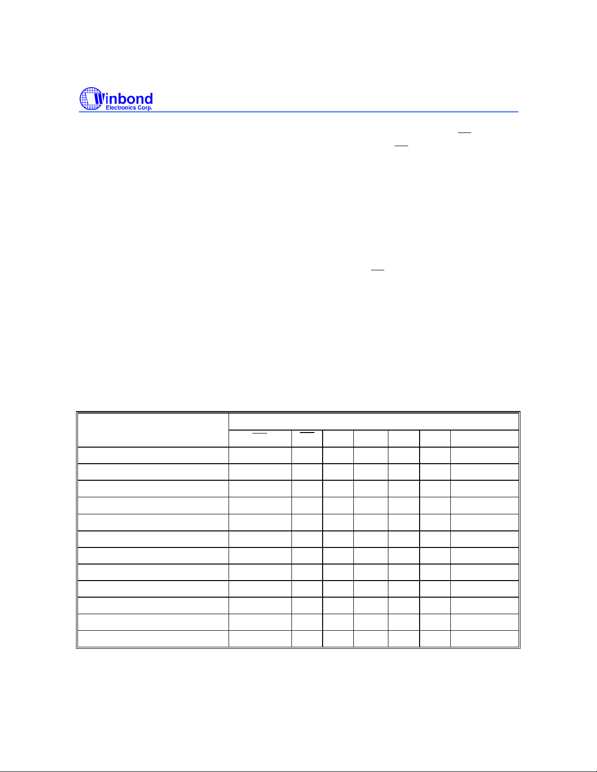
TABLE OF OPERATING MODES
(VPP = 12V, VPE = 14V, VHH = 12V, VCP = 5V, X = VIH or VIL)
MODE PINS
CE OE A0 A9 VCC VPP OUTPUTS
Read VIL VIL X X VCC VCC DOUT
Output Disable VIL VIH X X VCC VCC High Z
Standby (TTL) VIH X X X VCC VCC High Z
Standby (CMOS)
Program VIL VIH X X VCP VPP DIN
Program Verify VIH VIL X X VCP VPP DOUT
Program Inhibit VIH VIH X X VCP VPP High Z
Erase VIL VIH VIL VPE VCC VPE DIH
Erase Verify VIH VIL X X VCC VPE DOUT
Erase Inhibit VIH VIH X X VCP VPP High Z
Product Identifier-manufacturer VIL VIL VIL VHH VCC VCC DA (Hex)
Product Identifier-device VIL VIL VIH VHH VCC VCC 02 (Hex)
VCC ±0.3V
X X X VCC VCC High Z
Publication Release Date: January 1997
- 3 - Revision A3
Page 4
DC CHARACTERISTICS
CE
CE
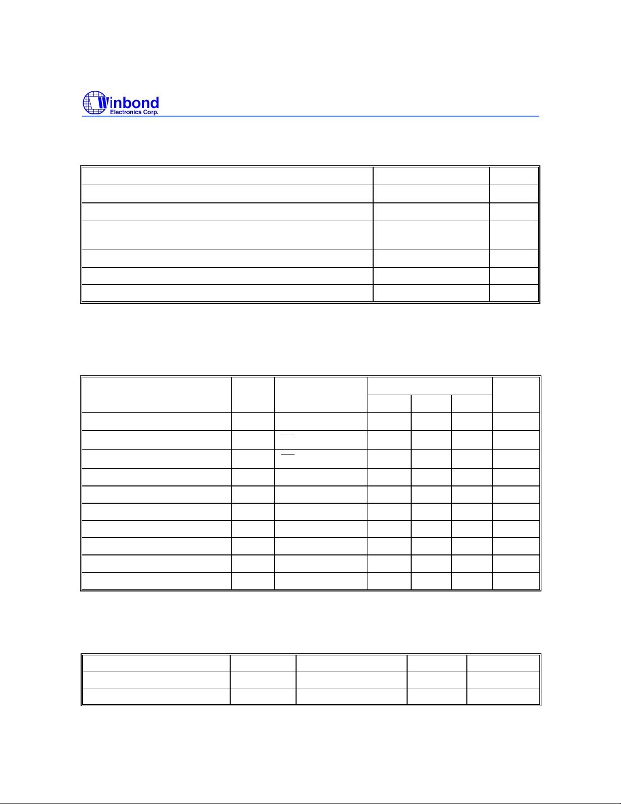
Absolute Maximum Ratings
PARAMETER RATING UNIT
W27E257
Ambient Temperature with Power Applied -55 to +125
Storage Temperature -65 to +125
Voltage on all pins with Respect to Ground Except VPP, A9
and VCC pins
Voltage on VPP Pin with Respect to Ground -0.5 to +14.5 V
Voltage on A9 Pin with Respect to Ground -0.5 to +14.5 V
Voltage on VCC Pin with Respect to Ground -0.5 to +7 V
Note: Exposure to conditions beyond those listed under Absolute Maximum Ratings may adversely affect the life and reliability of the
device.
-0.5 to VCC +0.5 V
°C
°C
DC Erase Characteristics
(TA = 25° C ±5° C, VCC = 5.0V ±10%)
PARAMETER SYM. CONDITIONS LIMITS UNIT
MIN. TYP. MAX.
Input Load Current ILI VIN = VIL or VIH -10 - 10
VCC Erase Current ICP
VPP Erase Current IPP
Input Low Voltage VIL - -0.3 - 0.8 V
= VIL
= VIL
- - 30 mA
- - 30 mA
µA
Input High Voltage VIH - 2.4 - 5.5 V
Output Low Voltage (Verify) VOL IOL = 2.1 mA - - 0.45 V
Output High Voltage (Verify) VOH IOH = -0.4 mA 2.4 - - A9 Erase Voltage VID - 13.75 14 14.25 V
VPP Erase Voltage VPE - 13.75 14 14.25 V
VCC Supply Voltage (Erase) VCE - 4.5 5.0 5.5 V
Note: VCC must be applied simultaneously or before VPP and removed simultaneously or after VPP.
CAPACITANCE
(VCC = 5V, TA = 25° C, f = 1 MHz)
PARAMETER SYMBOL CONDITIONS MAX. UNIT
Input Capacitance CIN VIN = 0V 6 pF
Output Capacitance COUT VOUT = 0V 12 pF
- 4 -
Page 5
W27E257
AC CHARACTERISTICS
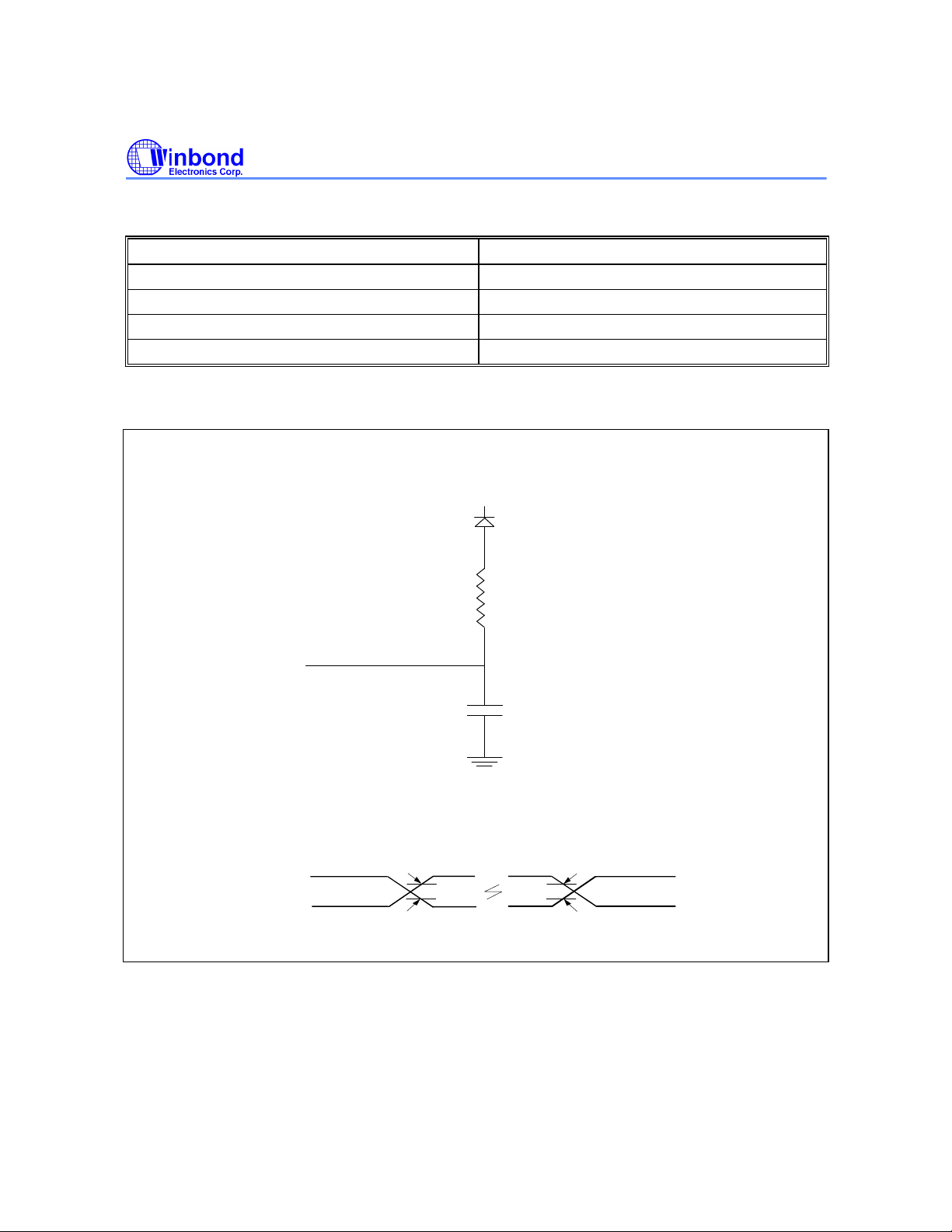
AC Test Conditions
PARAMETER CONDITIONS
Input Pulse Levels 0.45V to 2.4V
Input Rise and Fall Times 10 nS
Input and Output Timing Reference Level 0.8V/2.0V
Output Load CL = 100 pF, IOH/IOL = -0.4 mA/2.1 mA
AC Test Load and Waveform
+1.3V
(IN914)
D
OUT
Input
2.4V
0.45V
3.3K ohm
100 pF (Including Jig and Scope)
Output
Test Points Test Points
2.0V
0.8V
2.0V
0.8V
Publication Release Date: January 1997
- 5 - Revision A3
Page 6
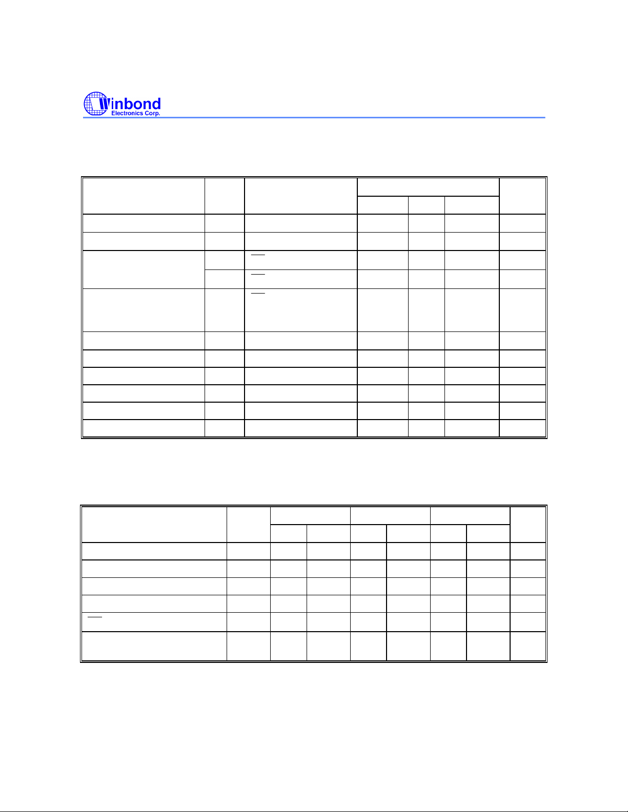
READ OPERATION DC CHARACTERISTICS
CE
CE
CE
OE
(VCC = 5.0V ±10%, TA = 0 to 70° C)
(W27E257-10, S-10, K-10, P-10: VCC, min. = 3.0V and max. = 5.5V)
PARAMETER SYM. CONDITIONS LIMITS UNIT
MIN. TYP. MAX.
W27E257
Input Load Current ILI VIN = 0V to VCC -5 - 5
Output Leakage Current ILO VOUT = 0V to VCC -10 - 10
VCC Standby Current ISB
ISB1
VCC Operating Current ICC
VPP Operating Current IPP VPP = VCC - - 100
Input Low Voltage VIL - -0.3 - 0.8 V
Input High Voltage VIH - 2.0 - VCC +0.5 V
Output Low Voltage VOL IOL = 2.1 mA - - 0.45 V
Output High Voltage VOH IOH = -0.4 mA 2.4 - - V
VPP Operating Voltage VPP - VCC -0.7 - VCC V
= VIH
= VCC ±0.2V
= VIL
IOUT = 0 mA
f = 5 MHz
- - 1.0 mA
- 5 100
- - 30 mA
READ OPERATION AC CHARACTERISTICS
(VCC = 5.0V ±10%, TA = 0 to 70° C)
PARAMETER SYM. W27E257-10 W27E257-12 W27E257-15 UNIT
µA
µA
µA
µA
MIN. MAX. MIN. MAX. MIN. MAX.
Read Cycle Time TRC 100 - 120 - 150 - nS
Chip Enable Access Time TCE - 100 - 120 - 150 nS
Address Access Time TACC - 100 - 120 - 150 nS
Output Enable Access Time TOE - 50 - 60 - 70 nS
High to High-Z Output
Output Hold from Address
Change
Note: VCC must be applied simultaneously or before VPP and removed simultaneously or after VPP.
TDF - 30 - 30 - 50 nS
TOH 0 - 0 - 0 - nS
- 6 -
Page 7
W27E257
CE
CE
CE
CE
OE
OE
OE
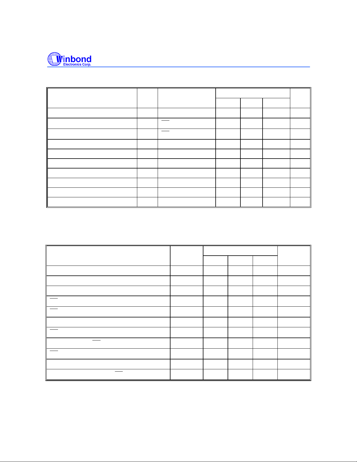
DC PROGRAMMING CHARACTERISTICS
(VCC = 5.0V ±10%, TA = 25° C ±5° C)
PARAMETER SYM. CONDITIONS LIMITS UNIT
MIN. TYP. MAX.
Input Load Current ILI VIN = VIL or VIH -10 - 10
VCC Program Current ICP
VPP Program Current IPP
Input Low Voltage VIL - -0.3 - 0.8 V
Input High Voltage VIH - 2.4 - 5.5 V
Output Low Voltage (Verify) VOL IOL = 2.1 mA - - 0.45 V
Output High Voltage (Verify) VOH IOH = -0.4 mA 2.4 - - V
A9 Silicon I.D. Voltage VID - 11.5 12.0 12.5 V
VPP Program Voltage VPP - 11.75 12.0 12.25 V
VCC Supply Voltage (Program) VCP - 4.5 5.0 5.5 V
= VIL
= VIL
- - 30 mA
- - 30 mA
µA
AC PROGRAMMING/ERASE CHARACTERISTICS
(VCC = 5.0V ±10%, TA = 25° C ±5° C)
PARAMETER SYM. LIMITS UNIT
MIN. TYP. MAX.
VPP Setup Time TVPS 2.0 - Address Setup Time TAS 2.0 - Data Setup Time TDS 2.0 - -
Program Pulse Width
Erase Pulse Width
Data Hold Time TDH 2.0 - -
Setup Time
Data Valid from
High to Output High Z
Address Hold Time TAH 0 - Address Hold Time after CE High (Erase)
Note: VCC must be applied simultaneously or before VPP and removed simultaneously or after VPP.
TPWP 95 100 105
TPWE 95 100 105 mS
TOES 2.0 - TOEV - - 150 nS
TDFP 0 - 130 nS
TAHC 2.0 - -
µS
µS
µS
µS
µS
µS
µS
µS
Publication Release Date: January 1997
- 7 - Revision A3
Page 8
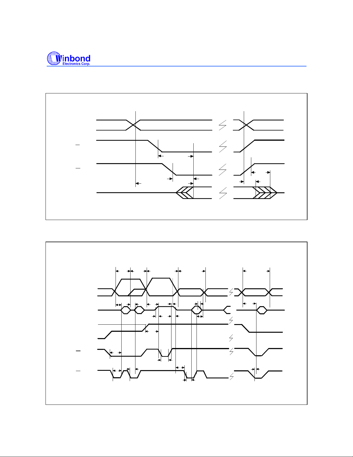
TIMING WAVEFORMS
Address Valid
IL
AC Read Waveform
V
IH
Address
V
IL
V
IH
CE
IL
IH
OE
V
IL
Outputs
High Z
W27E257
CE
T
T
DF
T
T
ACC
OE
Valid Output
T
OH
High Z
Erase Waveform
V
Data
V
OE
IH
V
IL
14.0V
5.0V
PP
V
IH
CE
V
IL
V
IH
V
IL
Address
Read
SID
A9 = 12.0V
A0= V
IL
Read
Device
SID
IH
IL
Others = V
T
ACC
IL
Manufacturer
Others = V
A0 = V
T
ACC
DA 02 Data All One
T
CE
T
T
OE
OE
Chip Erase
A9 = 14.0V
Others = V
T
AS
T
DS
T
VPS
T
T
ARC
PWE
Erase Verify
Address
Stable
T
AHC
T
OES
Blank Check
Read Verify
Address
Stable
T
DFP
D
OUT
T
AH
D
OUT
Address
Stable
T
ACC
D
OUT
5V
T
OE
T
OEV
- 8 -
Page 9
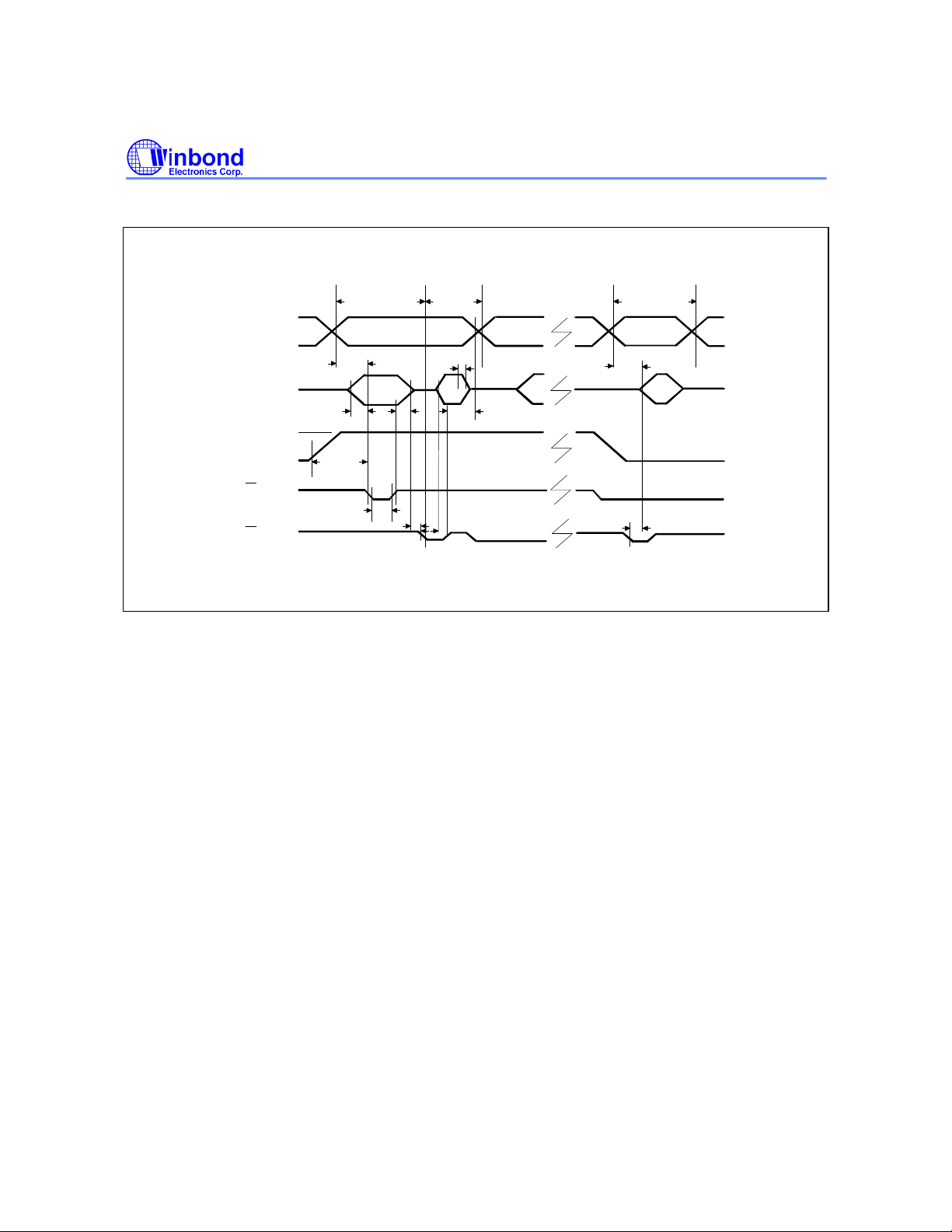
Timing Waveforms, continued
Programming Waveform
W27E257
Address
Data
V
Program
V
IH
V
IL
12.0V
PP
5.0V
V
IH
CE
V
IL
V
IH
OE
V
IL
T
T
VPS
Address Stable
AS
Data In Stable
T
DS
T
PWP
Program
Verify
Address Stable
T
DFP
D
OUT
T
DH
T
OES
T
AH
T
OEV
D
OUT
Read
Verify
Address Valid
T
ACC
T
OE
D
OUT
5V
Publication Release Date: January 1997
- 9 - Revision A3
Page 10
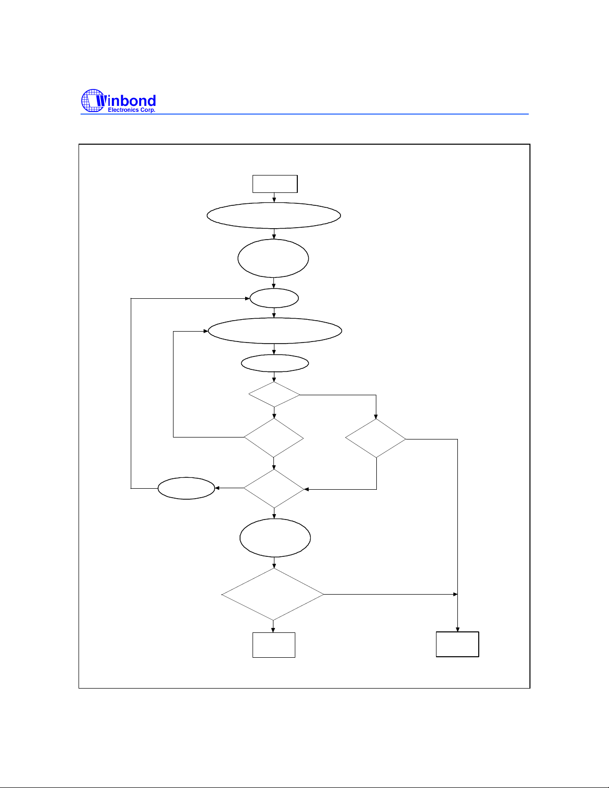
SMART PROGRAMMING ALGORITHM
Start
Address = First Location
Vcc = 5V
Vpp = 12V
X = 0
W27E257
Increment
Address
Program One 100 S Pulse
Increment X
X = 25?
Fail
No
Verify
One Byte
Last
Address?
Vcc = 5V
Vpp = 5V
Compare
All Bytes to
Original Data
µ
Yes
No
Pass
Yes
Fail
Verify
One Byte
Pass
Fail
Pass
Device
Pass
Fail
Device
- 10 -
Page 11
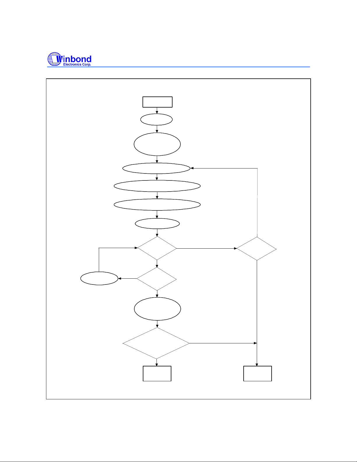
SMART ERASE ALGORITHM
W27E257
Start
X = 0
Vcc = 5V
Vpp = 14V
Increment
Address
A9 = 14V; A0 = V
Chip Erase 100 mS Pulse
Address = First Location
Increment X
Erase
Verify
No
Last
Address?
Vcc = 5V
Vpp = 5V
IL
Pass
Yes
No
Fail
X = 20?
Yes
Compare
All Bytes to
FFs (HEX)
Pass
Pass
Device
Fail
Fail
Device
Publication Release Date: January 1997
- 11 - Revision A3
Page 12
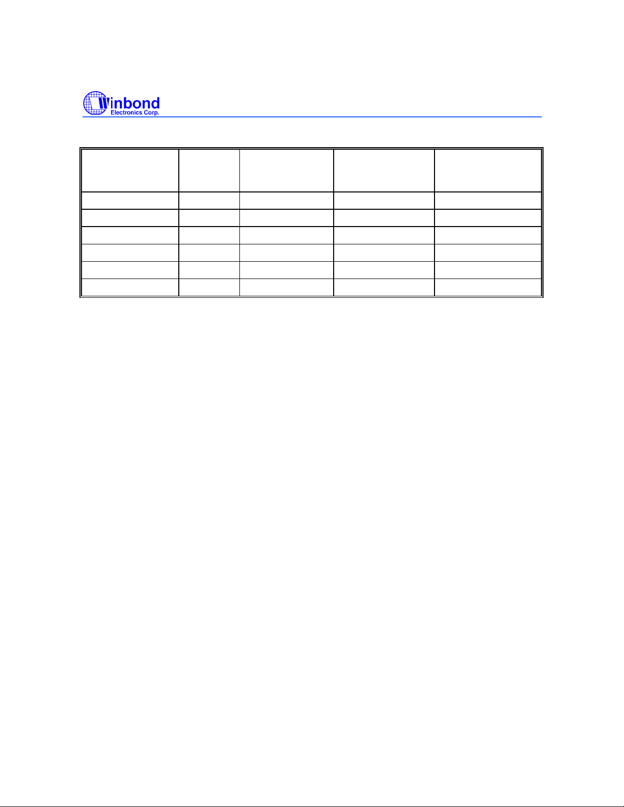
ORDERING INFORMATION
W27E257
PART NO. ACCESS
TIME (nS)
W27E257-10 100 30 100 600 mil DIP
W27E257-12 120 30 100 600 mil DIP
W27E257-15 150 30 100 600 mil DIP
W27E257P-10 100 30 100 32-pin PLCC
W27E257P-12 120 30 100 32-pin PLCC
W27E257P-15 150 30 100 32-pin PLCC
Notes:
1. Winbond reserves the right to make changes to its products without prior notice.
2. Purchasers are responsible for performing appropriate quality assurance testing on products intended for use in
applications where personal injury might occur as a consequence of product failure.
POWER SUPPLY
CURRENT MAX.
(mA)
STANDBY VCC
CURRENT MAX.
(µA)
PACKAGE
- 12 -
Page 13
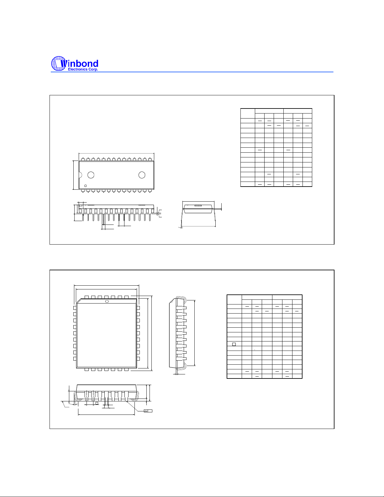
PACKAGE DIMENSIONS
28-pin P-DIP
28
E
1
1
S
2
A
A
L
D
B
e
1
B
1
W27E257
Dimension in Inches Dimension in mm
Symbol
Min. Nom. Max. Max.Nom.Min.
A
0.010
1
A
0.150
A
2
0.016
B
1
B
0.008
c
D
15
14
Base Plane
1A
E
c
Seating Plane
e
a
A
E
0.540
1
E
0.090
e
1
0.120
L
a
A
e
S
Notes:
1. Dimension D Max. & S include mold flash or
tie bar burrs.
2. Dimension E1 does not include interlead flash.
3. Dimension D & E1 include mold mismatch and
are determined at the mold parting line.
4. Dimension B1 does not include dambar
protrusion/intrusion.
5. Controlling dimension: Inches.
6. General appearance spec. should be based on
final visual inspection spec.
0.210
0.155
0.160
0.018
0.022
0.060 1.52
0.0640.058
0.010
0.014
1.460 1.470
0.610
0.6000.590
0.5500.545
0.110
0.100
0.140
0.130
0 15
0.670
0.6500.630 16.00 16.51
0.090
14.99
13.72 13.9713.84
5.33
0.25
3.81
3.94
2.29
3.05
0.46
0.25
37.08
15.24
2.54 2.79
3.30
4.06
0.56
1.631.47
0.36
37.34
15.49
3.56
17.02
2.29
150
0.41
0.20
32-pin PLCC
5
13
14 20
L
θ
Seating Plane
H
E
E
1
324
30
29
D
D
D
H
21
G
c
Symbol
A
A
A
b
b
c
D
E
e
G
G
H
H
L
y
θ
1
2
1
D
E
D
E
Dimension in Inches
Min. Nom. Max. Max.Nom.Min.
0.020
0.028
0.016
0.018
0.008
0.010
0.547
0.550
0.447
0.450
0.050
0.490
0.51
0.390
0.410
0.585
0.590
0.485
0.49
0.075
0.090
°
0
0.140
0.1150.105 0.110
0.0320.026
0.022
0.014
0.553
0.453
0.530
0.430
0.595
0.495
0.095
0.004
°
10
Dimension in mm
0.50
2.802.67 2.93
0.66 0.81
0.71
0.41
0.46
0.20
0.25
13.89
13.97
11.35
11.43
1.27
1.12 1.420.044 0.056
12.45 12.9
9.91
10.41
14.86
14.99
12.32
12.45
1.91 2.29
°
0
3.56
0.56
0.35
14.05
11.51
13.46
10.92
15.11
12.57
2.41
0.10
°
10
Notes:
2
A
A
e
b
b
1
E
G
1
A
y
1. Dimension D & E do not include interlead flash.
2. Dimension b does not include dambar protrusion/intrusion.
3. Controlling dimension: Inches.
4. General appearance spec. should be based on final
visual inspection sepc.
Publication Release Date: January 1997
- 13 - Revision A3
Page 14

W27E257
Headquarters
No. 4, Creation Rd. III,
Science-Based Industrial Park,
Hsinchu, Taiwan
TEL: 886-3-5770066
FAX: 886-3-5792647
http://www.winbond.com.tw/
Voice & Fax-on-demand: 886-2-7197006
Winbond Electronics (H.K.) Ltd.
Rm. 803, World Trade Square, Tower II,
123 Hoi Bun Rd., Kwun Tong,
Kowloon, Hong Kong
TEL: 852-27513100
FAX: 852-27552064
Taipei Office
11F, No. 115, Sec. 3, Min-Sheng East Rd.,
Taipei, Taiwan
TEL: 886-2-7190505
FAX: 886-2-7197502
Note: All data and specifications are subject to change without notice.
- 14 -
Winbond Electronics North America Corp.
Winbond Memory Lab.
Winbond Microelectronics Corp.
Winbond Systems Lab.
2730 Orchard Parkway, San Jose,
CA 95134, U.S.A.
TEL: 1-408-9436666
FAX: 1-408-9436668
 Loading...