

Page 1
W166
Spread Spectrum Frequency Timing Generator
Features
is greatly reduced. Use of this technology allows systems to
pass increasi ngly diffi cult EMI testi ng without res orting to cost-
• Maximized EMI suppression usi ng Cypress’s Spread
Spec trum te chnol ogy
• Generates a spread spectrum copy of the provided
input
• Selectable spreading characteristics
• Integrated loop filter components
• Operates with a 3.3V or 5V supply
• SSON# pin enables frequenc y spreading
• Low po w er CMOS design
• Available in 8-pin SOIC (Small Outline Integrated
Circuit)
Overview
ly shielding or redesign.
In a system, not on ly is EMI reduced i n the v ari ous cl oc k lin es,
but also in all signals which are synchronized to the clock.
Therefore, the benefits of using this technology increase with
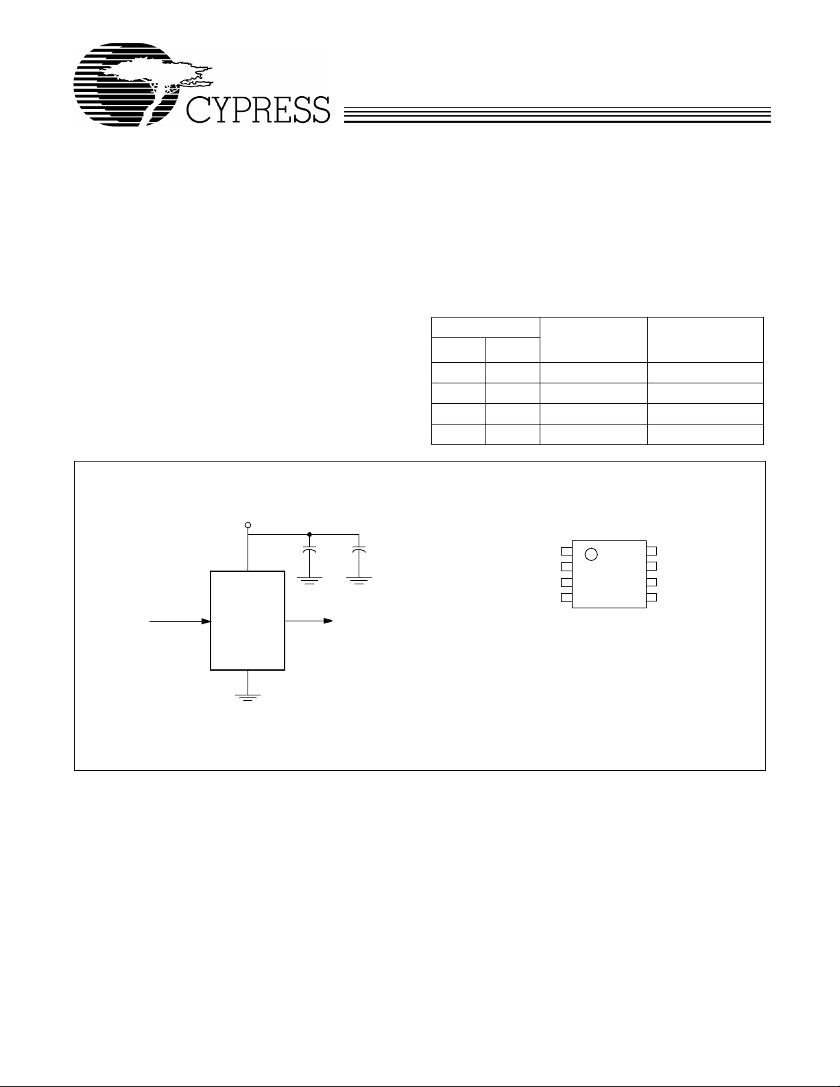
the number of address and data lines in the system. The Simplified Block Diagram shows a simple implementation.
T able 1. Frequency Spread Selection
W166 Input
Frequency
(MHz)
0 0 50 to 65 f
0 1 50 to 65 f
The W166 incorporates the latest advances in PLL spread
spectrum frequency synthesizer techniques. By frequency
modulating the output with a low-frequency carrier, peak EMI
1 0 50 to 65 f
1 1 50 to 65 f
Simplified Block Diagram Pin Configuration
3.3V or 5V
Oscillator or Reference
Input
W166
Spread Spectrum
(EMI suppressed)
Output
CLKIN
GND
NC
FS1
1
2
3
4
Output
Frequency (MHz)FS1 FS0
±0.625%
IN
±1.25%
IN
±2.5%
IN
–3.75%
IN
SSON#
8
W166
7
6
5
CLKOUT
FS0
VDD
Cypress Semiconductor Corporation
• 3901 North First Street • San Jose • CA 95134 • 408-943-2600
December 20, 1999, rev. **
Page 2
Pin Definitions
Pin Name Pin No.
CLKOUT 7 O
CLKIN 1 I
NC 2 NC
SSON# 8 I
FS0:1 6, 4 I
VDD 5 P
GND 3 G
Pin
T ype Pin Description
Output Modulated Freque ncy
: Frequency modulated copy of the reference input
(SSON# asserted).
External Reference Frequency Input:
No Connect:
This pin must be left unconnected.
Spread Spectrum Control (Active LOW):
Clock input.
Asserting this signal (a cti ve LOW) turns the
internal modulation waveform on. This pin has an internal pull-down resistor.
Frequency Selecti on Bit s 0,1:
These pins select the frequency spreading characteris-
tics. Refer to Table 1 . These pins have internal pull-up resistors.
Power Connection:
Ground Connection:
Connected to 3.3V or 5V power supply.
This should be connected to t he common ground pl ane.
W166
Functional Description
The W166 uses a Phase-Locked Loop (PLL) to frequency
modulate an input clock. The result is an output clock whose
frequency is slowly swept over a narrow band near the input
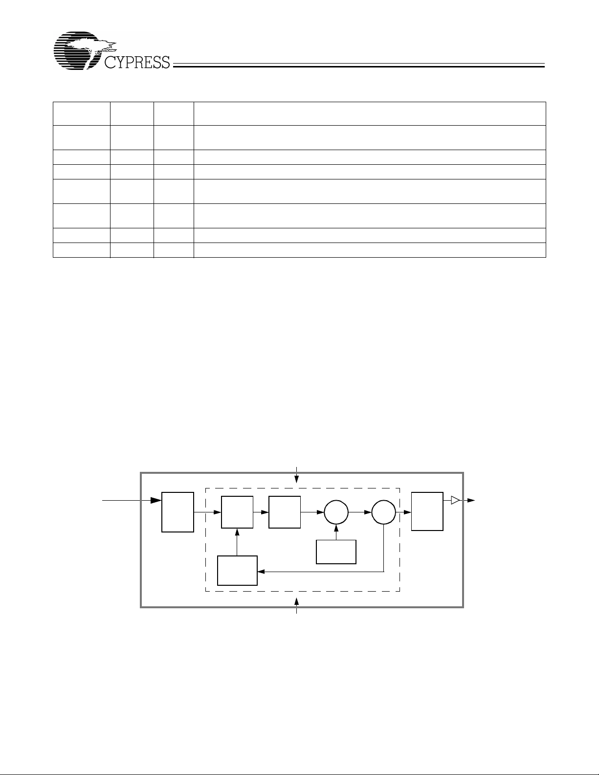
signal. The basic circuit topology is shown in Figure 1. The
input reference signal is divided by Q and fed to the phase
detector. A signal from the VCO is divided by P and fed back
to the phase detec tor al so . The PLL will f or ce the fr equency of
the VCO output sign al to change until the divid ed output signal
and the divided reference signal match at the phase detector
input. The output frequency is then equal to the ratio of P/Q
times the r efe renc e freq uency. (Note: F o r the W166 the output
frequency i s equal to the input frequenc y.) The uni que feature
of the Spread Spec trum F re quency Ti ming Generat or is t hat a
modulating w av eform i s superimposed at the i nput to t he VCO .
This causes the VCO output to be slowly swept across a predetermined frequen cy band.
Clock Input
Reference Input (EMI suppressed)
Freq. Phase
Q
Detector
Feedback
Divider
P
Charge
Pump
Because the modulating frequency is typically 1000 times
slower than the fundamental clock, the spread spectrum process has little impact on system performance.
Frequency Selection With SSFTG
In Spread Spectrum Frequency Timing Generati on, EMI reduction depends on the shape, modulation percentage, and
frequency of the modulating waveform. While the shape and
frequency of the modulating waveform are fixed, the modulation percentage may be varied.
A larger spreading per centage improves EMI reduction . However, large spread percentages may either exceed system
maximum frequ ency ra tings or lo wer the a v erag e fr equency t o
a point where perf ormance is af fect ed. For these reasons , narrow and wide modulation selections are provided.
VDD
CLKOUT
Σ
Modulating
Waveform
VCO
Post
DividersDivider
PLL
GND
Figure 1. System Block Diagram
2
Page 3
W166
Spread Spectrum Frequency Tim ing G enera to r
The device generates a clock that is frequency modulated in
order to increase the bandwidth that it occu pies. By increas ing
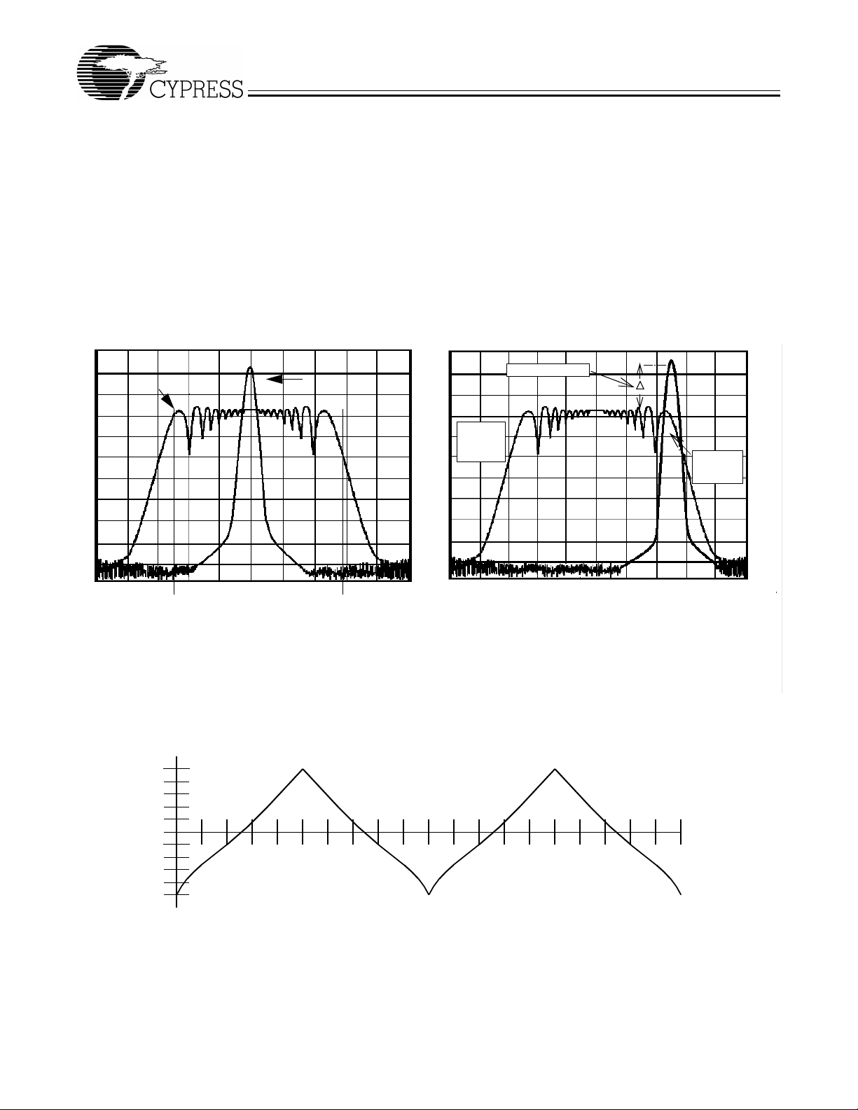
the bandwidth of the fundamental and i ts harmonics, the amplitudes of the radiated electromagnetic emissions are reduced. This effect is depicted in Figure 2.
As shown in Figure 2, a harmonic of a modulated clock has a
much low er amplitu de than that of an un modulated si gnal. The
reduction in amplitude is dependent on the harmonic number
and the frequency deviation or spr ead. The equation for the
reduction is
dB = 6.5 + 9*log
SSFTG Typical Clock
Amp litu d e (d B )
(P) + 9*log10(F)
10
Where P is the percenta ge of de vi ation and F is the frequen cy
in MHz where the reduction is measured.
The output clock is modulated with a waveform depicted in
Figure 3. This waveform , as discussed in “Spread Spectrum
Clock Generation f or the Reducti on of Radiated Emissio ns” by
Bush, Fessler, and Hardin produces the maximum reduction
in the amplitude of radiated electromagnetic emissions. The
deviati on selected for t his chip is ±0. 45% or 0. 6% of the sel ected frequency. Figure 3 details the Cypress spreading pattern.
Cypress does off er optio ns with more spr ead and great er EMI
reduction. Contact your local Sales representative for details
on these devices.
EM I Reduction
Spread
Spectrum
Enabled
Amplitude (dB)
Non-
Spread
Spectrum
Frequency Span (MH z)
Center Sp read
Frequency Span (MHz)
Down Spread
Figure 2. Clock Harmonic wi th and without SSCG Modul ation Freq uency Domain Repre sentation
MAX.
10%
20%
30%
40%
50%
60%
70%
80%
FREQUENCY
MIN.
90%
100%
10%
20%
30%
40%
50%
60%
70%
80%
Figure 3. Typica l Modulation Profile
90%
100%
3
Page 4
Absolute Maximum Ratings
W166
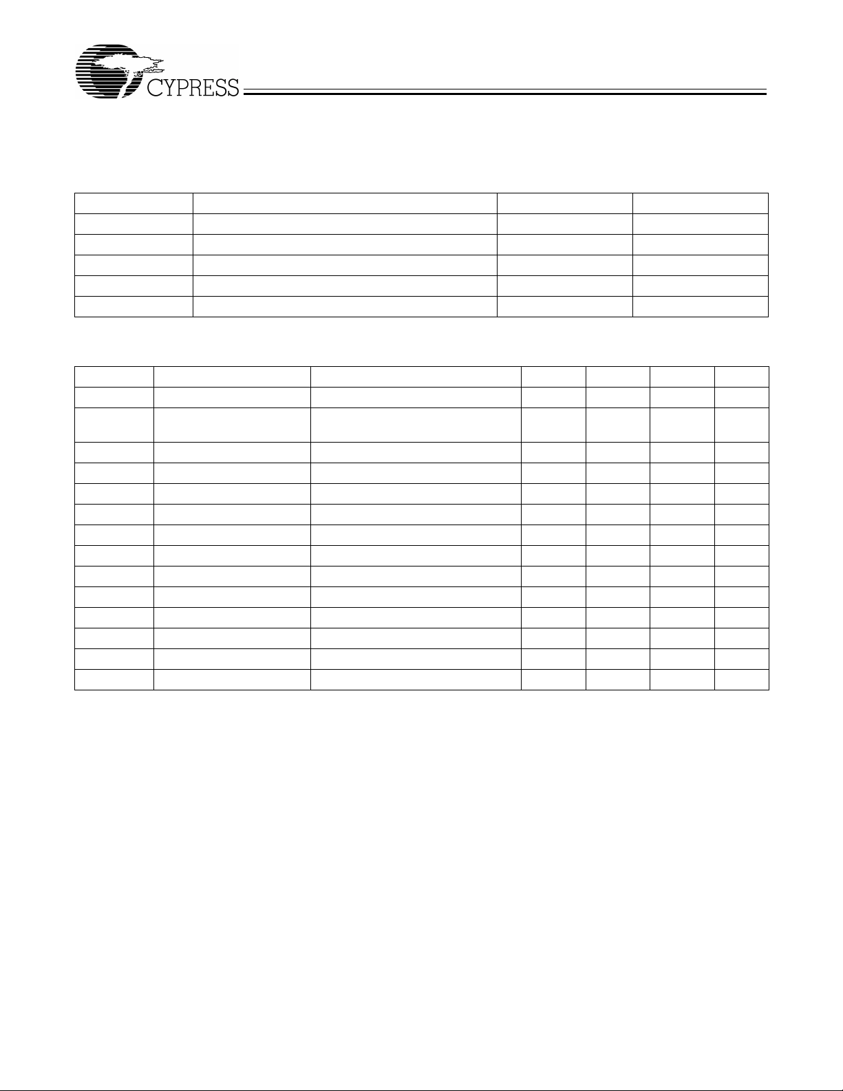
Stresses gre ater th an those li sted i n this tab le may cause permanent damage to the de vice. These represent a stress ratin g
only. Operation of the device at these or any other conditions
.
above those specified in the operating secti ons of this specification is not implied. Maximum conditions for extended per iods may affect reliability
Parameter Description Rating Unit
V
, V
DD
IN
T
STG
T
A
T
B
P
D
DC Electr i cal C h ar acteristics
Voltage on any Pin with Respect to GND –0.5 to +7 .0 V
Storage Temperature –65 to +150 °C
Operating Temperature 0 to +70 °C
Ambient Temperature under Bias –55 to +125 °C
Power Dissipation 0.5 W
:
0°C < T
< 70°C, VDD = 3.3V ±5%
A
Parameter Description Test Condition Min Typ Max Unit
I
DD
t
ON
V
IL
V
IH
V
OL
V
OH
I
IL
I
IH
I
OL
I
OH
C
I
C
I
R
P
Z
OUT
Note:
1. Inputs FS1:0 have a pull-up resistor, Input SSON# has a pull-down resistor.
Supply Current 18 32 mA
Power Up Time First locked clock cycle after Power
5ms
Good
Input Low Voltage 0.8 V
Input High Voltage 2.4 V
Output Low Voltage 0.4 V
Output High Voltage 2.4 V
Input Low Current Note 1 –20 µA
Input High Current Note 1 20 µA
Output Low Current @ 0.4V, VDD = 3.3V 15 mA
Output High Current @ 2.4V, VDD = 3.3V 15 mA
Input Capacitance All pins except CLKIN 7 pF
Input Capacit ance CLKIN pin only 6 5 pF
Input Pull-Up Resistor 500 kΩ
Clock Output I mp edance 25 Ω
4
Page 5
W166
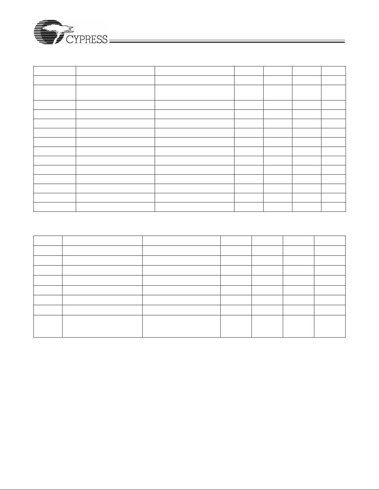
DC Electr i cal C h ar acteristics:
0°C < T
< 70°C, VDD = 5V ±10%
A
Parameter Description Test Condition Min Typ Max Unit
I
DD
t
ON
V
IL
V
IH
V
OL
V
OH
I
IL
I
IH
I
OL
I
OH
C
I
C
I
R
P
Z
OUT
AC Electrical Characteristics:
Supply Current 21 40 mA
Power Up Time Firs t locked clo ck c yc l e after
5ms
Powe r Good
Input Low Voltage 0.8 V
Input High Voltage 3.5 V
Output Low Voltage 0.4 V
Output High Voltage 2.4 V
Input Low Current Note 1 –20 µA
Input High Current Note 1 20 µA
Output Low Current @ 0.4V, VDD = 5V 24 mA
Output High Current @ 2.4V, VDD = 5V 24 mA
Input Capacit ance All pins except CLKIN 7 pF
Input Capacit ance CLKIN pin only 5 pF
Input Pull-Up Resistor 500 kΩ
Clock Output Impedance 25 Ω
TA = 0°C to +70°C, VDD = 3.3V ±5% or 5V±10%
Symbol Parameter Test Condition Min Typ Max Unit
f
IN
f
OUT
t
R
t
F
t
OD
t
ID
t
JCYC
Input Frequency Input Clock 50 65 MHz
Output Frequency Spread Off 50 65 MHz
Output Rise Time 15-pF load, 0.8V–2.4V 2 5 ns
Output Fall Time 15-pF load, 2.4V–0.8V 2 5 ns
Output Duty Cycle 15-pF load, test at VDD/2 40 60 %
Input Duty Cycle 40 60 %
Jitter, Cycle- to - C yc le 250 300 ps
Harmonic Reduction f
= 50 MHz, thir d harmonic
out
measured, reference board,
8dB
15-pF load
5
Page 6
W166
Application Information
Recommended Circuit Configurati on
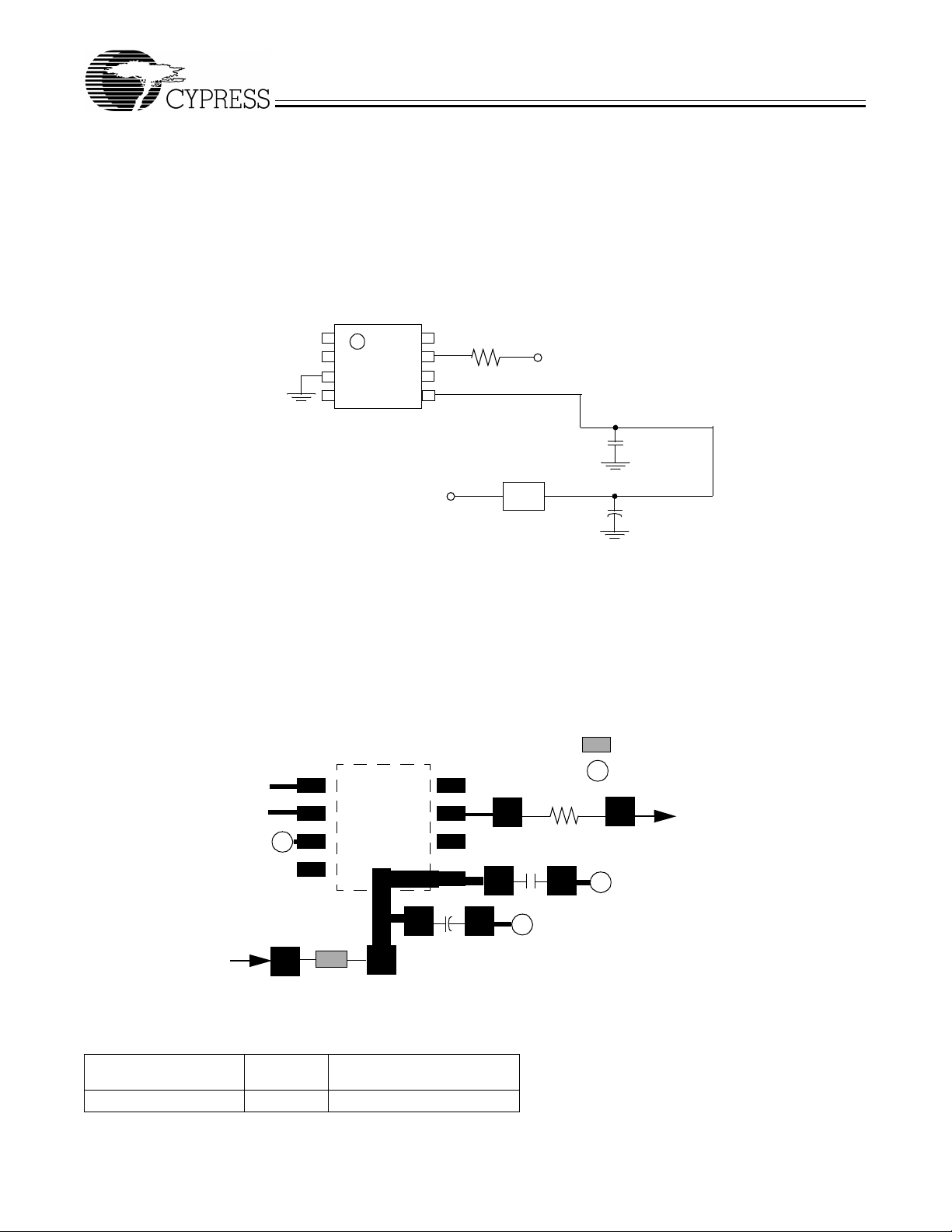
For optimum performance in system applications the power
supply decoupli ng scheme sho wn in Figure 4 should be used.
VDD decoupling i s important to both reduce phase jitter and
EMI radiation. The 0.1-µF decoupling capacitor should be
placed as close to the V
pin as possible, otherwise the in-
DD
Reference Input
NC
GND
1
2
3
4
3.3 or 5V System Supply
8
W166
7
6
5
Figure 4. Recommended Circuit Configuration
creased trace indu ctance will negate its decou pling capabili ty.
The 10-µF decoupling capacitor shown should be a tantalum
type. For further EMI protection, the V
made via a ferrite bead, as shown.
connection can be
DD
Recommended Board Layout
Figure 5 shows a recommended a 2-la yer board layout.
R1
Clock Output
VDD
C1
µF
0.1
FB
C2
µF Tantalum
10
Refer ence Input
NC
G
C2
Power Supply Input
(3.3V or 5V)
FB
Figure 5. Recommended Board Layout (2-Layer Board)
Ordering Information
Ordering Code
W166 G 8-pin Plastic SOIC (150-mil)
Package
Name Package Type
C1
G
R1
C1 =
C2 =
R1 =
FB
G
G
High frequency supply decoupling
capacitor (0.1
Common supply low frequency
decoupling capacitor (10recommended).
Match valu e to li ne imp e d an ce
Ferrite Bead
=
=
Via To GND Plane
µF recommended).
Clock Output
µF tantalum
Document: #38-00878
6
Page 7
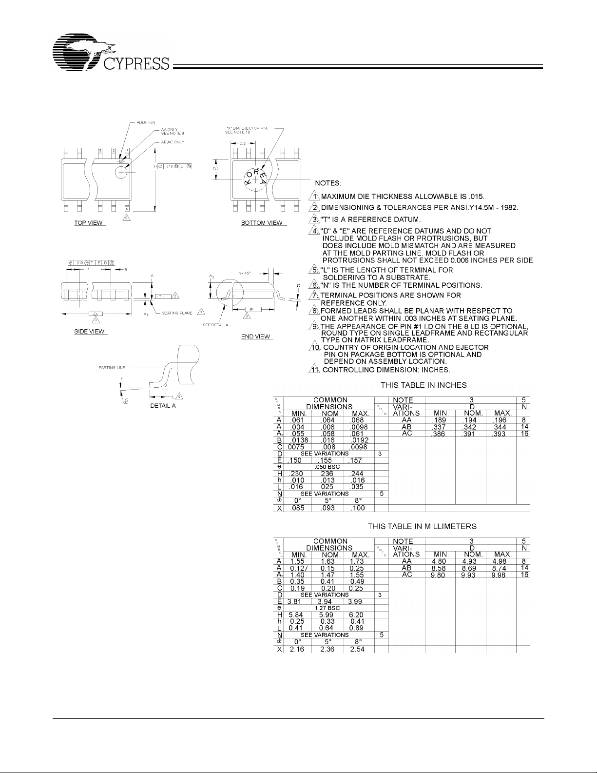
Package Diagram
W166
8-Pin Small Outlined Integrat ed Circuit (SOIC, 150-mil)
© Cypress Semiconductor Corporation, 1999. The information contained herein is subject to change without notice. Cypress Semiconductor Corporation assumes no respons ibility for the use
of any circuitry other than circuitry embodied in a Cypress Semiconductor product. Nor does it con vey or imply any lice nse under patent or other rights. Cypress Semicondu ctor does not authorize
its products for use as critical components in life-support systems where a malfunction or failure may reasonably be expected to result in significant injury to the user. The inclusion of Cypress
Semiconductor products in l ife-support systems application implies that the manufacturer assumes all risk of such use and in doing so indemnifies Cypress Semiconductor against all charges.
 Loading...