

Page 1
Rectifier Diode
Types W0507YH360 to W0507YH450
The data sheet on the subsequent pages of this document is a scanned copy of existing
data for this product.
(Rating Report 96D04 Issue 2)
This data reflects the old part number for this product which is: SW36-45HXC270. This part
number must NOT be used for ordering purposes – please use the ordering particulars
detailed below.
The limitations of this data are as follows:
No reverse recovery information available
Please use the following link to view an up to date outline drawing for this device
Outline W3
Where any information on the product matrix page differs from that in the following data,
the product matrix must be consider ed cor r ect
An electronic data sheet for this product is presently in preparation.
For further information on this product, please contact your local ASM or distributor.
Alternatively, please contact Westcode as detailed below.
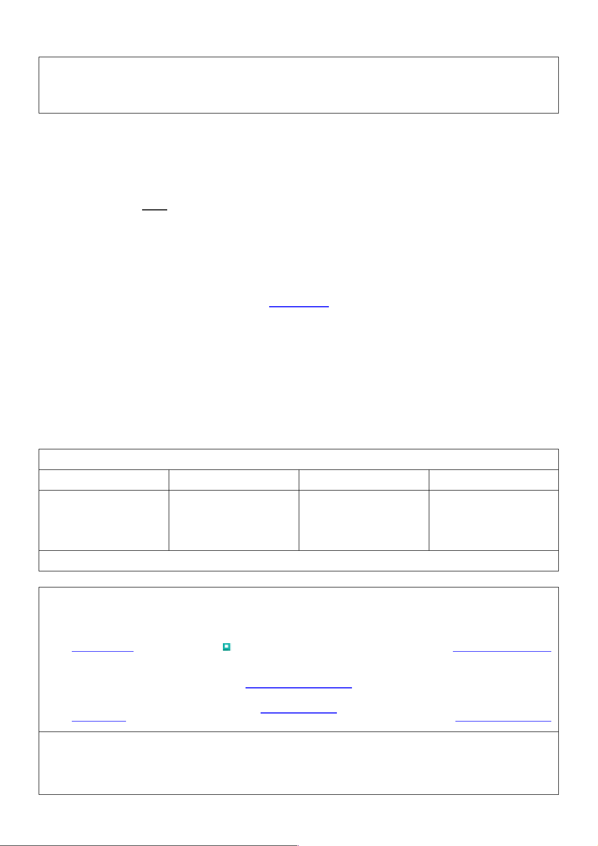
Ordering Particulars
W0507 YH
Fixed Type Code Fixed Outline Code
Typical Order Code: W0507YH380, 26.6mm clamp height, 3800V V
IXYS Semiconductor GmbH
Edisonstraße 15
D-68623 Lampertheim
Tel: +49 6206 503-0
Fax: +49 6206 503-627
E-mail: [email protected]
WESTCODE
An IXYS Company
Voltage code
V
/100
RRM
36-45
0
Fixed Code
RRM
Westcode Semiconductors Ltd
Langley Park Way, Langley Park,
Chippenham, Wiltshire, SN15 1GE.
Tel: +44 (0)1249 444524
Fax: +44 (0)1249 659448
E-mail: [email protected]
IXYS Corporation
3540 Bassett Street
Santa Clara CA 95054 USA
Tel: +1 (408) 982 0700
Fax: +1 (408) 496 0670
E-mail: [email protected]
The information contained herein is confidential and is protected by Copyright. The information may not be used or disclosed except with the written
permission of and in the manner permitted by the proprietors Westcode Semiconductors Ltd.
In the interest of product improvement, Westcode reserves the right to change specifications at any time without prior notice.
Devices with a suffix code (2-letter, 3-letter or letter/digit/letter combination) added to their generic code are not necessarily subject to the conditions
and limits contained in this report.
www.westcode.com
www.ixys.com
E-mail: [email protected]
Westcode Semiconductors Inc
3270 Cherry Avenue
Long Beach CA 90807 USA
Tel: +1 (562) 595 6971
Fax: +1 (562) 595 8182
© Westcode Semiconductors Ltd.
Page 2
QUALITY AND EVALUATION LABORATORY
Rating Report No: 96D04 Issue 2 Date: 17th March, 1999
Origin: PAR99009 Pages: 11
Capsule Diode Type SW36-45HXC270
Author: W. Findlay Checked: Approved:
1. Abstract
The HXC270 rectifier diode features a 30mm diameter silicon slice (manufacturing reference DANXH)
mounted in a cold weld capsule.
Summary of changes to previous issue.
Issue 1 Advance Data
Issue 2 Full Rating
The information contained herein is confidential and is protected by Copyright. The information may not be
used or disclosed except with the written permission of and in the manner permitted by the proprietors
Westcode Semiconductors Ltd.
In the interest of product improvement, Westcode reserves the right to change specifications at any time
without prior notice.
SW36-45HXC270 Rating Report 96D04 Issue 2, March 99 page 1 of 11
Page 3

2. Contents
1.0 Abstract 1
2.0 Contents 2
3.0 Introduction 2
4.0 Maximum Ratings 3
5.0 Characteristics 4
6.0 Notes on Ratings and Characteristics
6.1 Voltage Grade Table 5
6.2 Extension of Voltage Grades 5
6.3 De-Rating Factor 5
6.4 Computer Modelling Parameters
6.4.1 Device Dissipation Calculations 5
6.4.2 ABCD Coefficients 6
6.4.3 Thermal Impedance Calculations 6
7.0 Curves
Figure 1 – Mean Forward Current vs. Maximum Power Dissipation, Double Side Cooled 7
Figure 2 – Mean Forward Current vs. Maximum Heatsink Temp, Double Side Cooled 7
Figure 3 – Mean Forward Current vs. Maximum Power Dissipation, Single Side Cooled 8
Figure 4 - Mean Forward Current vs. Maximum Heatsink Temp, Single Side Cooled 8
Figure 5 – Limit Forward Voltage Characteristics 9
Figure 6 – Transient Thermal Impedance 9
2
Figure 7 – Surge Current and I
t vs. Duration of Surge 10
8.0 Layout Drawing and Ordering Information 11
3. Introduction
The HXC270 rectifier diode features a 30mm diameter silicon slice mounted in a cold weld capsule.
SW36-45HXC270 Rating Report 96D04 Issue 2, March 99 page 2 of 11
Page 4
4.0 Maximum Ratings
VOLTAGE RATINGS
V
RRM
V
RSM
Repetitive peak reverse voltage, (note 1). 3600-4500 V
Non-repetitive peak reverse voltage, (note 1). 3700-4600 V
RATINGS
I
F(AV)
I
F(AV)
I
F(AV)
I
F(RMS)
I
F(d.c.)
I
FSM
I
FSM2
I2tI
I2t
T
HS
T
stg
Mean on-state current, Tsink=55°C, (note 2). 505 A
Mean on-state current. Tsink=100°C, (note 2). 345 A
Mean on-state current. Tsink=100°C, (note 3). 210 A
Nominal RMS on-state current, 25°C, (note 2). 935 A
D.C. on-state current, 25°C, (note 5). 805 A
Peak non-repetitive surge tP=10ms, VRM=0.6V
Peak non-repetitive surge tP=10ms, VRM≤10V, (note 4).
2
t capacity for fusing tP=10ms, VRM=0.6V
I2t capacity for fusing tP=10ms, VRM≤10V, (note 4).
Operating temperature range. -40 to +160 °C
Storage temperature range. -55 to +160 °C
Capsule Diode
Types SW36-45HXC270
MAXIMUM
MAXIMUM
, (note 4). 7600 A
RRM
, (note 4). 289 × 10
RRM
Date :- March 99
Rat. Rep:- 96D04
Issue:- 2
LIMITS
LIMITS
8200 A
3
336 × 10
3
UNITS
UNITS
A2s
A2s
Notes:
1) De-rating factor of 0.13% per °C is applicable for T
2) Double side cooled, single phase; 50Hz, 180° half-sine wave.
3) Single side cooled, single phase; 50Hz, 180° half-sine wave.
4) Half-sinewave, 160°C T
initial.
j
below 25°C.
j
5) Double Side Cooled.
SW36-45HXC270 Rating Report 96D04 Issue 2, March 99 page 3 of 11
Page 5
5.0 Characteristics
CHARACTERISTICS MIN TYP MAX TEST CONDITIONS
=635A.
V
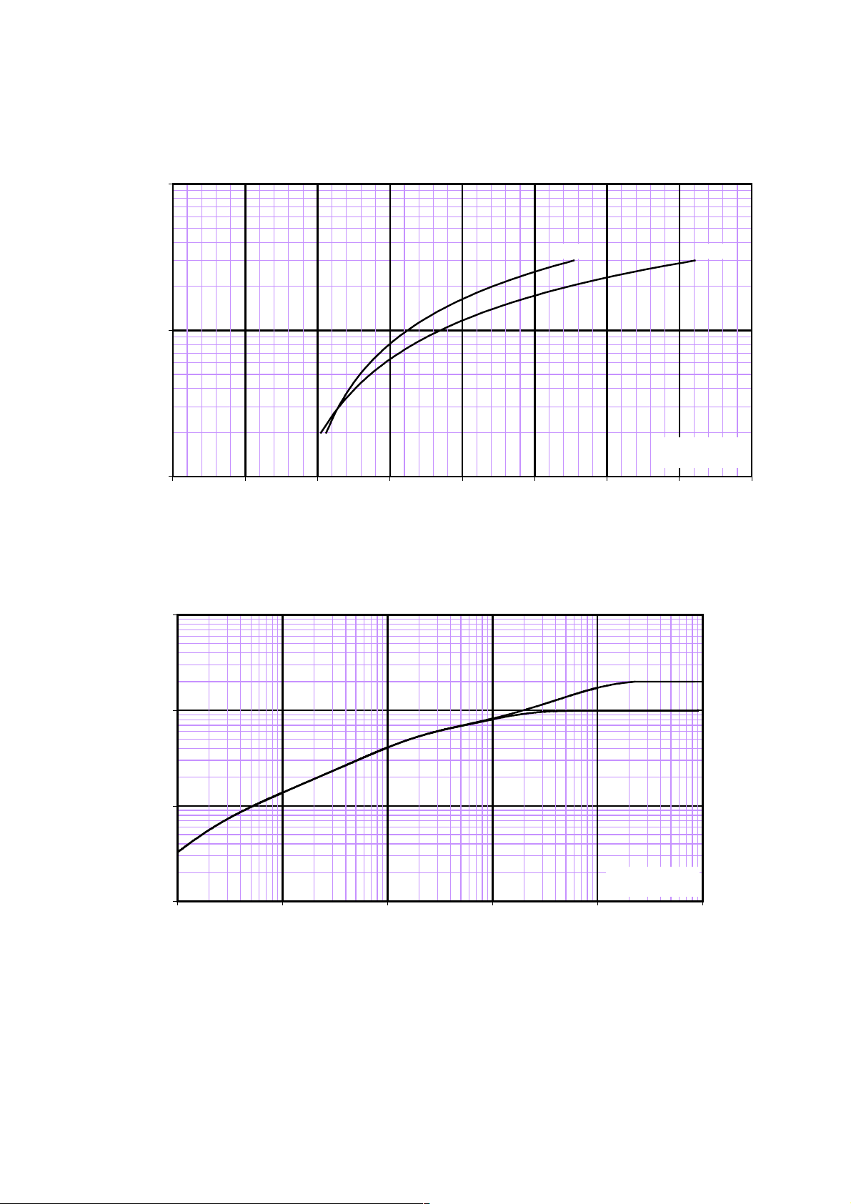
Maximum peak forward voltage. - - 1.50
FM
V
Threshold voltage. - - 0.97 V
0
r
Slope resistance. - - 0.88
S
I
Peak reverse current. - - 30
RRM
Thermal resistance junction to
R
θ
sink.
- - 0.1 Double side cooled. °C/W
- - 0.2 Single side cooled. °C/W
I
F
Rated V
RRM
UNITS
V
mΩ
mA
F Mounting force. 3.3 - 5.5 kN
WtWeight. - 140 - g
Notes:-
1) Unl ess otherwise indicated T
=160°C.
j
SW36-45HXC270 Rating Report 96D04 Issue 2, March 99 page 4 of 11
Page 6
6.0 Notes on ratings and characteristics
f
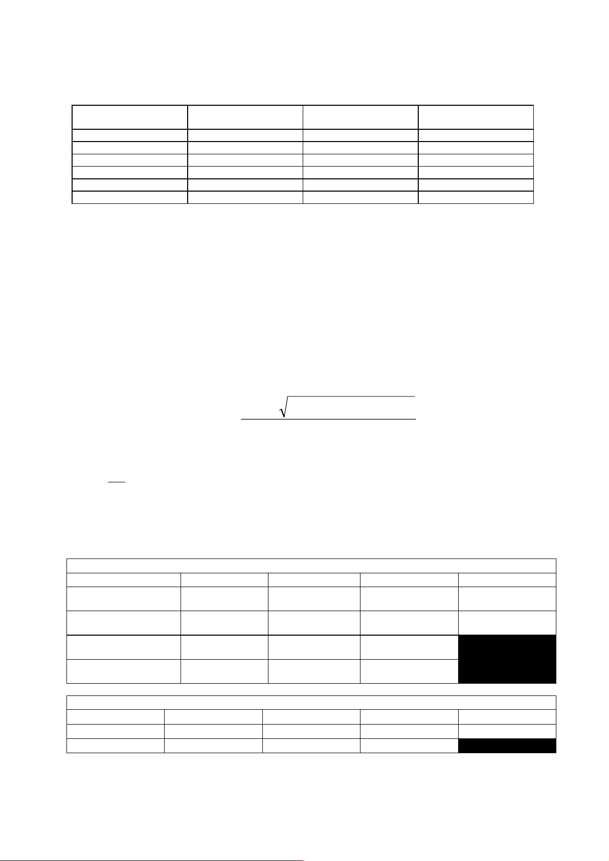
6.1 Voltage grade table
Voltage Grade 'H' V
36 3600 3700 1900
38 3800 3900 1950
40 4000 4100 2000
42 4200 4300 2040
44 4400 4500 2080
45 4500 4600 2100
6.2 Extension of voltage grades
This report is applicable to other and higher voltage grades when supply has been agreed by
Sales/Production.
6.3 De-rating factor
A blocking voltage de-rating factor of 0.13% per deg Celsius is applicable to this device for Tj
25°C.
6.4 Computer modelling parameters
6.4.1 Device dissipation calculations
I
Where Vo= 0.97 V, rs=0.88 mΩ
AV
RRM
V
2
++−
=
V
RSM
V
2
2
rff
**2
s
WrffVV
***4
AVsoo
V
R
D.C.
below
T
W
R
Square wave Double
Side Cooled
Square wave Single
Side Cooled
Sine wave Double
Side Cooled
Sine wave Single Side
Cooled
Conduction Angle
Square wave 2.45 1.73 1.41 1
Sine wave 2.78 1.88 1.57
∆
=
AV
R
th
= Supplementary thermal impedance, see table below.
th
f
= Form factor, see table below.
Conduction Angle 6 phase (60°) 3 phase (120°) Half wave (180°) d.c.
∆Tt t
=−
jMax HS
Supplementary Thermal Impedance
0.130 0.117 0.110 0.1
0.230 0.217 0.210 0.2
0.117 0.108 0.103
0.217 0.208 0.203
o
60
Form Factors
120
o
180
o
d.c.
SW36-45HXC270 Rating Report 96D04 Issue 2, March 99 page 5 of 11
Page 7
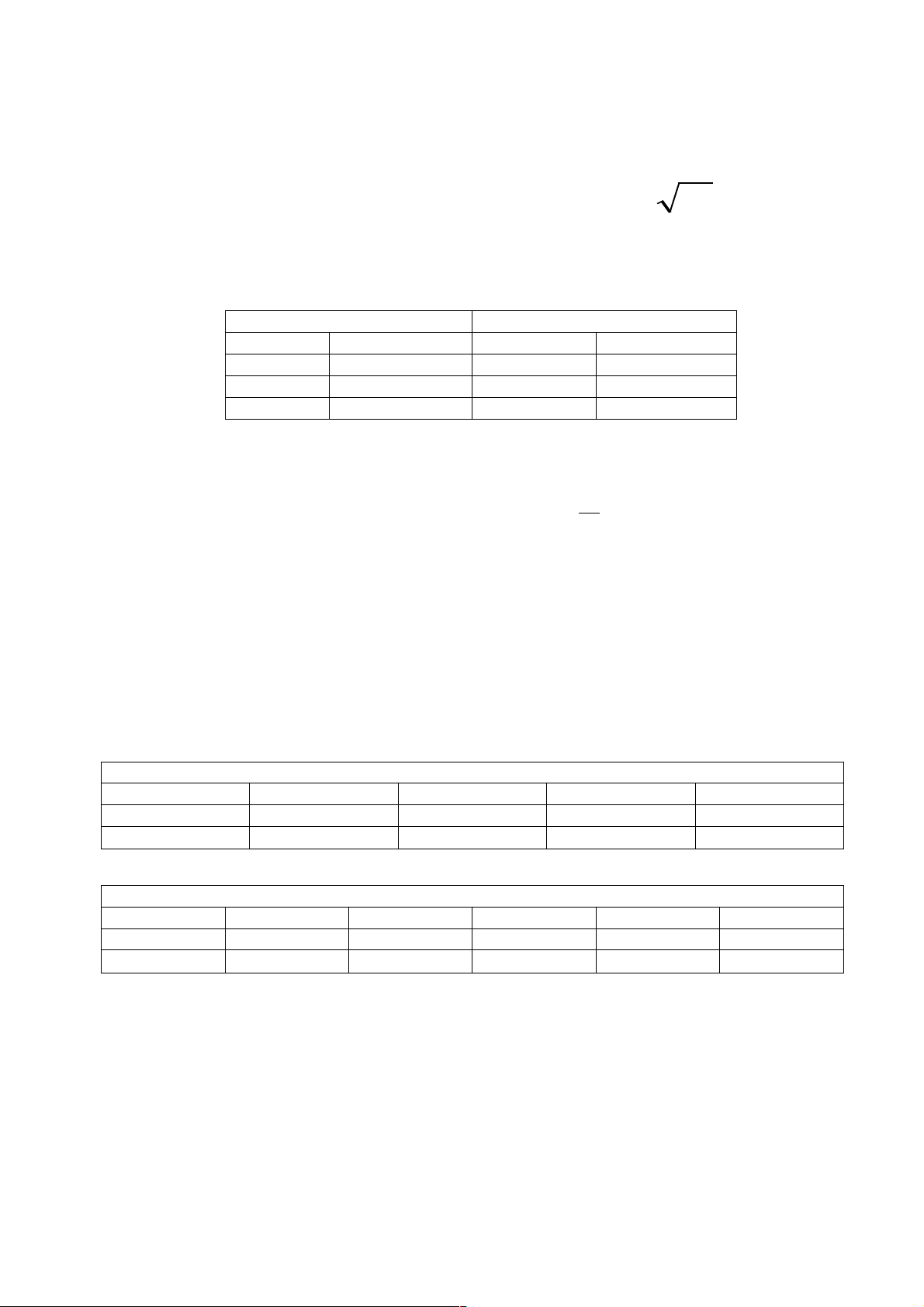
6.4.2 ABCD Coefficients
The on-state characteristic I
used for rating purposes and (ii) a set of constants A, B, C, D, forming the coefficients of the
representative equation for V
The constants, derived by curve fitting software, are given in this report for both hot and cold
characteristics where possible. The resulting values for V
limited current range which is generally that over which the curve is plotted.
6.4.3 Thermal impedance calculations
vs. VF is represented in two ways; (i) the well established Vo and rs tangent
F
in terms of IF given as:
F
FFFF ID.)C.(I)(IB.AV +++= ln
agree with the true device characteristic over a
F
160°C Coefficients 25°C Coefficients
A 0.2587428 A 0.6783057
B 0.1185595 B 0.03467407
C 8.401342 × 10
D -2.233814 × 10
∑
-4
-3
=
np
pt
1
=
p
C 4.695493 × 10
D 7.388426 × 10
t
−
τ
1
err
−=
p
-4
-3
Where p = 1 to n, n is the number of terms in the series.
t = Duration of heating pulse in seconds.
= Thermal resistance at time t.
r
t
r
= Amplitude of pth term.
p
τ
= Time Constant of pth term.
p
D.C. Double Sided Cooled
Term1234
r
p
τ
p
Term 1 2 3 4 5
r
p
τ
p
0.04766233 0.03243763 9.409791 × 10
1.066889 0.1235431 0.03840402 3.538193 × 10
D.C. Single Side Cooled
0.1366152 0.0151329 0.0383066 8.577754 × 10
6.983036 0.8476553 0.1217136 0.0159452 2.446305 × 10
-3
-3
9.611571 × 10
6.230917 × 10
-3
-3
-3
-3
SW36-45HXC270 Rating Report 96D04 Issue 2, March 99 page 6 of 11
Page 8
7.0 Curves
k
1600
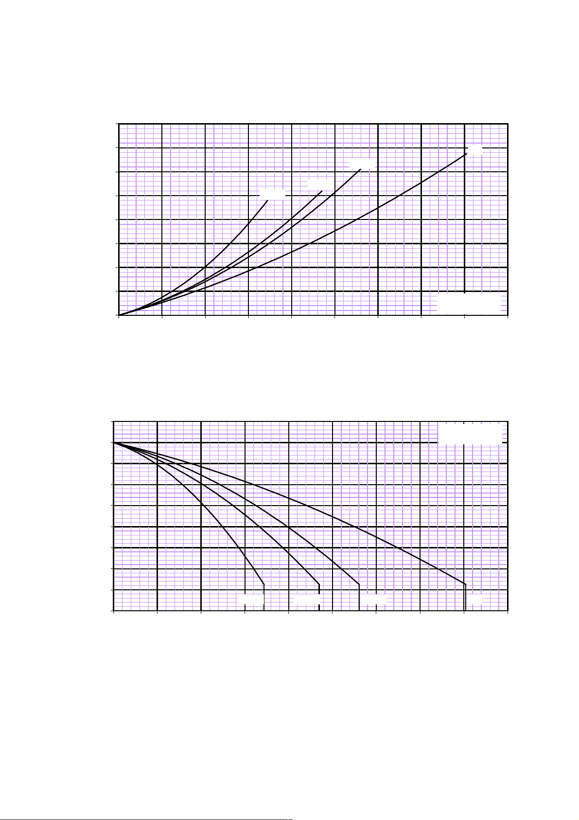
Figure 1 - Mean forward current vs. Power dissipation - Double side cooled
Maximum Forward Dissipation (W)
180
160
1400
1200
½ wave
3 phase
1000
6 phase
800
600
400
200
0
SW36-45HXC270
96D04 Issue 2
0 100 200 300 400 500 600 700 800 900
Mean Forward Current (A) (Whole cycle averaged)
Figure 2 - Maximum permissable heatsink temperature vs. forw ard
current - Double side cooled
SW36-45HXC270
96D04 Issue 2
d.c.
140
120
100
80
temperature (°C)
60
40
Maximum permissable heatsin
20
6 phase 3 phase ½ wave d.c.
0
0 100 200 300 400 500 600 700 800 900
Mean Forward Current (A) (Whole cycle averaged)
SW36-45HXC270 Rating Report 96D04 Issue 2, March 99 page 7 of 11
Page 9
800
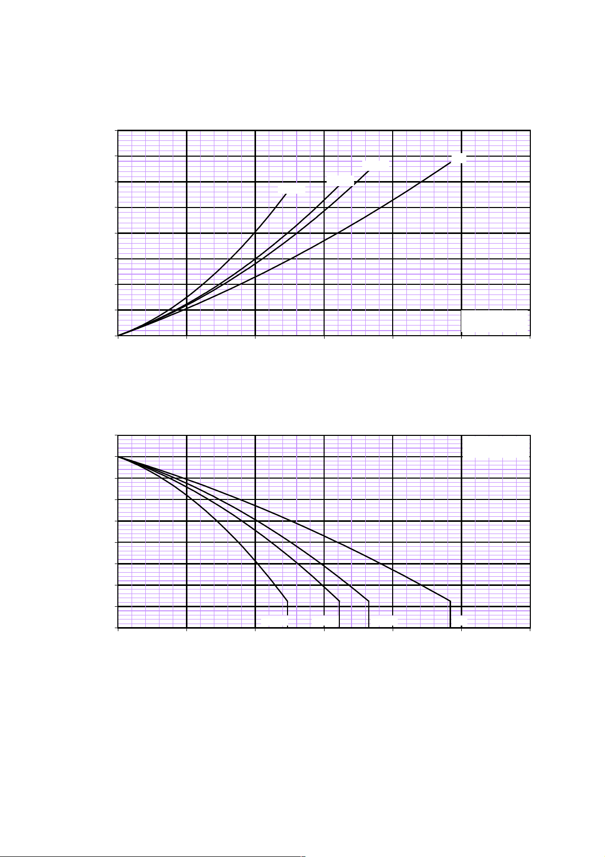
Figure 3 - Mean forward current vs. Power dissipation - Single side cooled
700
600
6 phase
½ wave
3 phase
d.c.
500
400
300
200
Maximum Forward Dissipation (W)
100
SW36-45HXC270
96D04 Issue 2
0
0 100 200 300 400 500 600
Mean Forward Current (A) (Whole cycle averaged)
Figure 4 - Maximum permissable heatsink temperature vs. forw ard
current - Single side cooled
180
160
SW36-45HXC270
96D04 Issue 2
140
120
100
80
60
40
Maximum Forward Dissipation (W)
20
6 phase 3 phase ½ wave d.c.
0
0 100 200 300 400 500 600
Mean Forward Current (A) (Whole cycle averaged)
SW36-45HXC270 Rating Report 96D04 Issue 2, March 99 page 8 of 11
Page 10
10000
)
1000
Instantaneous forward current (A
Figure 5 - Forward characteristics of limit device
160°C25°C
SW36-45HXC270
96D04 Issue 2
100
00.511.522.533.54
Maximum instantaneous forward voltage (V)
Figure 6 - Transient thermal impedance
1
0.1
0.01
Thermal impedance (°C/W)
SW36-45HXC270
96D04 Issue 2
0.001
0.001 0.01 0.1 1 10 100
Time (seconds)
SSC: 0.2°C/W
DSC: 0.1°C/W
SW36-45HXC270 Rating Report 96D04 Issue 2, March 99 page 9 of 11
Page 11
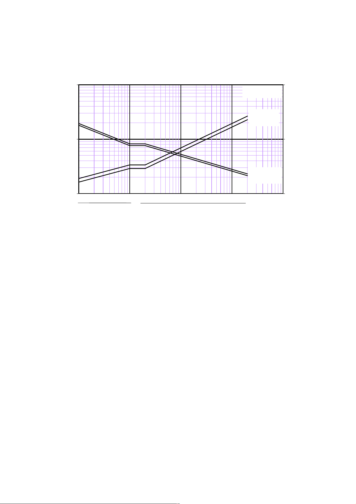
Figure 7 - Maximum non-repetitive surge current at initial junction
)
temperature 160°C
100000
10000
Total peak half sine surge current (A
1000
13510
Duration of surge (ms)
1505 10 100
Duration of surge (cycles at 50Hz )
SW36-45HXC270
96D04 Issue 2
I2t: V
=10V
RRM
2
I
t: 60%V
RRM
I
: V
RRM
: 60%V
=10V
RRM
I
FSM
FSM
1.0E+07
1.0E+06
1.0E+05
2
2
s)
t (A
Maximum I
SW36-45HXC270 Rating Report 96D04 Issue 2, March 99 page 10 of 11
Page 12
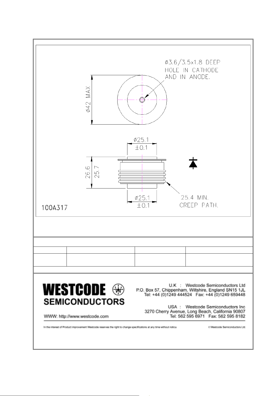
8.0 Layout Drawing and Ordering Information
ORDERING INFORMATION (Please quote 11 digit code as below)
SW
Fixed
Type Code
Typical order code : SW45HXC270 – 4.5kV V
♦♦♦♦ ♦♦♦♦
Voltage Code Fixed
HXC 270
Outline Code
Rectifier Diode, 26.6mm Clamp height capsule.
RRM
Fixed
Type Code
SW36-45HXC270 Rating Report 96D04 Issue 2, March 99 page 11 of 11
Page 13
QEL REPORTS DISTRIBUTION
Rating Report No.: 96D04 Issue 2 Date: 17th March, 1999
Author: W. Findlay Authorised by ........................
Capsule Diode
Type SW36-45HXC270
Copies Abstracts Date Dispatched
P. Leach - 1
R.A. Jones - 1
F.J. Wakeman 1 A.M. Hyde 1 E.A. Wilkins 1 A. Fowler - 1
P. Scarff 1 W.S.I. 1 -
 Loading...