

Page 1
cd34021-a.fm 15/01/98 1
VV6300 Sensor
Integrated CMOS Colour Image Sensor with
on-chip ADC.
Key Features
GENERAL DESCRIPTION
VV6300 is a highly- integra ted CMOS im age sensi ng
device. In addition to a 160 x 120 pixel image sensor
array, the device includes on-chip circuitry to drive
and sense the array.
The output stage of the sensor contains a successive
approximation circuit which performs analogue-todigital conversion of the photodiode array to produce
8-bit or 4-bit pixel data.
The primary image size is 160 x 120 but border pixels/lines can be enabled to give an effective image
size of 164 x 124.
VV6300 features electronic exposure and gain control over a wide range, enabling the use of a single
fixed-aperture lens.
A bi-directional 2-wire serial communications interface allows the device to be configured and its operating status monitored. The status information may
also be multiplexed onto the digital output bus.
NB. A colour processor will be required to
convert the raw colourised pixel data into colour
image information.
• Standard image format: 160 x 120
• 164 x 124 Bayer Patern colour pixel array
• Variable frame rate (< 0.3 f/s - 60 f/s)
• On-chip 8-bit A/D conver tor
• 8-bit and 4-bit conversion modes
• 8-wire and 4-wire parallel data output modes
• Reduced flicker operation with 50Hz and 60Hz
mains frequencies
• 2 serial data output modes
• Automatic exposure and gain controller
• Automatic black level calibration
• Options selectable via serial interface
• Configuration Autoload from E
2
Prom
• Evaluation Kit available (See seperate
datasheet)
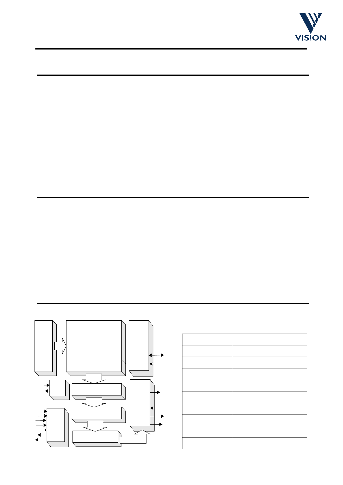
BLOCK DIAGRAM
SAMPLE & HOLD
HORIZONTAL SHIFT REGISTER
PHOTO DIODE ARRAY
ANALOG
VOLTAGE
REFS.
DIGITAL
CONTROL
LOGIC
SDA
SCL
VBLTW
VRT
VCM
VREF2V5
VERTICAL
SHIFT
REGISTER
CLKI
CLKO
CLOCK
CIRCUIT
IMAGE
FORMAT
Pixel Resolution 160 x 120
Pixel Size 12µm x 12µm
Array Size 1.92mm x 1.44mm
Power Supply 5v +/-10%
Min.illumination 5 Lux
Power 175 mW (Typ.)
S/N 36 dB (Typ.)
Exposure control Automatic (25000:1)
Temperature -20
o
C to +70oC
Package Ceramic 48LCC
A/D CONVERTOR
VPED
VCDS
D[7:0]
SIN
FST
QCK
VBG
Page 2

cd34021-a.fm 15/01/98 2
VV6300 Sensor
Main Features
Bayer pattern colour array with default image format of 160 x 120. Extra border pixel/lines can be enabled to
give an image size of 164 x 124. Shuffled read out to reduce pixel crosstalk. Digital pixel data coding assigns
10
H
as black and F0H as white. Other codes specify line sync and frame sync periods.
On-chip 8-bit successive approximation analogue-to-digital convertor with 8-wire, 4-wire parallel and two
serial data output modes.
The VV6300 frame rates can be integer multiples of the mains supply frequencies used worldwide, i.e. 50Hz
and 60Hz. This ensures reduced flicker operation of the sensor
All VV6300 operating modes and system status information can be accessed via a two wire bidirectional
serial interface.
VV6300 features an automatic electronic exposure algorithm that enables the use of a single fixed-aperture
lens. Automatic gain control enhances operation under low light conditions.
Automatic black level control ensures consistent picture quality across the whole range of operating
conditions. Extensive use of automated operation and on chip references means that only a small number of
passive components are needed to realise a complete video camera.
On-chip voltage references simplifies the support circuitry and maintains device stability over a wide range
of operating conditions.
Exposure Control
With automatic exposure control selected VV6300 uses a complex algorithm to automatically set the
exposure value for the current s cene. When combin ed with clock cont rol and gain con trol the VV6300 ca n
operate over a very wide range of illumination levels.
Where direct control of the exposure is required the exposure value can be directly selected by writing to the
appropriate registers via the serial interface.
Clock Control
The system clock can be divided down internally to extend the operating range of VV6300 by allowing longer
exposure times. The clock divisor can be varied from 1 to 8 in times two steps i.e there are 4 different values.
Note: changing the system clock divisor modifies the pixel and frame rate.
Gain Control
If the image is to dark an d the expo sure is al ready clo se to its ma ximum, V V6300 wil l increase th e system
gain.
Gain can be varied from x1 to x8 in times two steps i.e there are 4 different gain settings. If the scene is too
dark and integration period has almost reached its maximum value the gain value is incremented by one step
(i.e. doubled). If the gain setting changes the exposure value is automatically set to half the maximum
integration period. The exposure controller then increases the exposure value as necessary.
Similarly if the image is too bright and the i ntegrati on period is short then gain will be r educed by one ste p
(i.e. divide by two). As before, the exposure value is set to half the maximum integration period. The exposure
controller can then adjust the exposure value as necessary to provide a correctly exposed image.
Page 3
cd34021-a.fm 15/01/98 3
VV6300 Sensor
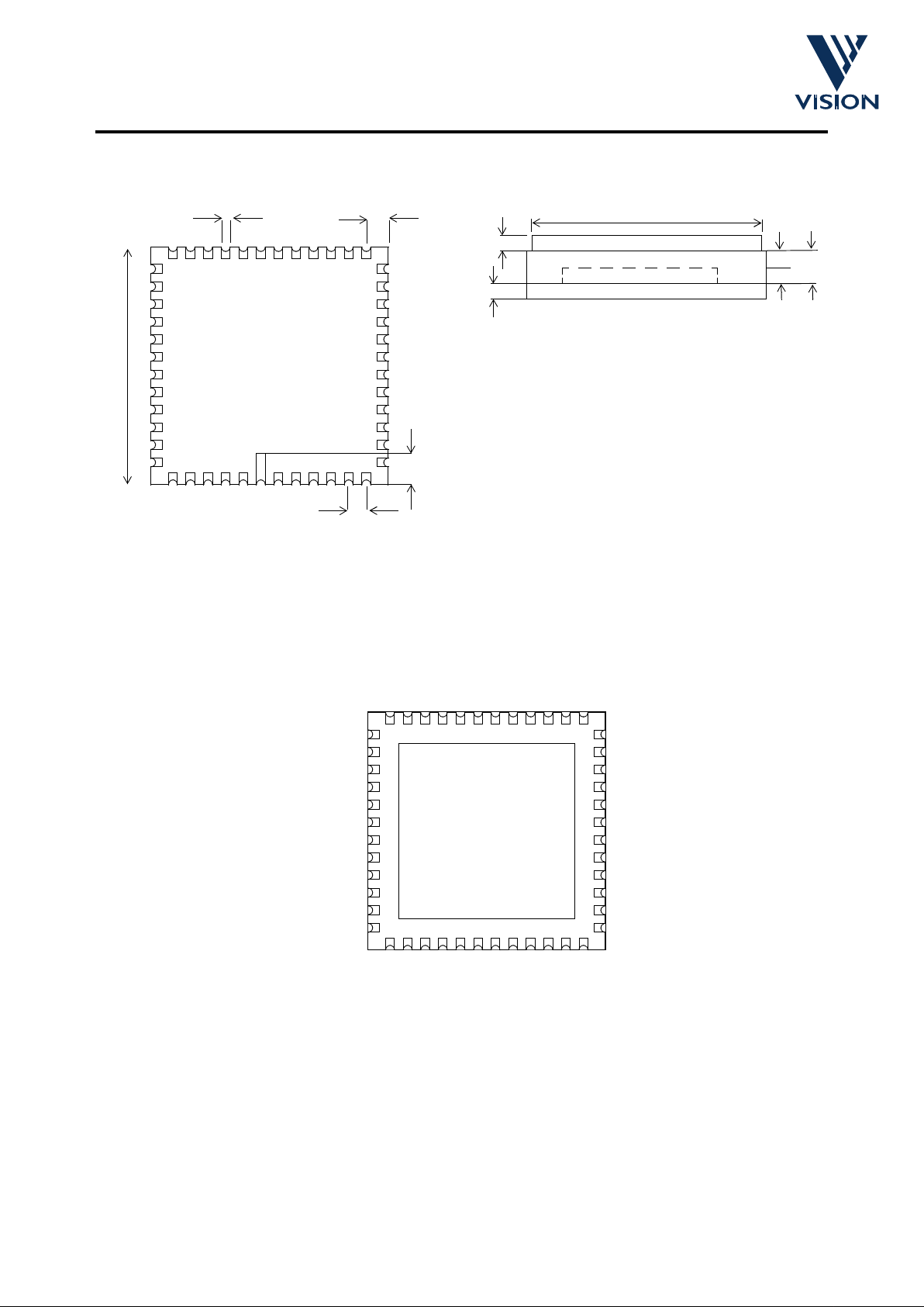
Package Details
Device Pinout
0.51
1.56
2.16
PIN 1
1.016 PITCH
14.22+/-2%
Viewed from below
0.53
0.55
Glass Lid
Base
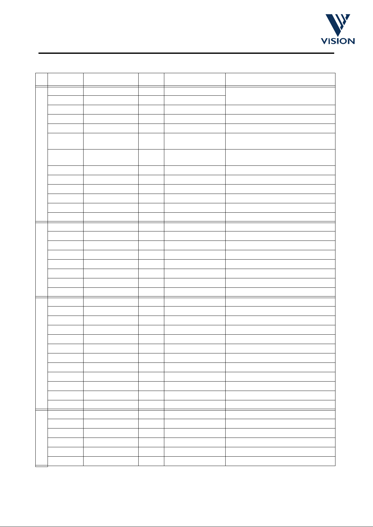
Viewed from side
Die
0.86
0.5
13.7
The optical array is centred within the
package to a tolerance of ± 0.2 mm, and
rotated no more than ± 0.5
o
Tolerances on package dimensions ±10%
unless otherwise stated.
Glass lid placement is controlled so that no
package overhang exists.
All dimensions in millimetres
12345643 44 45 46 47 48
18 NC
17 QCK
16 FST
15 SIN
14 VDD
13 DVDD
12
11
10
9
8
7
24 23 22 21 20 1930 29 28 27 26 25
31
32
33
34
35
36
37
38
39
40
41
42
VRT
VCDS
TEST
HPIX
NC
AVSS
NC
NC
NC
AVDD
NC
NC
VDD
VSS
D[7]
D[6]
D[5]
D[4]
D[3]
D[2]
D[1]
D[0]
VSS
VDD
CLKI
CLKO
SDA
SCL
VSS
DVSS
AUTOLOADB
CE
NC
VREG
NC
NC
NC
VBLOOM
VBLTW
VBG
VREF2V7
NC
VV6300
Viewed from above
Page 4
cd34021-a.fm 15/01/98 4
VV6300 Sensor
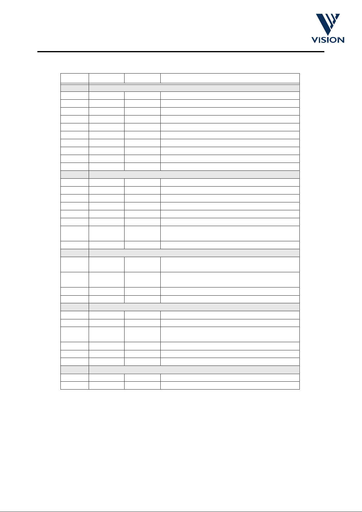
Pin Function List
OA - Analogue output A - Analogue input
OD - Digital output D - Digital input
BI - Bidirectional ID↑ − Digital input with internal pull-up
OD↓ − Digital output with internal pull-down
Pin Name Type Description
POWER SUPPLIES
6 AVSS GND Analogue ground
9 AVDD PWR Analogue power
13 DVDD PWR Digital power
14 VDD PWR Power
19 VDD PWR Power
20 VSS GND Ground
29 VSS GND Ground
30 VDD PWR Power
35 VSS GND Ground
36 DVSS GND Ground
ANALOGUE OUTPUTS
1 VRT IA Pixel reset voltage
2 VCDS IA Voltage reference
3 TEST IA Analogue test
40 VREG ΙΑ Reference voltage input
44 VBLOOM ΟΑ Internal reference voltage
45 VBLTW IA Bitline test white reference
46 VBG OA Internally generated bangap reference voltage
1.22V
47 VREF2V5 ΟΑ Internally generated reference voltage 2.5V
DIGITAL OUTPUTS
16 FST OD Frame start. Synchronises external image
capture.
17 QCK OD Pixel sample clock. Qualifies video output for
external image capture.
25-28 D[3:0] BI↓ Parallel 4-bit databus. D[0] seri al data bus.
21-24 D[7:4] OD↓ Parallel 4-bit databus.
DIGITAL CONTROL SIGNALS
34 SCL BI↑ Serial bus clock (bidirectional, open drain)
33 SDA BI↑ Serial bus data (bidirectional, open drain)
37 AUTOLO
ADB
ID↓ Enable autoload from EEPROM
38 CE ID↑ Chip enable
4HPIXID↓Hold pixel value.
15 SIN ID↓ Frame Timing reset(Soft reset)
SYSTEM CLOCKS
31 CLKI ID Oscillator input.
32 CLKO OD Oscillator output.
Page 5
cd34021-a.fm 15/01/98 5
VV6300 Sensor
SPECIFICATIONS
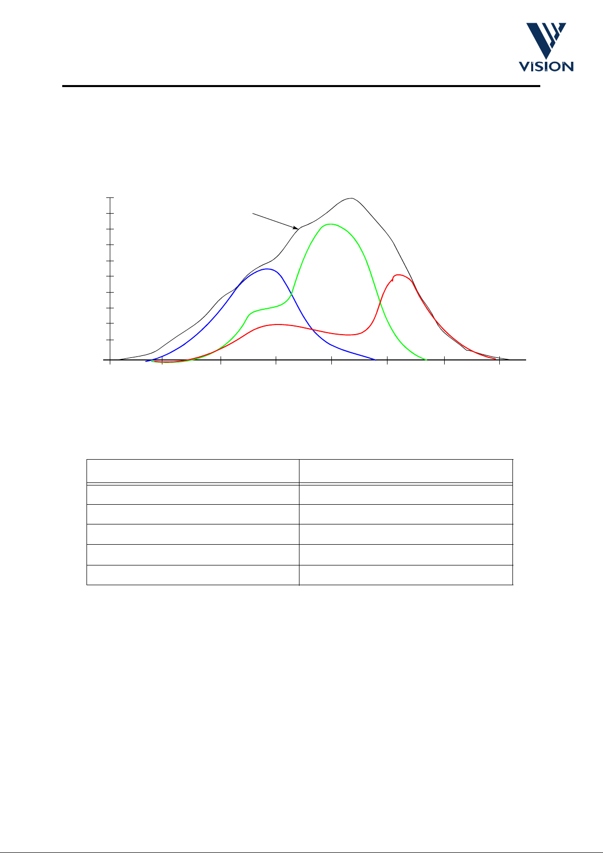
Spectral Response
Absolute Maximum Ratings
Note: Stresses exceeding the Absolute Maximum Ratings may induce failure. Exposure to absolute
maximum ratings for extended periods may reduce reliability. Functionality at or above these
conditions is not implied.
Parameter Value
Supply Voltage -0.5 to +7.0 volts
Voltage on other input pins -0.5 to V
DD
+ 0.5 volts
Temperature under bias -15
o
C to 85oC
Storage Temperature -30
o
C to 125oC
Maximum DC TTL output Current Magnitude 10mA (per o/p, one at a time, 1sec. duration)
400
500
600
700
Red
Green
Blue
1.0
0.8
0.6
0.4
0.2
0
with IR Filter
Sensor Response
Wavelength, nm
350
450
550
650
COLOURISATION
FILTER RESPONSES
Normalised Response
Page 6
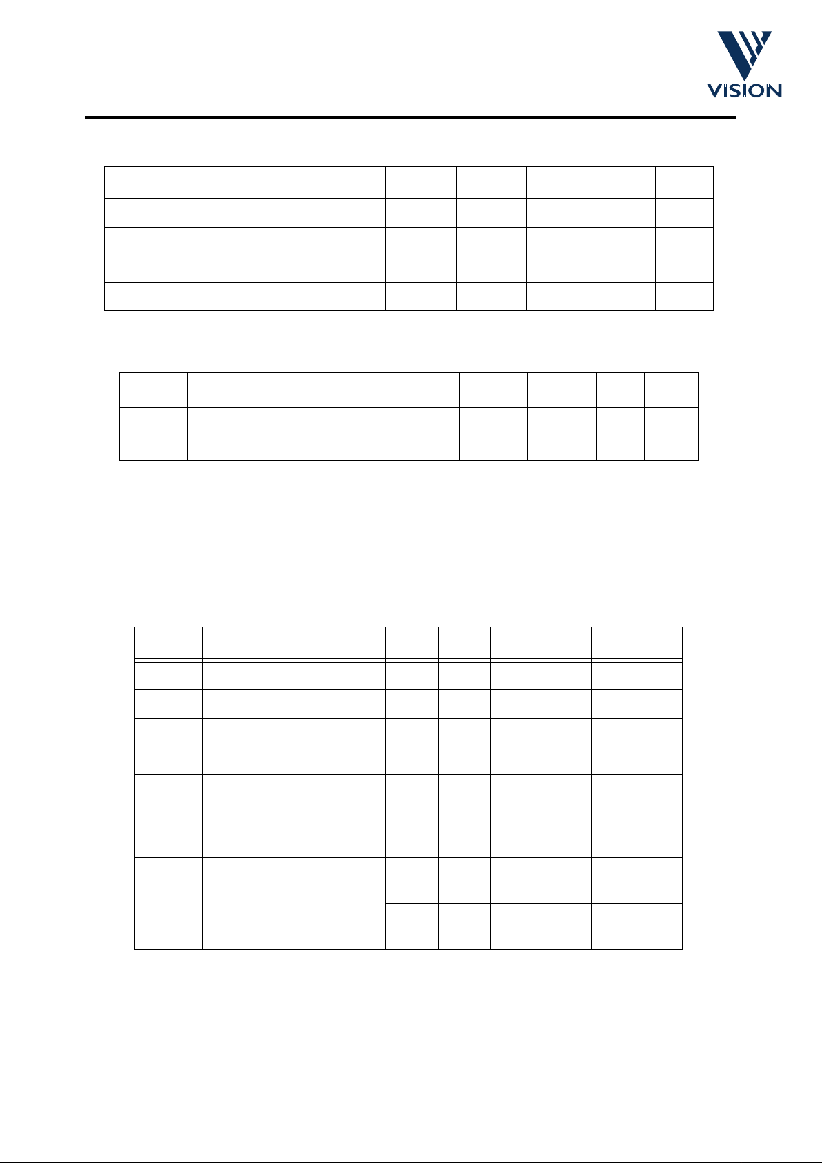
cd34021-a.fm 15/01/98 6
VV6300 Sensor
DC Operating Conditions
AC Operating Conditions
1. Pixel Clock =
CKIN
/
2
2. Serial Interface clock must be generated by host processor.
Electrical Characteristics
1. Digital and Analogue outputs unloaded - add output current.
Symbol Parameter Min. Typ. Max. Units Notes
V
DD
Operating supply voltage 4.75 5.0 5.25 Volts
V
IH
Input Voltage Logic “1” 2.4 VDD+0.5 Volts
V
IL
Input Voltage Logic “0” -0.5 0.8 Volts
T
A
Ambient Operating Temperature -20 70
o
C Still air
Symbol Parameter Min. Typ. Max. Units Notes
CKIN
Crystal frequency 14.318 MHz 1
SCL
Serial Data Clock 100 KHz 2
Symbol Parameter Min. Typ. Max. Units Notes
I
DCC
Digital supply current
10 mA 1
I
ADD
Analog supply current
25 mA 1
I
DD
Overall supply current
35 mA 1
V
REF2V7
Internal voltage reference 2.700 Volts
V
BG
Internal bandgap reference 1.22 Volts
V
OH
Output Voltage Logic “1” 2.4 Volts I
OH
= 2mA
V
OL
Output Voltage Logic “0” 0.6 Volts I
OL
= -2mA
I
ILK
Input Leakage current
-1 µA
VIH on
input
1 µA
VIL on
input
Typical conditions, V
DD
= 5.0 V, TA = 27oC
Page 7
cd34021-a.fm 15/01/98 7
VV6300 Sensor
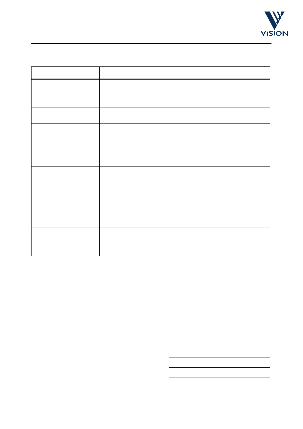
Operating Characteristics
Note: Devices are normally not 100% tested for the above characterisation parameters, other than
Dark Current Signal (see Blemish Specification below).
All voltage (VA, V
ave
, V
sat
, V
xx%
) measurements are referenced to the black lev el, V
black
, and spot
blemishes are excluded (see Blemish Specific ation below). V
xx%
refers to the output that is xx% of
saturation, that is peak white
T
est Conditions
Parameter min. typ. max. units Note
Dark Current Signal 50 mV/Sec Modal pixel voltage due to photodiode leak-
age under zero illumination with Gain=1
(V
dark
= (Vt1 - Vt2)/(t1-t2), calculated over
two different frames
Sensitivity 6 V/Lux·Sec V
Ave
/Lux·10ms, where Lux gives 50% satu-
ration with Gain=1 and Exposure=10ms
Min. Illumination 10 Lux
Shading TBA % Variance of V
ave
over eight equal blocks at
66% saturation level illumination
Random Noise -36 dB RMS variance of all pixels, at 66% satura-
tion, over four frames
Smear TBA % Ratio of V
ave
of the area outside a rectangle
25 lines high illuminated at 500xV
50%
level
to V
Ave
of the rectangle
Flicker TBA % Variation of V
ave
of one line from field to field
at 66% saturation level illumination
Lag TBA % Average residual signal with no illumination
in the field following one field of 66% sat.
illumination
Blooming TBA Ratio of spot illumination level that produces
0.1xV
sat
output from immediat ely around the
spot to the V
sat
spot illumination level (pin-
hole target)
The sensor is tested using the example support
circuit illustrated later in this document. Standard
imaging conditions used for optical test s employ a
tungsten halogen lamp to uniformly illumina te the
sensor (to better than 0.5%), or to illumina te
specific areas. A neutral density filter is used to
control the level of illumination where required.
Illumination Colour Temp. 3200o K
Clock Frequency 14.318MHz
Exposure Maximum
Gain x1
Auto. Gain Control (AGC) Off
Page 8
cd34021-a.fm 15/01/98 8
VV6300 Sensor
Blemish Specification
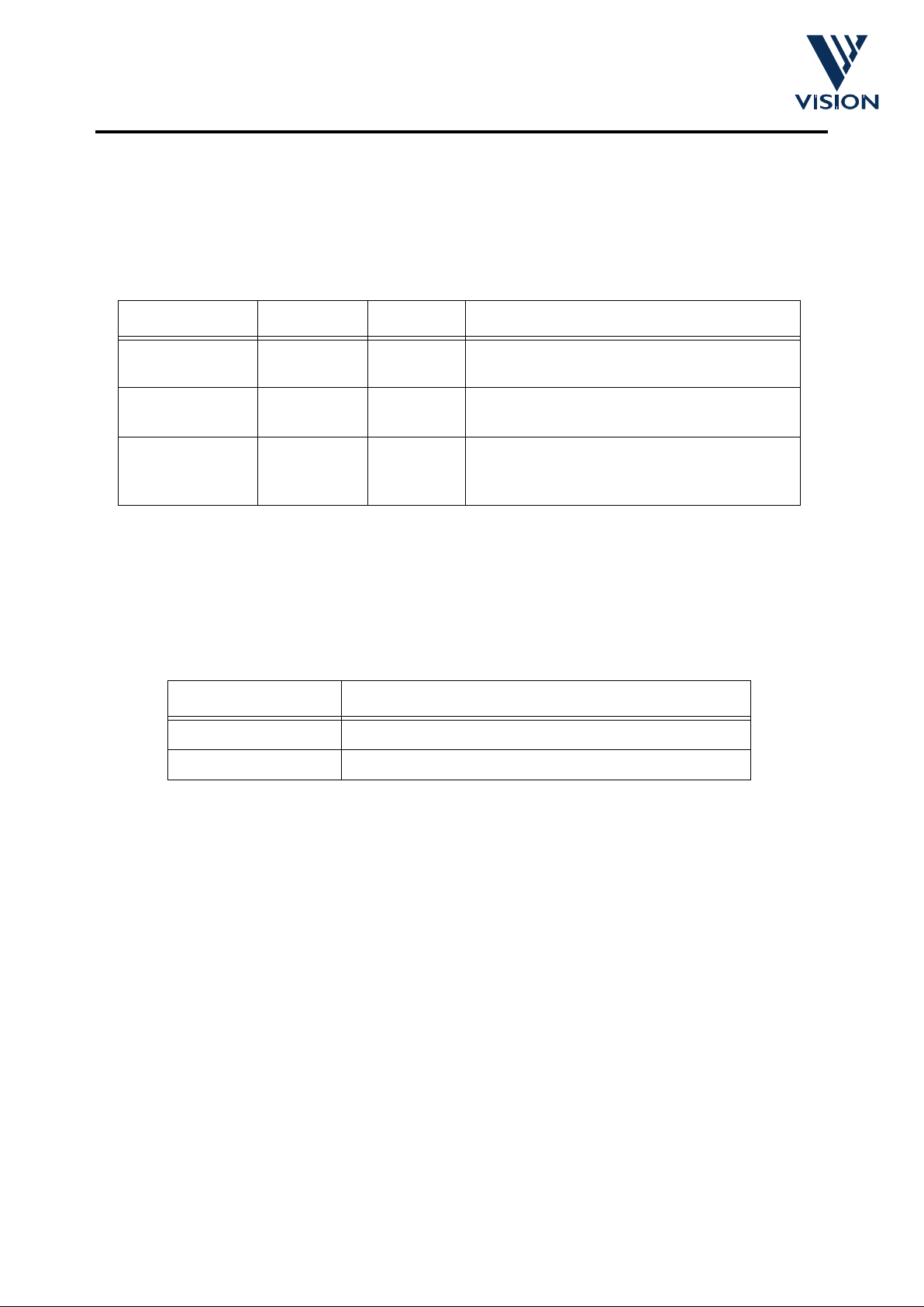
A Blemish is an area of pixels that produces output signifi cantly different from its surrounding pixels
for the same illumination level. The definition of a Blemish Pixel varies according to testing conditions as follows:
Note: Gain is set to Minimum and Correction set to Linear for all tests; measurement of blemishes for
Test 3 is conducted under standard illumination (see above), set to produce average output of
66% saturation level.
The blemish specification is then defined as foll o ws:
NB, pixel blemishes may occur anywhere on the array.
Test Exposure Illumination Blemish Pixel output definition
1 - Black Frame Minimum Black Differing more than ± 100 mV. from modal
value.
2 - Dark Current Maximum Black Output more than three times the modal value
(see Dark Current Signal above).
3 - Pixel Variation Mid range 66% Sat. Differing more than ±35mV from modal value.
Note: The mode of pixel values must be within
±70 mV of 66% of V
sat
for all devices.
Max. No. of Blemishes Notes
4 Unconnected single pixels
1 Of up to four connected pixels (2x2 max.)
Page 9
cd34021-a.fm 15/01/98 9
VV6300 Sensor
System Clock Generation
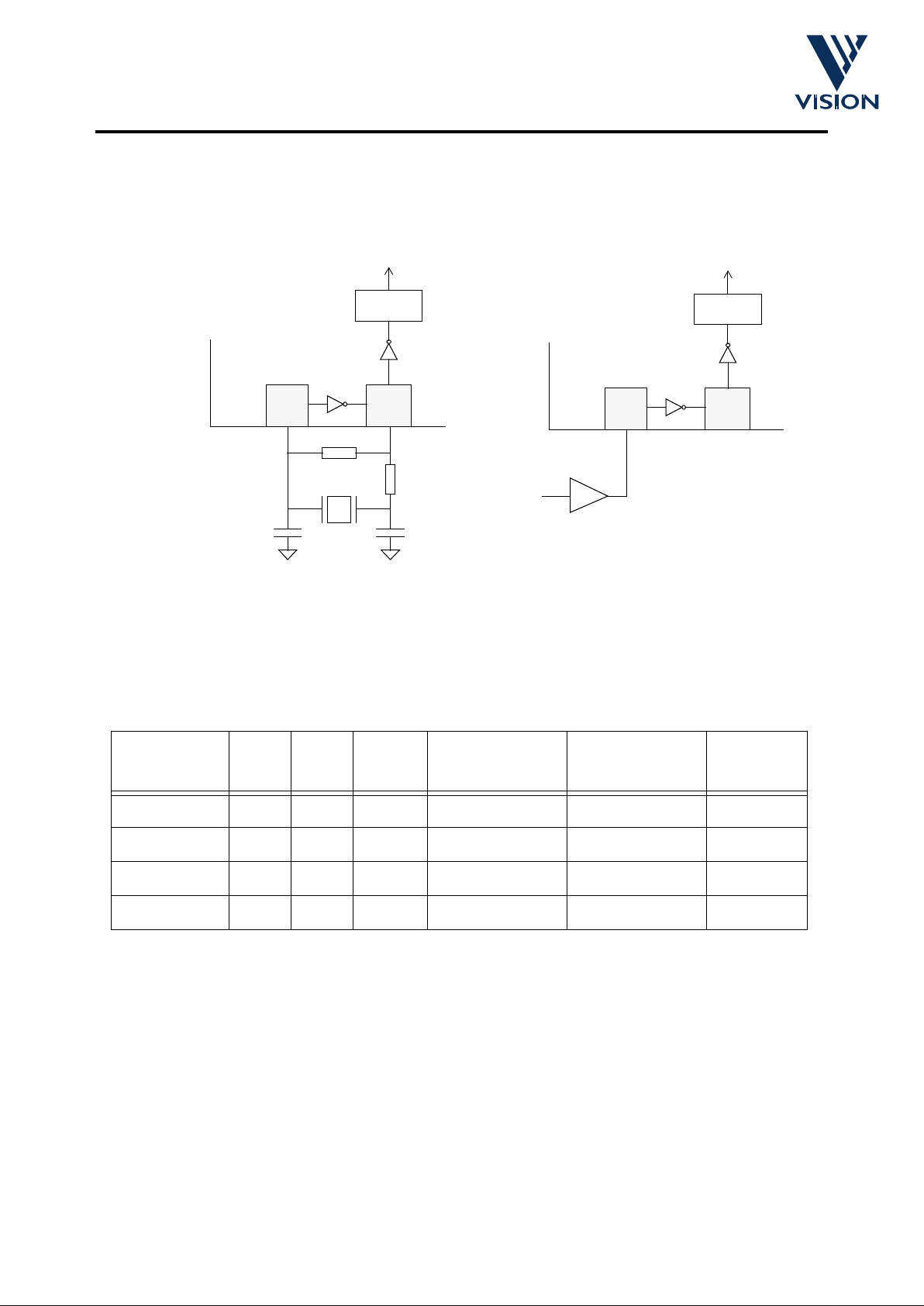
VV6300 generates a system clock when a quartz crystal or ceramic resonator circuit is connected to the CLKI
and CLKO pins. The device can also be driven directly from an external clock source driving CLKI.
Camera Clock Source
For greater flexibility the input frequency can be divided by 1, 2, 4 or 8 to select the pixel clock frequency.
Two bits in the clock division register in the serial interface select the input clock frequency divisor. The table
below gives the different frame rates that can be selected, when CLKI = 14.318MHz, for each divisor. The
default clock divisor setting is a divide by 2. To achieve maximum frame rates data is converted at 4 bit
resolution.
CLKI
(MHz)
Divisor
Pixel Freq.
(kHz)
Frame rate
1
(fps)
1. Approximate frame rate. Assumes 160 x 120 image format, parallel data output and 4 bit data
conversion
Comments
14.318 0 0 1 1790 59.98 default
14.318 0 1 2 895 29.99
14.318 1 0 4 448 15.01
14.318 1 1 8 224 7.5
Clock Division (60Hz Video Mode)
X1
C2
C1
R1
32 31
CKIN
CKOUT
CLK
VV6300
3231
CKIN
CKOUT
VV6300
CMOS Driver
Clock
Source
R2
C1=C2=47pF
R1=1MΩ
R2=510Ω
X1= 14.318MHz (up to 60fps)
17.73MHz (up to 50fps)
CLOCK
DIVISION
CLK
CLOCK
DIVISION
Page 10
cd34021-a.fm 15/01/98 10
VV6300 Sensor
Image Format
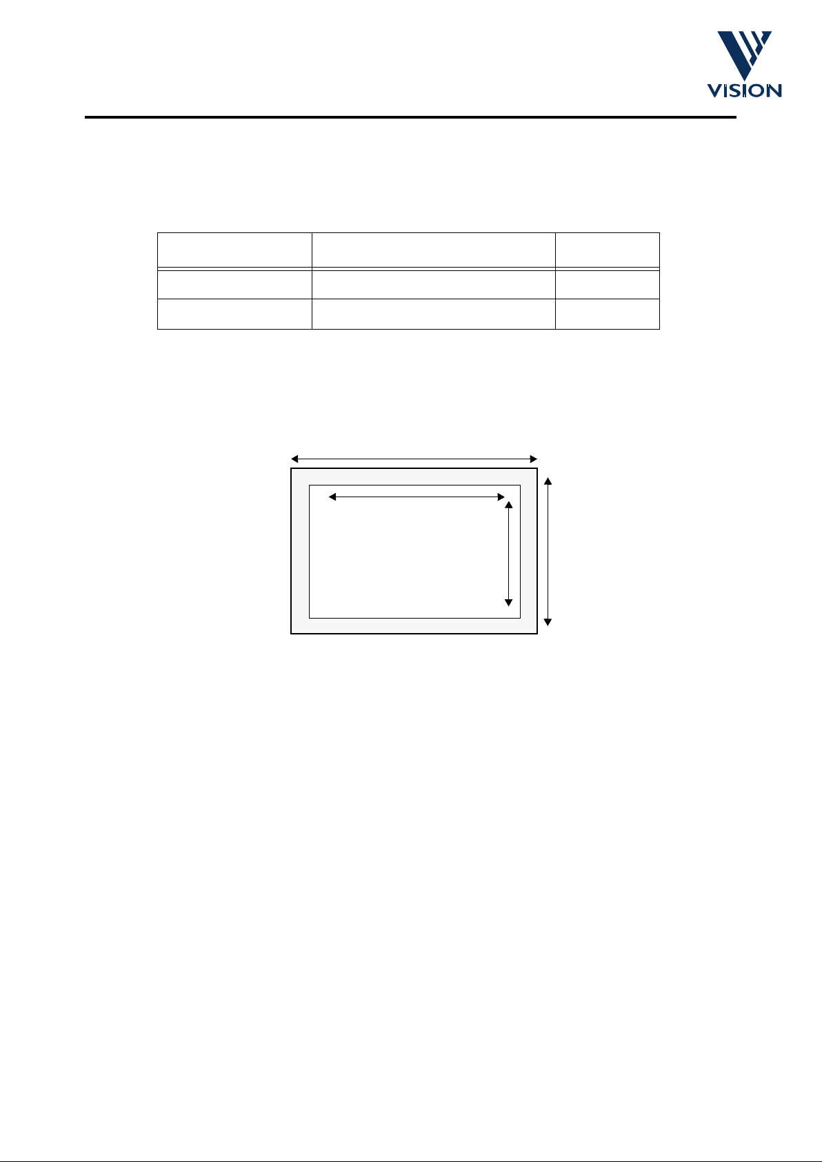
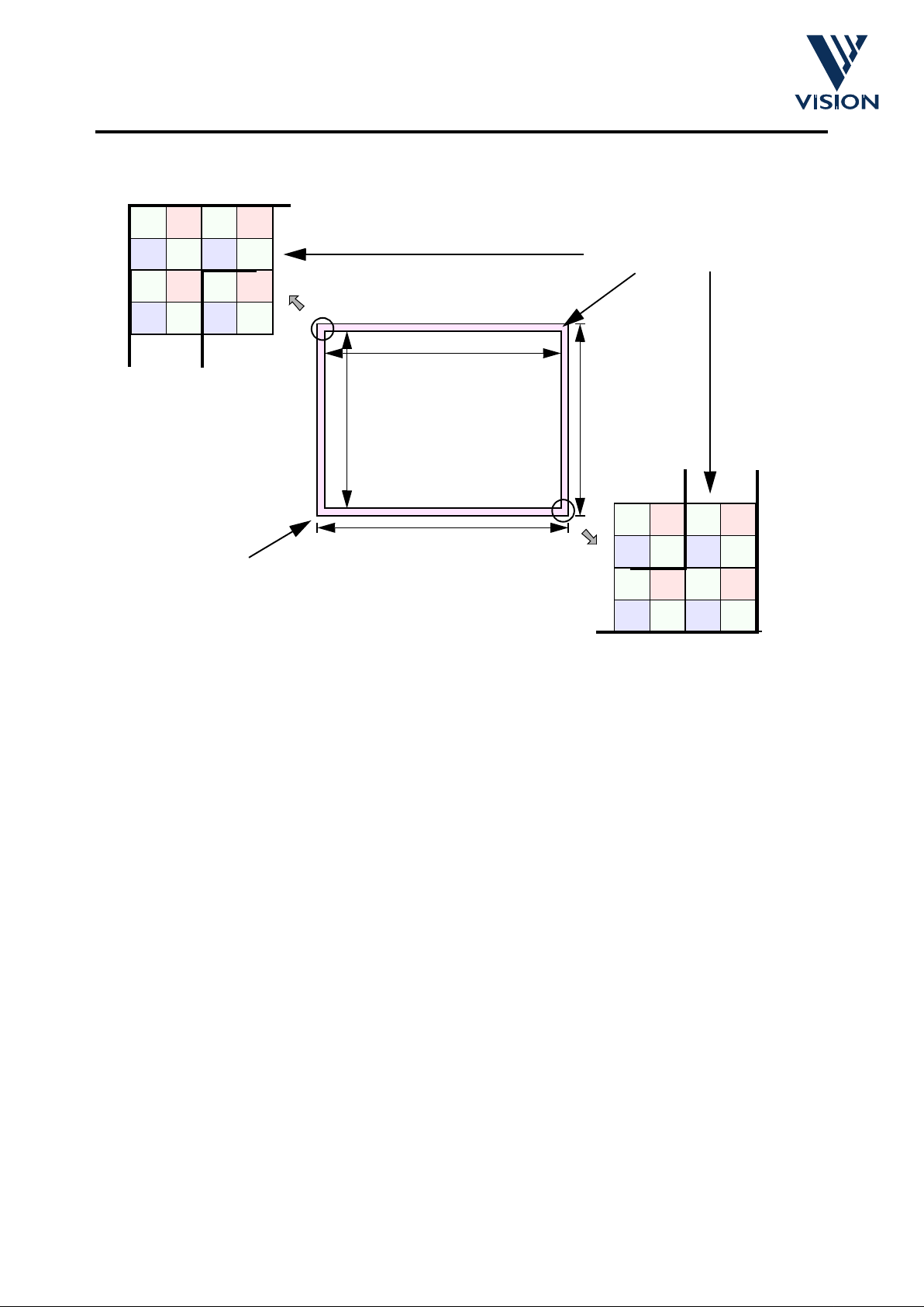
VV6300 has a single output image size, 160 x 120 pixel. The image size can be modified by asserting the
“enable borders” serial interface register bit, (Setup1, [001_0001
2
]). The extended image size is 164 x 124
pixels. The default image format is 160 pixels by 120 lines.
Image Format Selection
The diagram below shows the relationship between the default 160 x 120 pixel image and the extended 164
x 124 pixel format. A border, 2 pixels wide is enabled around the basic array.
Output Image Dimensions
Enable borders Image size (column x row) Comment
0 160 x 120 default
1 164 x 124
164
124
160
120
Page 11

cd34021-a.fm 15/01/98 11
VV6300 Sensor
Frame Timing
The VV6300 frame rate depends upon:
(i) the frequency of the system clock (CLKI)
(ii) the ADC conversion accuracy (8-bit or 4-bit)
(iii) the internal clock divisor selected (1, 2, 4, or 8)
(iv) the output format selected (8-wire, 4-wire, serial or UART)
User can set their own values for CLKI, the ADC conversion rate and also the clock divisor setting, subject
to achieving a frame rate up to 60 frames/sec.
The frame rate is determined in the following way:
An example is given with a clock input of 14.318MHz, 160 x120 image format, 8-bit ADC conversion rate and
a clock divisor of 2.
1. Determine clock input (CLKI) frequency - 14.318MHz
2. Pixel period = (divisor x conversion factor x output format factor) / CLKI
Clock divisor = 1, 2, 4 or 8.
Conversion factor = 8 for 8-bit ADC accuracy
= 4 for 4-bit ADC accuracy
Output format factor = 2 for 8-wire, 4-wire, serial output modes
= 6 for UART mode
Example: Pixel period = (2 x 8 x 2) / 14.318MHz= 2.235µs
3. Line period = (no. of visible pixels + line overhead) x pixel period
The number of visible pixels per line is 160. The interline pixel period overhead (including the 4 border pixels
that can be enabled t o qualify extra v ideo i nformati on) is m ode dep endent, 4 3 pix el perio ds for 60Hz mode
or 141 pixel periods for 50Hz mode.
Example: Line period = (160 + 43) x 2.235µs= 453.705µs
4. Frame period = (no. of visible lines + frame overhead) x line period
For the purposes of calculat ing the e ffec ti ve frame r ate the n umb er of ac tive li nes is assumed to be fixed at
120. The frame overhead (which includes the 4 border lines that can be enabled to qualify extra video
information) has a constant value of 27 line periods.
Example: Frame period = (120 + 27) x 453.705µs= 66.694ms
Frame rate = 1 / frame period = 15 frames per second
Page 12
cd34021-a.fm 15/01/98 12
VV6300 Sensor
Digital Data Output Modes
VV6300 provides several different output modes. The different data formats are selected via the appropriate
register in the serial interface, Setup0, [001_0000
2
], bits 5 and 6. 8-bit or 4-bit pixel data conversion is also
selected via the serial interface, Setup1, [001_0001
2
]. If 4-bit pixel data conversion is selected as well as 8Wire parallel output format then 2 consecutive pixel nibbles may be packed into a single output byte therefore
increasing the effective frame rate.
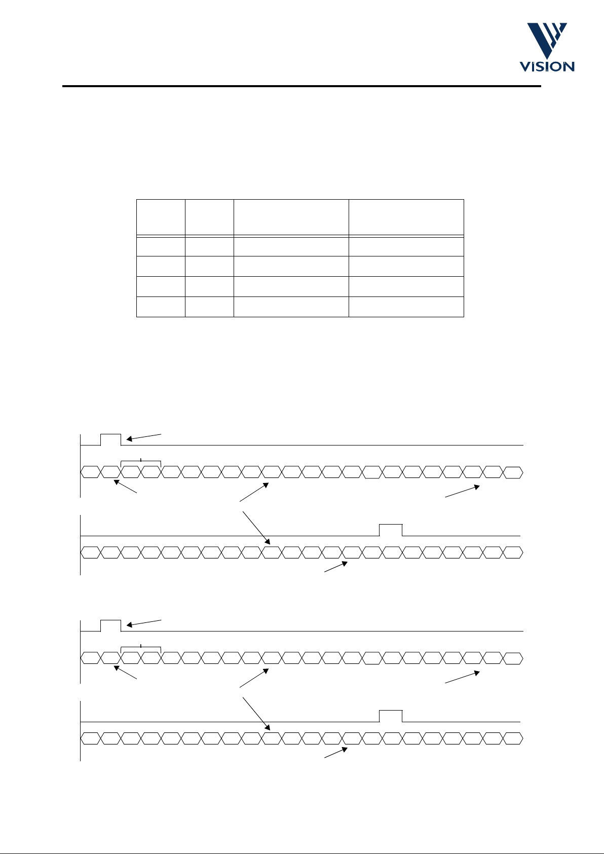
Frame Level Formatting
The frame level format for each mode is common and is given below. FST can be used for frame
synchronisation. The FST pulse is exactly one line period in length and the rising edge occurs just before the
status line start sequence (see line level formatting) is output.
Frame Format (160 x 120 mode)
Frame Format (164 x 124 mode)
Setup
Bit 6
Setup
Bit 5
Description Comment
0 0 8-Wire Parallel
0 1 4-Wire Parallel default
10 Serial
11 Serial UART
Data Output Modes
BL
Line
FST
BL ST BK BK BL
BL BL BL BL
BL BL
BLBLBL BL BL BL BL
BL FE BL ST
BL BL
BL
VL BL
BL
BL BL
BL
BL VL VL VL VL VL VL VL
BL BL
Line
FST
Black Lines (BK)
Blank Lines (BL)
Visible Lines (VL)
Start / Status Line (ST)
120 Visible Lines
Frame Start
BL
Frame End (FE)
Frame Period = 147 Lines
VL
BL
Line
FST
BL ST BK BK BL
BL BL BL BL
BL BL
BLBLBL BL BL BL BL
BL FE BL ST
BL BL
BL
VL VL
VL
BL BL
BL
VL VL VL VL VL VL VL VL
BL BL
Line
FST
Black Lines (BK)
Blank Lines (BL)
Visible Lines (VL)
Start / Status Line (ST)
124 Visible Lines
Frame Start
VL
Frame End (FE)
Frame Period = 147 Lines
VL
Page 13

cd34021-a.fm 15/01/98 13
VV6300 Sensor
Line Level Formatting
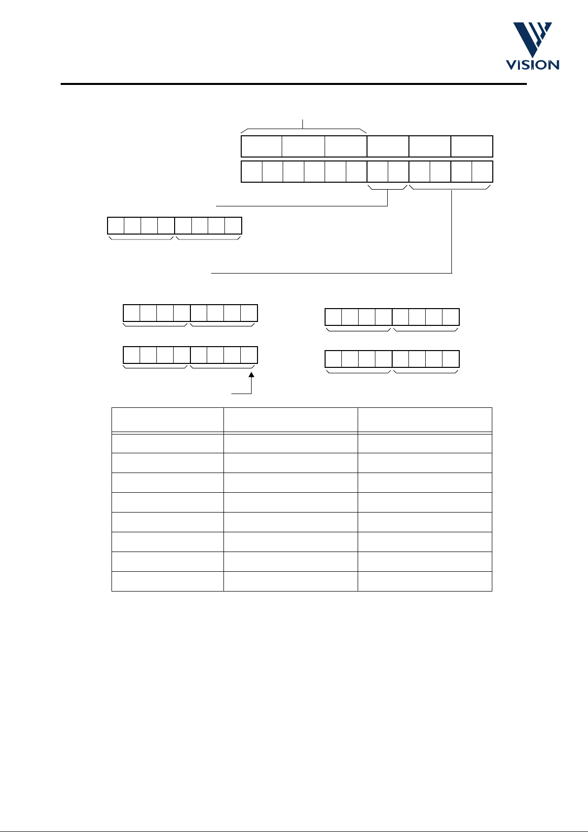
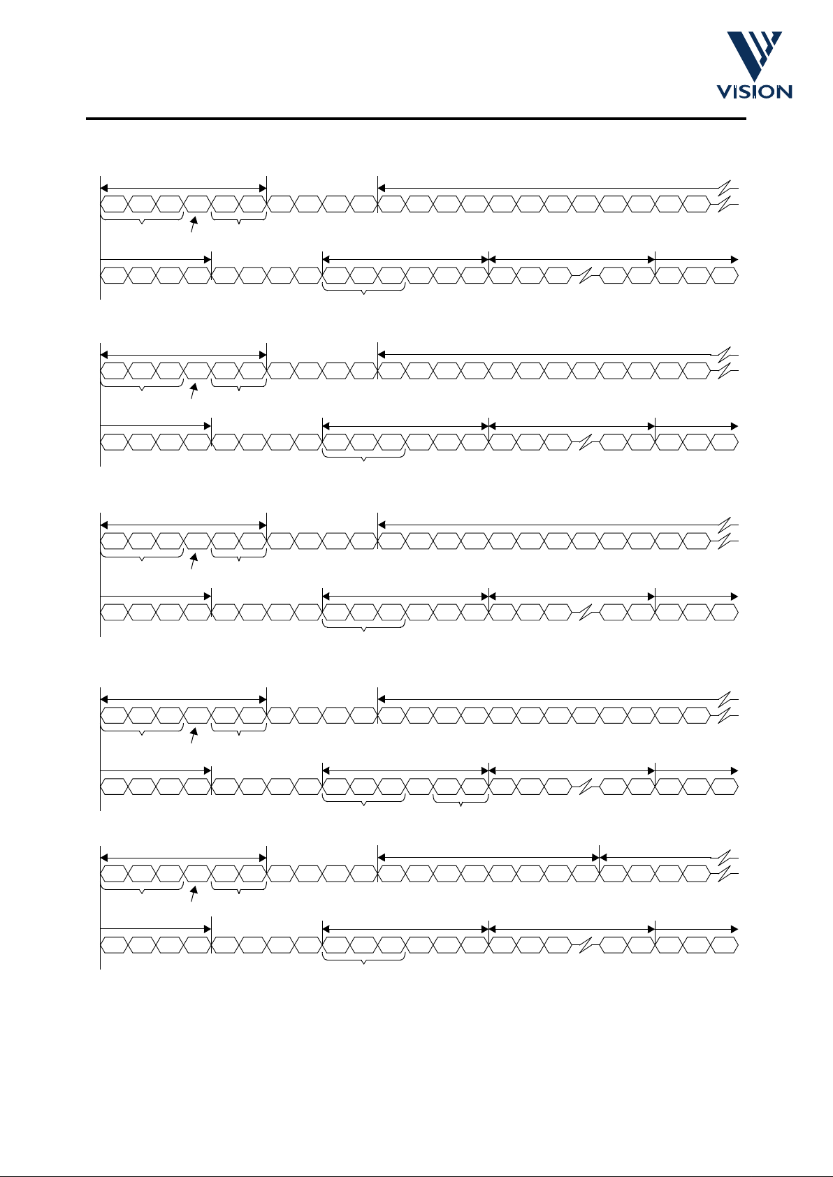
Each line type (black, blank, visible) has a specific format associated with it independent of the data output
format selected. Each line begins with a start sequence of FF
H
FFH 00H followed by XYH where XYH indicates
the line type. The next two bytes provide supplementary data (specifically the line number within the current
frame). Following this data are two guaranteed blank bytes (07
H 07H
for 8 bit modes, 01H01H for 4 bit modes).
If the border lines/pixels have been enabled the next 2 bytes will be visible pixels otherwise they shall appear
as blank bytes. The next part of the line is reserved for the 160 visible pixels. The 4 bytes following the visible
pixels are formatted in the same way as the 4 bytes preceeding the 160 visible pixels. At the end of each line,
an end of line sequence is produced, (FF
H
FFH 00H 80H). If the line is within the visible part of the frame,
(lines 11 to 134 if the border lines are enabled otherwise lines 13 to 132), the end of line sequence is
immediately followed by 2 bytes containing the mean values for the central 128 pixels. The first byte contains
the mean value for the first 64 pixels of the middle 128 pixels and the second byte contains the mean value
for the latter 64 pixels of the middle 128 pixels. The 128 pixels comprise the standard 120 visible pixels, the
4 border pixels and an extra 4 border pixels that are never enabled as visible pixels but are used for exposure
control and hence contribute to the mean pixel value for the line. If the line type is not visible then the two
bytes following the end of line sequence will contain 07
H
07H. For the remainder of the interline period the
data output is always FF
H
.
Sensor status and configuration information is output during the frame start line, (line 0), each data byte is
separated by a blank value (07
H
) to avoid possible false line start conditions being generated. The
information output during the status line reflects, if the sensor is operating in 8bit ADC mode, the first 64
locations in the serial interface register map. If the sensor is operating in 4 bit mode less data can be output
during the status line. All the serial interface registers are 8bit values therefore 2, 4bit pixel periods are
required to output a single serial interface location. Note that the serial interface data is only output during
the visible monochrome pixels of the status line. This allows for one quarter of the serial interface address
space to be output during any status line. It is possible to select the remaining registers in the serial interface
for output, (see serial interface register setup 2, bits 7:6).
The “end of frame” line, it is actually 2 lines prior to the status line will output the 4 exposure control bin
averages during the first 4, (or 8 if operating in 4bit modes) monochrome pixels. Again the data is separated
by mode dependent padding data.
Page 14
cd34021-a.fm 15/01/98 14
VV6300 Sensor
Line Code Nibble XH [1 C2 C1 C0]Nibble YH [P3P2P1P0]
End of Line 10002 (8H) 00002 (0H)
Blank Line (BL) 10012 (9H) 11012 (DH)
Black line (BK) 1010
2 (AH
) 10112 (BH)
Visible Line (VL) 1011
2 (BH
)0110
2
(6H)
Start of Frame (SOF) 11002 (CH) 01112 (7H)
End of Frame (EOF) 1101
2 (DH
) 10102 (AH)
Reserved 1110
2 (EH
) 11002 (CH)
Reserved 11112 (FH) 00012 (1H)
(i) Line Number (L11 MSB)
Odd word parity
or (ii) If Line Code = End of Line then
Mean Pixel Value for first half of the line
Mean Pixel Value for second half of the line
L
7
L
8
L6PL
11
0
L10L
9
L
1
L
2
L0PL
5
0
L4L
3
M
2
M
3
M1M
0
M
6
M
7
M5M
4
(Line Code)
Escape/Sync Sequence
F
H
F
H
F
H
F
H
0
H
0
H
Y
H
X
H
D
2
D
3
D
0
D
1
P
2
P
3
P1P
0
Nibble X
H
Nibble Y
H
C
2
1
C1C
0
Command
4-wire output mode
FF
H
FF
H
00
H
XY
H
D3D2D1D
0
8-wire output mode
Supplementary Data
Nibble D
3
Nibble D
2
Nibble D
1
Nibble D
0
N
2
N
3
N1N
0
N
6
N
7
N5N
4
Page 15
cd34021-a.fm 15/01/98 15
VV6300 Sensor
Line Coding
BLANK
BLACK
FRAME
VISIBLE
FFHFF
H
C7HLN 07H07
H
FF
H
00
H
FF
H
07
H
80
H
07H07
H
Sensor Status Data
FFHFFH00
H
07
H
07
H
LN
07
H
FRAME
SD 07HSD 07HSD 07HSD 07HSD 07
H
00
H
SD 07
H
SD 07HSD 07
H
FF
H
FF
H
FF
H
FF
H
Line Start Sequence
Line Start
Line Type
Line Number
FF
H
Line End Sequence
Line End
Next Line Start
Inter-Line Period
FFHFF
H
ABHLN 07H07
H
FF
H
00
H
FF
H
07
H
80
H
07H07
H
Black Level Pixel Values (Nominally - 10H)
FFHFFH00
H
LN
07
H
PV PV PV PV PV PV PV PV PV PV
00
H
PV PV
PV PV PV PV
FF
H
FF
H
FF
H
FF
H
Line Start Sequence
Line Start
Line Type
Line Number
FF
H
Line End Sequence
Line End
Next Line Start
Inter-Line Period
FFHFF
H
9DHLN 07H07
H
FF
H
00
H
FF
H
07
H
80
H
07H07
H
Blank Level (07H)
FFHFFH00
H
07H07
H
07H07
H
LN
07
H
07H07H07H07H07H07H07H07H07H07
H
00
H
07H07
H
07H07H07H07
H
FF
H
FF
H
FF
H
FF
H
Line Start Sequence
Line Start
Line Type
Line Number
FF
H
Line End Sequence
Line End
Next Line Start
Inter-Line Period
FFHFF
H
B6HLN 07H07
H
FF
H
00
H
FF
H
MN80
H
07H07
H
160 Visible Pixels
FFHFFH00
H
LN
MN
PV PV PV PV PV PV PV PV PV PV
00
H
PV PV
PV PV PV PV
FF
H
FF
H
FF
H
FF
H
Line Start Sequence
Line Start
Line Type
Line Number
FF
H
Line End Sequence
Line End
Next Line Start
Inter-Line Period
Black = 10H - White = F0
H
Line Mean Values
FFHFF
H
DAHLN 07H07
H
FF
H
00
H
FF
H
07
H
80
H
07H07
H
FFHFFH00
H
07H07
H
LN
07
H
MN
MN MN
07H07
H
00
H
07H07
H
07H07H07H07
H
FF
H
FF
H
FF
H
FF
H
Line Start Sequence
Line Start
Line Type
Line Number
FF
H
Line End Sequence
Line End
Next Line Start
Inter-Line Period
Frame Mean Values
END
START
07H07
H
07
H
07
H
07
H
07
H
07
H
07
H
07
H
07
H
MN07H07
H
07
H
07
H
07
H
07
H
Page 16
cd34021-a.fm 15/01/98 16
VV6300 Sensor
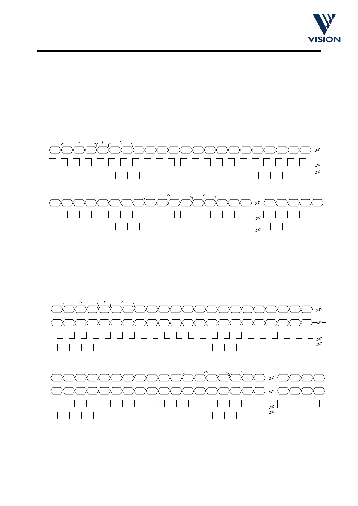
8-Wire Parallel Mode
8-Wire parallel mode is selected when the appropriate bits are set via the serial interface.
When 8-bit conversion mode is selected the 8-bit pixel data is output on pins DATA[7:0]. The start of a frame
is indicated by a pulse on FST. The data is valid on the falling edge of the pixel sample clock fast QCK (QCK
F
)
or on each edge of the slow QCK (QCK
S
).
8-Wire Parallel Mode (8-bit Pixel Data)
When 4-bit conversion mode is selected the 4-bit pixel data is output two bytes at a time on the DATA[7:0]
pins. The first pixel is mapped onto DATA[7:4] and the second pixel is output on DATA[3:0]. This effectively
doubles the pixel rate (and halves the frame period).
8-Wire Parallel Mode (4-bit Pixel Data)
DATA[7:0]
QCK
F
FF
H
FF
H
B6HLN 07H07
H
FF
H
00
H
FF
H
MN80
H
07H07
H
FFHFFH00
H
LN
MN
00
H
P117 P118 P119 P120
FF
H
FF
H
FF
H
FF
H
FF
H
DATA[7:0]
FF
H
Line Start Line No.Line Type
Line End
Line Mean
QCK
S
QCK
F
QCK
S
P0
P1 P2
P3 P4 P5
P6 P7 P8 P9 P10
07H07
H
07
H
07
H
DATA[7:4]
FHF
H
6HLN 1
H
0
H
F
H
MN8
H
1HFHFH0
H
P1
P118
LN
MN
P3 P5 P7 P9 P11 P13 P15 P17 P19 P210
H
P23
P110 P112 P114 P116 F
H
F
H
F
H
FHF
H
BHLN 1
H
P0LN P2 P4 P6 P8 P10 P12 P14 P16 P18 P200
H
P22
DATA[3:0]
0
H
F
H
MN0
H
1HFHFH0
H
P119 MNP111 P113 P115 P117 F
H
F
H
F
H
DATA[7:4]
DATA[3:0]
P104 P106 P108
P105 P107 P109
F
H
F
H
Line Start Line No.Line Type
Line End
Line Mean
QCK
F
QCK
S
QCK
F
QCK
S
P25
P24
P102
P103
1
H
1
H
1
H
1
H
Page 17
cd34021-a.fm 15/01/98 17
VV6300 Sensor
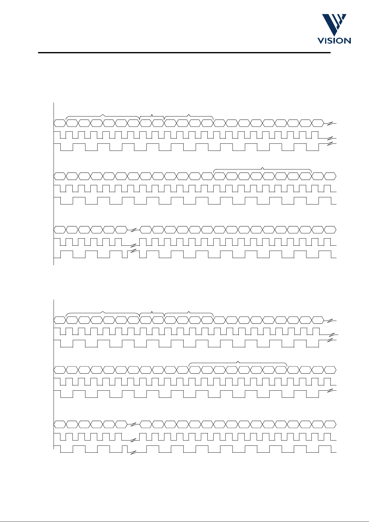
4-Wire Parallel Mode
4-Wire parallel mode is selected when the appropriate bits are set via the serial interface. When 8-bit data
conversion mode is selected (CONV8 = 1) the 8-bit pixel data is output on pins DATA[7:4] in two 4-bit nibbles.
The start of a frame is indicated by a pulse on FST. A QCK sample edge is generated for each nibble.
4-Wire Parallel Mode (8-bit Pixel Data)
When 4-bit data conversion mode is selected (CONV8 = 0) the 4-bit pixel data is output on pins DATA[7:4].
4-Wire Parallel Mode (4-bit Pixel Data)
DATA[7:4]
FHF
H
FH0
H
BH6
H
F
H
0H7
H
FHFHF
H
LN LN
0
H
MN
LN LN 0H7H0H7
H
F
H
P0
DATA[7:4]
0H7
H
0
H
8H0
H
0
H
MN
F
H
F
H
FHFHF
H
MN F
H
MN
FHF
H
P119P118P116 P117P115
FHF
H
FH0
H
BH6
H
LN LN
0
H
LN LN
F
H
F
H
Line Start Line No.Line Type
Line End
DATA[7:4]
QCK
F
QCK
S
QCK
F
QCK
S
QCK
F
QCK
S
0
H
7
H
7
H
0
H
0H7
H
7
H
0
H
DATA[7:4]
FHF
H
FH0
H
BH6
H
F
H
1H1
H
FHFHF
H
LN LN
0
H
MN
LN LN 1H1
H
P0 P1 P2 P3
F
H
P4
DATA[7:4]
0
H
8H0
H
0
H
MN
F
H
F
H
FHFHF
H
FHF
H
F
H
FHF
H
FHF
H
FH0
H
BH6
H
LN LN
0
H
LN LN
F
H
F
H
Line Start Line No.Line Type
Line End
DATA[7:4]
F
H
F
H
P119P118P117P116P115P114P113
QCK
S
QCK
F
QCK
S
QCK
F
QCK
S
QCK
F
1H1
H
1H1
H
Page 18
cd34021-a.fm 15/01/98 18
VV6300 Sensor
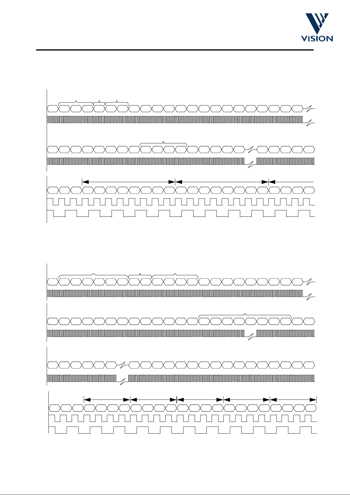
Serial Mode
Serial mode is selected when the appropriate bits are set via the serial interface. When 8-bit data conversion
mode is selected the 8-bit pixel data is output on pin DATA[0] least significant bit first.
Serial Mode (8-bit Pixel Data)
When 4-bit data conversion mode is selected (CONV8 = 0) the 4-bit pixel data is output on pin DATA[0] least
significant bit fi rst.
Serial Mode (4-bit Pixel Data)
0123
4
7
6
DATA[0]
Pixel_0
Pixel_1 Pixel_2
5
0123
4
7
6
5 0123
DATA[0]
QCK
FF
H
FF
H
B6HLN 07H07
H
FF
H
00
H
FF
H
MN80
H
07H07
H
FFHFFH00
H
LN
MN
P0 P1 P2 P3 P4 P5 P6 P7 P8 P9
00
H
P10
P116 P117 P118 P119
FF
H
FF
H
FF
H
FF
H
FF
H
DATA[0]
QCK
FF
H
Line Start
Line No.
Line Type
Line End
QCK
F
QCK
S
07H07
H
07
H
07
H
0
3
2
DATA[0]
Pixel_0
Pixel_1 Pixel_2
1
0
3
2
1
Pixel_3 Pixel_4
0321
0321
021
3
F
H
F
H
F
H
0
H
B
H
6
H
LN LN
0
H
LN LN 1H1
H
P2 P3
F
H
P4
F
H
F
H
1H1
H
FHFHF
H
MN
P119
0
H
8H0
H
0
H
MN
P117 P118P116P114 P115P113
F
H
F
H
FHFHF
H
FHF
H
F
H
FHF
H
FHF
H
FH0
H
BH6
H
LN LN
0
H
LN LN
F
H
DATA[0]
QCK
DATA[0]
QCK
DATA[0]
QCK
Line Start Line No.
Line Type
Line End
QCK
F
QCK
S
P5 P6
P112P111
1
H
1
H
1
H
1
H
Page 19
cd34021-a.fm 15/01/98 19
VV6300 Sensor
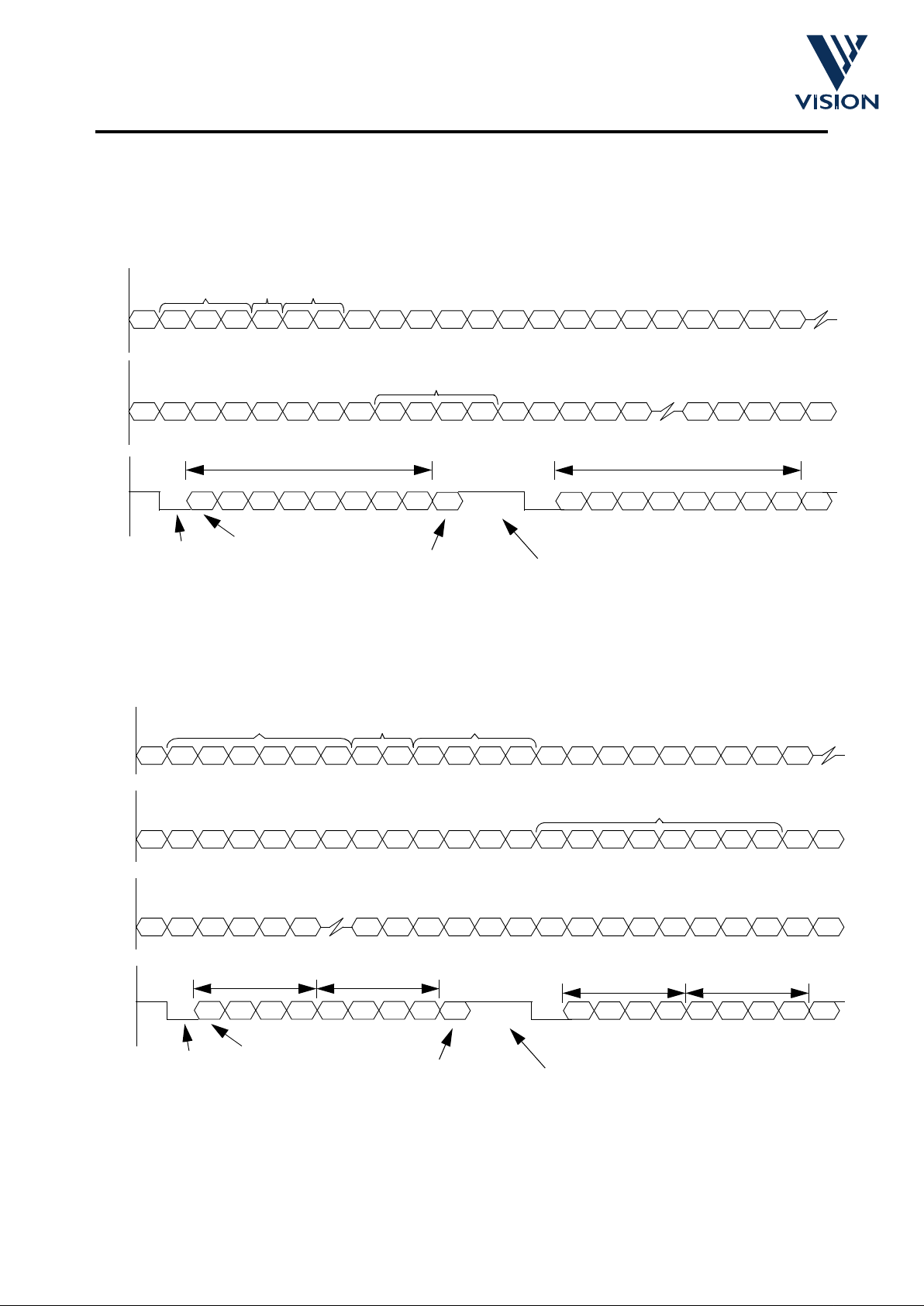
Serial UART Mode
Serial UART mode is selected when the appropriate bits are set via the serial interface. When 8-bit data
conversion mode is selected the 8-bit pixel data is output on pin DATA[0] least significant bit first. Each pixel
is preceded by a start bit and followed by an additional data bit and two stop bits.
Serial UART Mode (8-bit Pixel Data)
When 4-bit data conversion mode is selected the 4-bit pixel data is output two pixels at a time on pin DATA[0]
least significant bit first. Each pixel is preceded by a start bit and followed by an additional data bit and two
stop bits.
Serial UART Mode (4-bit Pixel Data)
All the above output format modes assume that the sensor is operating in the default sensor read-out mode,
namely, non shuffle and a monochrome image size of 160 by 120. The visible image can be increased to 164
by 124. This image size will normally be selected when operating in colour modes. The extra border of pixels
is required by color processor algorithms to help with interpolation at the edge of the pixel array. The pixel
0123
4
7
6
DATA[0]
Pixel_0
Pixel_1
5
0
1
4
3
2 567
Start Bit
Least Significant Bi t Fir s t
Unused Data Bit
Two Stop Bits
DATA[0]
FF
H
FF
H
B6HLN 07H07
H
FF
H
00
H
FF
H
MN80
H
07H07
H
FFHFFH00
H
LN
MN
P0 P1 P2 P3 P4 P 5 P6 P7 P8 P9
00
H
P10
P116 P117 P118 P119
FF
H
FF
H
FF
H
FF
H
FF
H
DATA[0]
FF
H
Line Start Line No.Line Type
Line End
07H07
H
07
H
07
H
0123
0
3
2
DATA[0]
Pixel_0 Pixel_1
1
0
1
0
3
2 123
Start Bit
Least Significant Bit First
Unused Data Bit
Two Stop Bits
Pixel_2
Pixel_3
F
H
F
H
FH0
H
0H8
H
LN LN
0
H
LN LN 1H1
H1H
P0 P1
F
H
P2
F
H
F
H
1H1
H
FHFHF
H
MN
P119
0
H
0HE
H
0
H
MN
P117 P118P116P114 P115P113
F
H
F
H
FHFHF
H
MN F
H
MN
FHF
H
FHF
H
FH0
H
0H8
H
LN LN
0
H
LN LN
F
H
DATA[0]
DATA[0]
DATA[0]
Line Start Line No.
Line Type
Line End
P3 P4
P112P111
1
H
1
H
1
H
Page 20
cd34021-a.fm 15/01/98 20
VV6300 Sensor
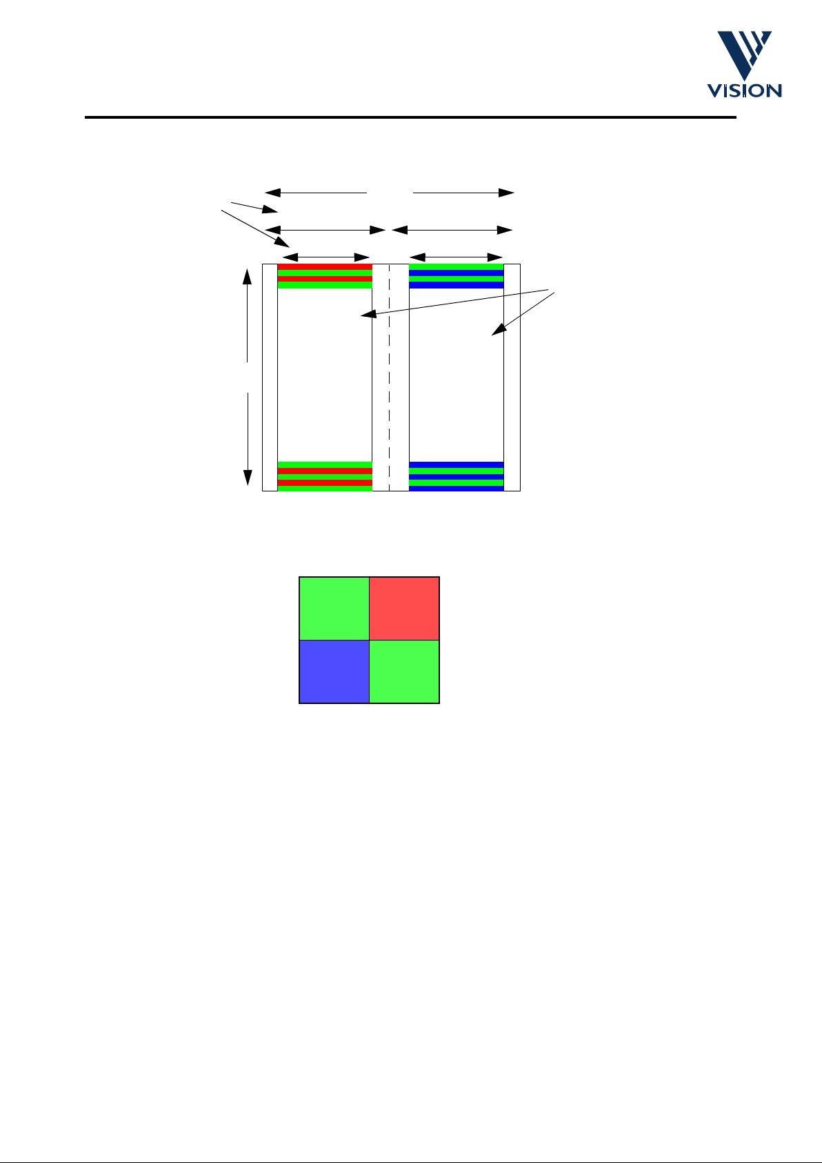
read-out is shuffled to avoid crosstalk between the color channels. The read-out order is all the odd column
pixels followed by all the even column pixels.
note: if this document has not been reproduced on a color printer then the color assignments are as follows:
left region (row numbering from 0 to 127) - red rows 0,2,4,6 etc. green rows 1,3,5,7 etc.
right region (row numbering from 0 to 127) - green rows 0,2,4,6 etc. blue rows 1,3,5,7 etc.
Qualifying the Output Data
Data is output from VV6300 in a continuous stream. By utilising signals, like FST, and key events, like the
start of a line or the end of line, the user can sample and display the image data. QCK is used to sample the
data, as described in the previous section. By default the falling edge of QCK will sample the data, however
it is possible to use both the rising and falling edges of a slow QCK QCK
S
to sample the data.
Different sections of the frame can be enabled by QCK. The options, which are selected via setup register4
in the serial interface, are as follows, firstly the QCK can be disabled, therefore no data will be qualified. This
is the default option.
The second option is to have the QCK free running where all the data is qualified.
128
21..147
168
Qualified Pixels
20..146
.
.
.
.
.
.
.
.
.
bin1 - red
note
bin2 - green
note
bin3 - green
note
bin4 - blue
note
.
.
.
.
.
.
.
.
.
.
1,3,5..167
0,2,4..166
Column number
Shuffled Pixel Readout
Blue Green
Green R ed
Even
Columns
(0, 2, 4,...)
Odd
Columns
(1, 3, 5,...)
Even
Rows
(0, 2, 4,...)
Odd
Rows
(1, 3, 5,...)
Bayer colourisation Pattern.
Page 21
cd34021-a.fm 15/01/98 21
VV6300 Sensor
The third option is to only qualify the image data, which also includes the 2 black calibration monitor lines,
lines 1 and 2 in the frame. This option is further complicated in that extra black lines and the extra border
pixels/lines can be enabled giving the following 4 options:
1. Black lines (1-2) plus image (160 pixels by 120 lines)
2. Black lines (1-8) plus image (160 pixels by 120 lines)
3. Black lines (1-2) plus image (164 pixels by 124 lines)
4. Black lines (1-8) plus image (164 pixels by 124 lines)
The final option is to qualify the embedded frame control sequences as well as the image data. These control
sequences are the 6 bytes at the start and at the end of each image line, where an image line is defined
above. The frame start or status line, image and control sequence pixels, will also be qualified during this
mode.
QCK Exceptions
The output data from VV6300 can be formatted in many ways, as detailed in an earlier section of this
document. Under certain operating conditions the relationship between QCK and the output data is
compromised.
It is vital that the phase relationship between the output data stream and the QCK must be maintained from
line to line, for example ensuring that, if enabled, the line code byte is always qualified by the same edge of
the QCK, clearly only applicable when considering slow QCK qualification. It is known that there are an odd
number of pixel periods in each line of the frame. If the slow QCK is selected then clearly two pixels are
qualified during each QCK cycle resulting in the following modes of operation requiring special care: 4 bit
ADC 8 wire output, 8 bit ADC 8 wire output and 4 bit ADC 4 wire output. During the interline period, when the
data bus is outputting data fixed at FF (8bit ADC) or F (4bit ADC), the phase of the QCK is toggled, this will
occur during every interline period. For the 8bit 8wire or 4bit 4 wire options this change is a simple inversion.
The 4bit 8wire option is not quite as straightforward. During the interline period the QCK signal is changed
from its former state to 1 of 3 other states. In addition 2 out of the 4 possible states are video timing mode
Blue Green
Green Red
Blue Green
Green Red
Blue Green
Green Red
Blue Green
Green Red
1
3
2
0
3
2
1
0
VV6300 Image Format
160 Pixels
120 Pixels
124 Pixels
164 Pixels
0, 1, 2, 3,... ... 160, 161, 162, 163
0, 1, 2, 3,...
... 120, 121, 122, 123
Border Rows and Columns
Pixel Array
Blue Green
Green Red
Blue Green
Green Red
Blue Green
Green Red
Blue Green
Green Red
163162161
160
121
123
122
120
Page 22
cd34021-a.fm 15/01/98 22
VV6300 Sensor
dependent.
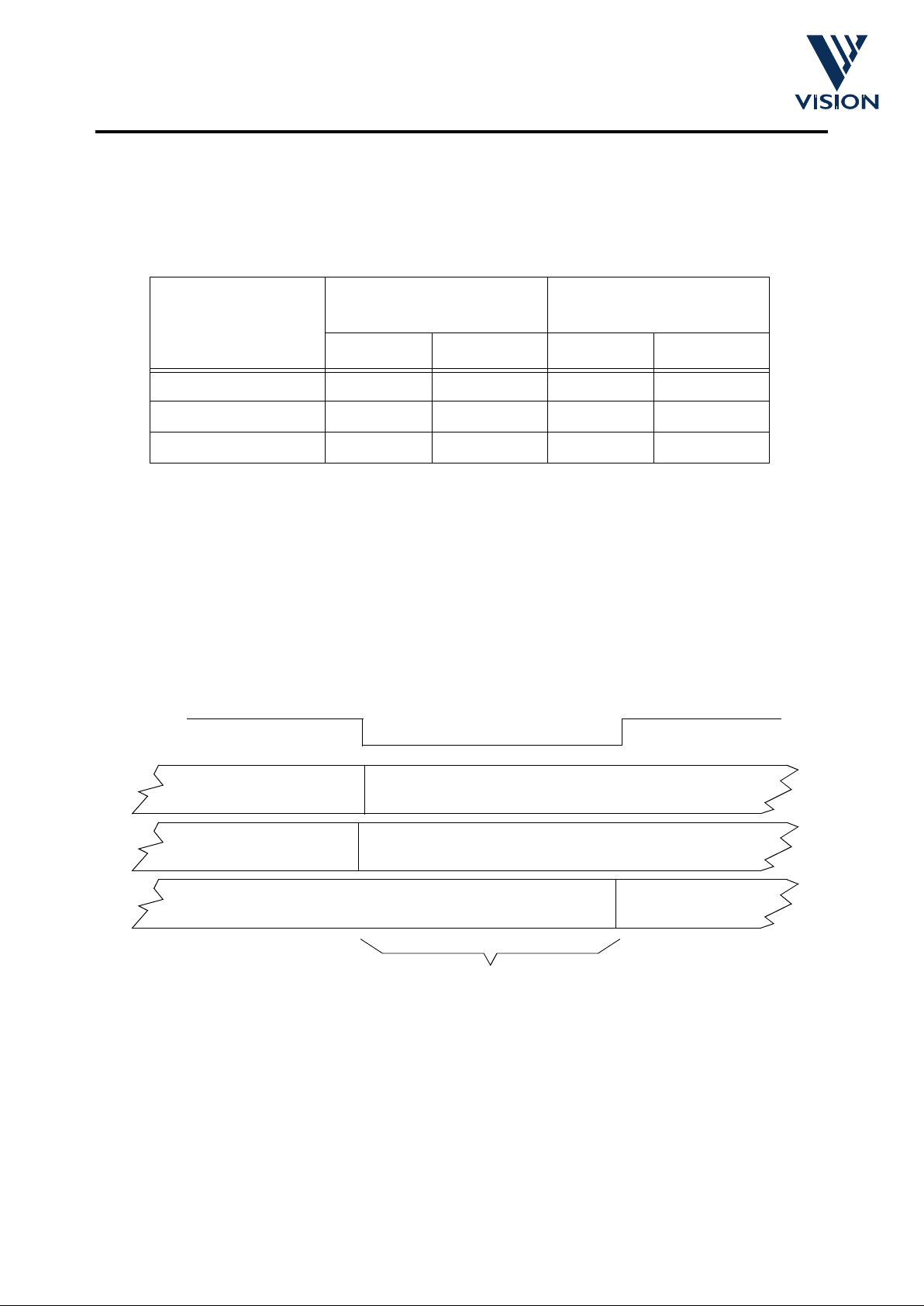
Please note that the number of nibbles/bytes qualified by the clocks described above, during the free running
QCK mode, will differ from the expected value, as follows:
QCK Exception Details
Serial Interface - Exposure Control Handshake
The process of writing timed exposure, clock division or gain settings to VV6300 using the serial interface
requires special attention. These timed parameters can be written to the serial interface at any point within
the frame timing but will only be transferred from shadow registers to their active registers at a specific point
within the frame timing, see diagram below. Please note that writing immediate clock division or gain
parameters are treated as a “normal” serial interface write messages.
Since the new external exposure, clock division or gain settings are written to shadow registers the user
continues to have full read/write access to the serial interface. A handshake system has been implemented
between the exposure controller and the serial interface to avoid the user writing, for example, a second
external timed gain value while the exposure controller has yet to transfer the first external timed gain value
from the shadow register to the active register. If an external timed gain message has been written a special
flag will be raised to indicate that it has yet to be transferred to the active register. This flag is available to the
user via reading the status 0 register in the serial interface. Until the flag is lowered the user knows that it is
not safe to write a further external gain value. Identical handshake protocols are used to implement timed
external exposure and clock division writes.
Operating Mode
Number of pixels qualified
50 frames per second
Number of pixels qualified
60 frames per second
QCK
F
QCK
S
QCK
F
QCK
S
4bit 4wire 203 202 30 1 300
4bit 8wire 202 198 30 0 298
8bit 8wire 203 202 30 1 300
Pixel qualification exceptions
old_exp
old_clock_div
old_gain
odd frame
flag
new_exp
new_clock_div
new_gain
1 frame period
Page 23
cd34021-a.fm 15/01/98 23
VV6300 Sensor
Auto Black Calibration
Black calibration is used to remove voltage offsets that cause shifts in the black level of the video signal.
VV6300 is equipped with an automatic function that continually monitors the output black level and calibrates
if it has moved out of range. Black calibration can be split into two stages, monitor (1 cycle) and update (3
cycles). During the monitor phase the current black level is compared against two threshold values. If the
current value falls outside the threshold window then an update cycle is triggered. The update cycle can also
be triggered by a change in the gain applied to sensor core or via the serial interface.
Serial Interface
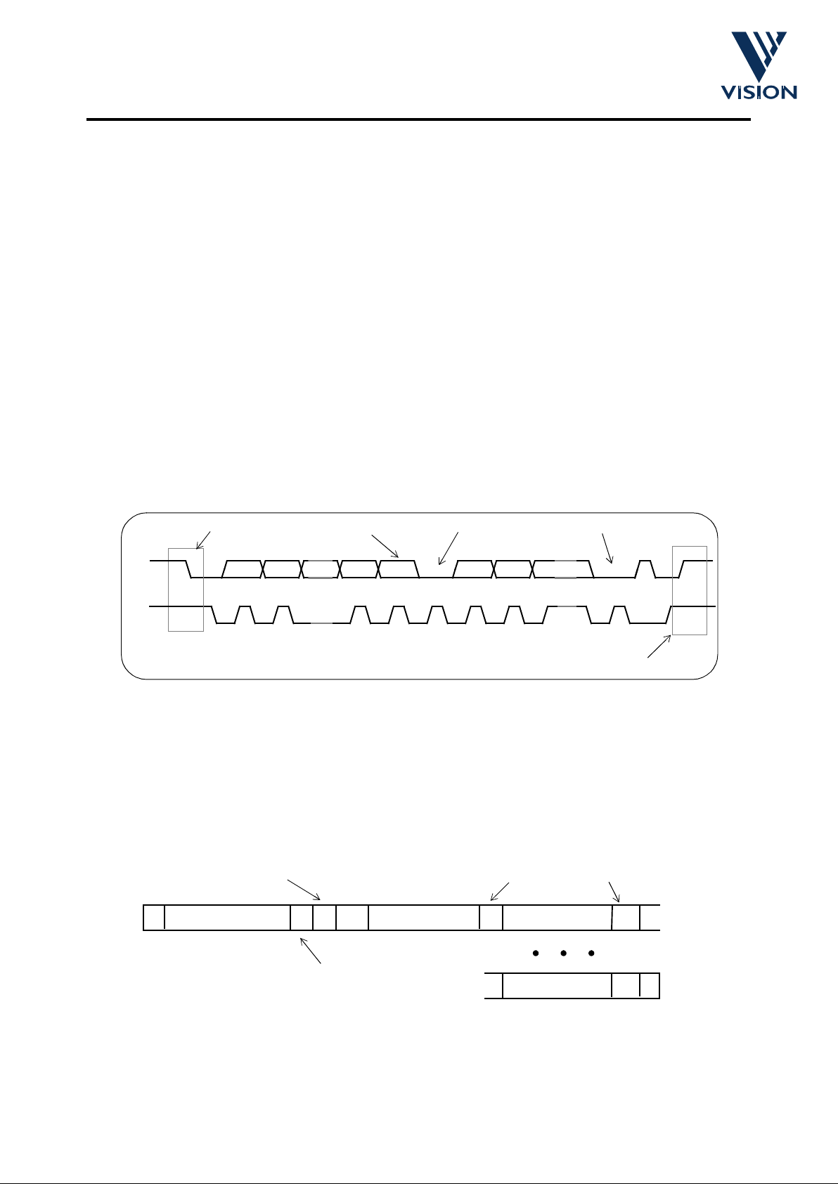
In order to be controlled and configured by its host, VV6300 can receive and transmit data via a two-wire
serial interface.
Serial Communication Protocol
The host must perform the role of a communications master and the camera acts as either a slave receiver
or transmitter.The communication from host to camera takes the form of 8-bit data with a maximum serial
clock frequency of up to 100kHz. Since the serial clock is generated by the host it determines the data
transfer rate. The bus address for VV6300 is 20
H
. Data transfer protocol on the bus is shown below.
Data Transfer Protocol
Data format
A message contains at least two bytes preceded by a
start
condition and followed by either a
stop
or
repeated
start
followed by another message.
The first byte contains the device address byte which includes the data direction read/write bit. The device
address is 32
10
Write, 3310 Read. The 5 msbs of the address byte are fixed as 0010_02. The lsb of the
address byte indicates the direction of the message. An even address causes the addressed slave to receive
information from the master (write), an odd address indicates message read by the master.
Data Format
After the read/write bit is sampled, the data direction cannot be changed, until the read/write bit next message
is received. The next byte contains the location of the first data byte (also referred to as the
index
).There may
be up to 128 such locations. If the msb of the second byte is set the automatic increment feature of the
address index is selected.
1
2
7891
2
3 - 8 9
Start condition
Stop condition
SDA
SCL
MSB
ACK
ACK
Read/Write bit Acknowledge from receiver
P
S
S
address[7:1]
R
/W bit
A
DATA[7:0]
A
Sensor acknowledges valid address
Acknowledge from slave
INDEX[6:0]INC
P
A
A
DATA[7:0]
[0]
0 0 1 0 0 0 0
Page 24

cd34021-a.fm 15/01/98 24
VV6300 Sensor
Message interpretation
All serial interface communications with the sensor must begin with a
start
condition. If the
start
condition is
followed by a valid address byte then further communications can take place. The sensor will acknowledge
the receipt of a valid address by driving SDA low. The state of the read/write bit (lsb of the address byte) is
stored and the next byte of data can be interpreted.
During a write sequence the second byte received is an address index and is used to point to one of the
internal registers. The msbit of the following byte is the
index auto increment
flag. If this flag is set then the
serial interface will automatically increment the index address by one location after each slave acknowledge.
The master can therefore send data bytes continuously to the slave until the slave fails to provide an
acknowledge or the master terminates the write communication with a
stop
condition or sends a
repeated
start
,
(Sr)
. If the auto increment feature is used the master does
not
have to send indexes to accompany the
data bytes.
As data is received by the slave it is written bit by bit to a serial/parallel register. After each data byte has
been received by the slave, an acknowledge is generated, the data is then stored in the internal register
addressed by the current index.
During a read message, the current index is read out in the byte following the device address byte. The next
byte read from the slave device are the contents of the register addressed by the current index. The contents
of this register are then parallel loaded into the serial/parallel register and clocked out of the device by
scl.
At the end of each byte, in both read and write message sequences, an acknowledge is issued by the
receiving device. Although VV6300 is always considered to be a slave device, it acts as a transmitter when
the bus master requests a read from the sensor.
At the end of a sequence of incremental reads or writes, the terminal index value in the register will be one
greater
the last location read from or written to. A subsequent read will use this index to begin retrieving data
from the internal registers.
A message can only be terminated by the bus master, either by issuing a stop condition, a repeated start
condition or by a negative acknowledge after reading a complete byte during a read operation.
The programmers model
There are 128, 8-bit registers within the camera, accessible by the user via the serial interface. They are
grouped according to function with each group occupying a 16-byte page of the location address space.
There are eight such groups, The primary categories are given below:
• Setup registers with bit significant functions incl uding status (read only) bits
• Exposure parameters that influence output image brightness.
• System functions and test bit significant registers.
Any internal register that can be written to can also be read from.
Page 25
cd34021-a.fm 15/01/98 25
VV6300 Sensor
A detailed description of each register follows. The address indexes are shown as binary in brackets.
Index Name R/W Default Comments
Status
000_0000 RO 1100 00002 (C0H)
Reserved
000_0001 RO 0001 0010
2
(12H)
000_0010 status0 RO 0000 1000
2
(08H) System status information
000_0011 unused 000_0100 line_count RO Current line counter value
000_0101 leftav RO Average value of pixels in the first
half of the current line.
000_0110 rghtav RO Average value of pixels in the second
half of the current line.
000_0111 frame_av RO Average value of pixels in a frame.
000_1000 bin1 RO Partial frame average - bin1
000_1001 bin2 RO Partial frame average - bin2
000_1010 bin3 RO Partial frame average - bin3
000_1011 bin4 RO Partial frame average - bin4
000_11xx unused -
Setup
001_0000 setup0 R/W 0010_01112 (27H) Configure the digital logic
001_0001 setup1 R/W 011 1_0000
2
(70H) Configure the digital logic
001_0010 setup2 R/W 0001_1 111
2
(1FH) Pixel counter reset value
001_0011 setup3 R/W 0000_11 11
2
(0FH) Exposure control modes
001_0100 setup4 R/W 0000_0000
2
(00H) FST/QCK options
001_0101 unused -
001_011x unused -
001_1xxx unused -
Exposure
010_0000 unused 010_0001 fine R/W 0000_0000
2
(00H) Fine exposure initially ze ro
010_0010 unused 010_0011 c oa rse R/W 0111_0000
2
(70H) Coarse exposure
010_0100 gain R/W 0000_0000
2
(00H)Gain value
010_0101 clk_div R/W 0000_0000
2
(00H) Clock division
010_0110 gn_lim R/W 0000_0111
2
(07H) Maximum allowable gain
010_0111 tl R/W 0101_0101
2
(55H) Lower exposure control threshold.
010_1000 tc R/W 1001_0110
2
(64H) Centre exposure control threshold.
010_1001 th R/W 0110_0110
2
(73H) Upper exposure control threshold.
010_101x unused -
010_1xxx unused -
System
111_0011 xfav R/W 1000_00002(80H) External frame average
111_0101 dcth R/W 1000_0000
2
(80H) Digital comparator threshold
111_1001 unused
111_1010 unused
111_1011 unused
111_11xx unused
The programmers model
Page 26
cd34021-a.fm 15/01/98 26
VV6300 Sensor
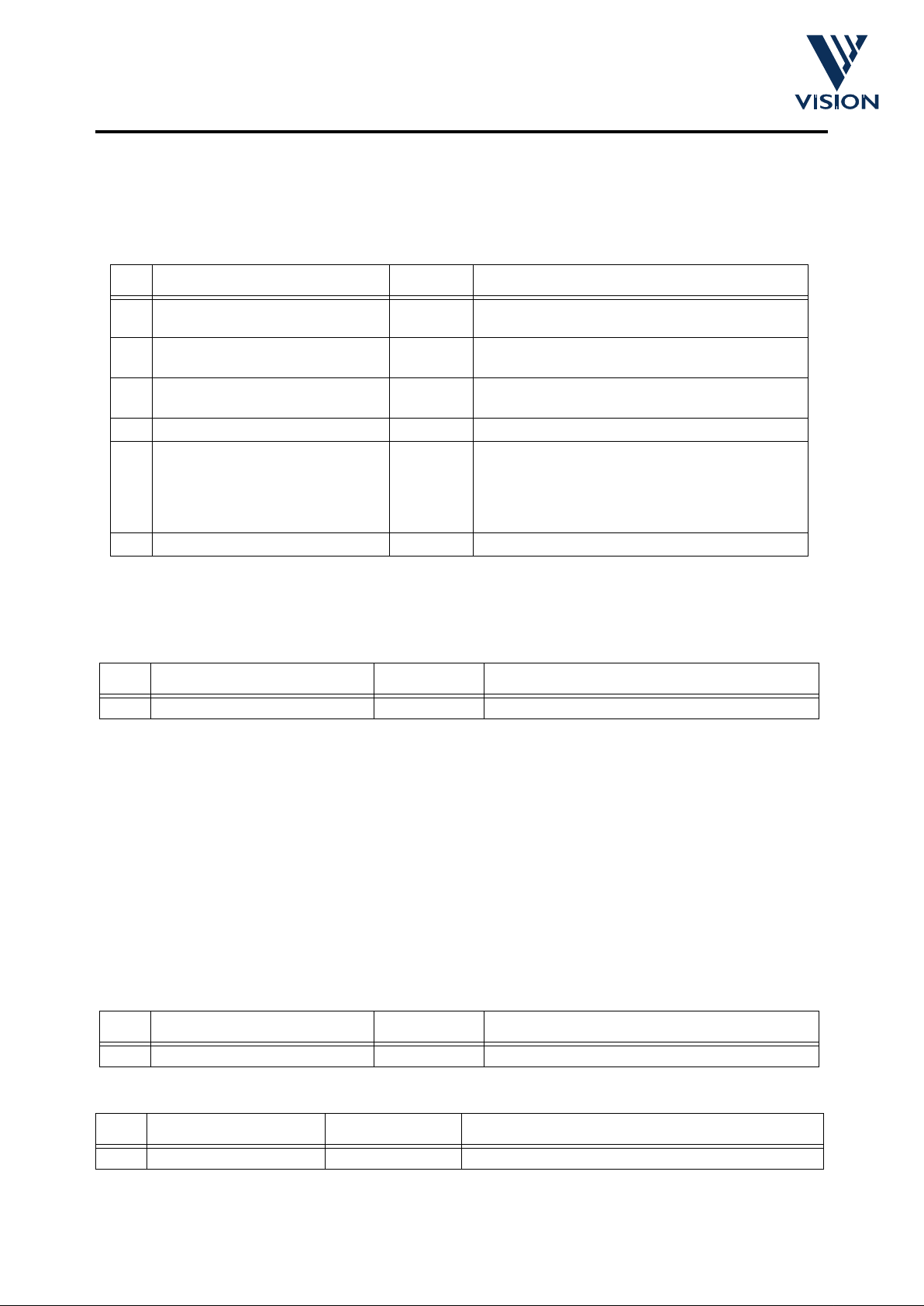
Status 0 [000_00102]
The loading of certain system parameters is timed to avoid disturbing the video signal part way through a
frame. Bits 0-2 can be polled to check that a value written to either the exposure, gain or clock division
registers has been consumed or not. Bit 3 is essentially an internal flag differentiating between consecutive
frames.
Line_count [000_01002]
The video timing logic is controlled by the pixel counter and the line counter. To reduce the level of digital
switching noise these counters implement a gray count sequence, where only a single counter register can
change state in a clock period. However the gray count sequence is user unfriendly,e.q. 248,232,233,
235,234. A binary version of the line count is generated internally, realising a 0,1,2,3,4..... sequence, and it
is this count sequence that is read by the serial interface and hence made available to the sensor user.
Line_avg 0 [000_01012] & Line_avg 1 [000_01102]
The exposure controller accumulates the pixel output values. On a line by line basis the accumulation is
performed in two stages. The qualified pixels in the left half of the video line are accumulated and then stored
in a latch. The process is then repeated during the right half of the video line. During the interline line period
(up until the latch that stores the value for the left half of the line is updated during the next line) the latches
will present valid average 8-bit pixel values for both halves of the line.
Bit Function Default Comment
0 Exposure value update pending 0 New exposure setting sent but not yet con-
sumed by the exposure controller
1 Clock division value update
pending
0 New clock division setting sent but not yet
consumed by the exposure controller
2 Gain value update pending 0 New gain value sent but not yet consumed by
the exposure controller
3 Odd/even frame 0 The flag will toggle state on alternate frames
4 Black Calibration fail flag 0 If the black calibration algorithm returns very
poor black leve ls - o utwi th both the c alibrati on
and monitor windows then this fla g will be set
and it will stay set until the next successful cal-
ibration is complete
7:5 Unused 0
Status 0 [000_00102]
Bits Function Default Comment
7:0 Line count 0000_00002Displays current line count
Line_count [000_01002]
Bits Function Default Comment
7:0 Line average 0 Average pixel value for first half of current line.
Line_avg 0 [000_01012]
Bits Function Default Comment
7:0 Line average 0 Average pixel value for second half of current line.
Line_avg 1 [000_01102]
Page 27
cd34021-a.fm 15/01/98 27
VV6300 Sensor
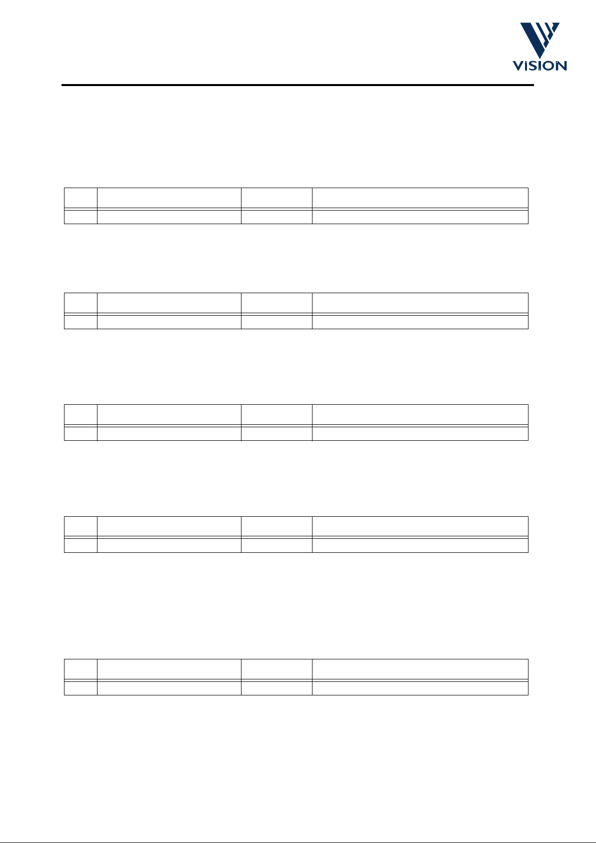
Frame_avg [000 _0 1112]
The average pixel values stored in latches half way through and at the end of each active video l ine
are ultimately stored in bins that will maintain a frame sum of the pixel values. At the end of the
frame the values stored in these bins are used to de termine the overall pixel average for the whole
frame.
Bin1_avg [000_10002]
Bin2_avg [000_10012]
Bin3_avg [000_10102]
Bin4_avg [000_10112]
Bits Function Default Comment
7:0 Frame average 0 Pixel average for previous frame
Frame_avg [000_01112]
Bits Function Default Comment
7:0 Bin1 average 0 Pixel average for current line
Bin1_avg [000_10002]
Bits Function Default Comment
7:0 Bin2 average 0 Pixel average for current line
Bin2_avg [000_10012]
Bits Function Default Comment
7:0 Bin3 average 0 Pixel average for current line
Bin3_avg [000_10102]
Bits Function Default Comment
7:0 Bin4 average 0 Pixel average for current line
Bin4_avg [000_10112]
Page 28
cd34021-a.fm 15/01/98 28
VV6300 Sensor
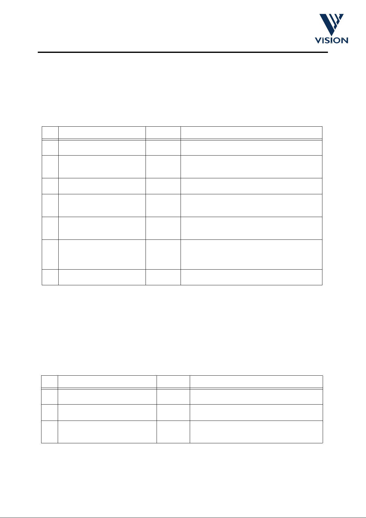
Setup 0 [001_00002]
Setup registers 0,1,2,3 and 4 are used to alter the operating parameters of the sensor. All of these registers
can be written to and read from.
Setup 0 register controls some fundamental exposure and output format parameters. Defaults are shown in
Bold.
Setup 1 [001_00012]
Setup 1 register controls registers that are less likely to be modified on a regular basis. The user should note
that the border pixels/lines can be disabled/enabled independently from the enabling/disabling of the custom
analogue horizontal shift register.
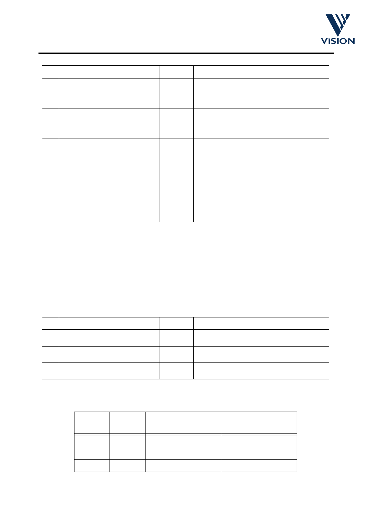
Bit Function Default Comment
0 Automatic exposure control.
Off/On
1 Enables or disable s automatic exposure control.
Current exposure value is frozen when disabled.
1 Clamp fine exposure
Off/On
1 If this bit is set
and
aec is enabled
and
the coarse
exposure has exceede d the clamp th reshold, 16,
then the fine exposure will be clamped to 0.
2 Automatic gain control.
Off/On
1 Enables or disables automatic gain control. Cur-
rent gain value is frozen when disabled.
3 Enable immediate gain
update.
Off/On
0 Allow manual change to gain to be applied imme-
diately.
4 En abl e imm edi ate cl ock div i-
sion update.
Off/On
0 Allow manual change to clock division to be
applied immediately.
6:5 Data format select. 01 00 - 8 wire parallel output
01 - 4 wire parallel output
10 - 2 wire serial output
11 - 1 wire serial output
7 3/4 crystal clock
Off/On
0 Achieves clock division by 3 rather than 4.
Setup0 [001_00002]
Bit Function Default Comment
0 Enable additional black lines (3-8)
Off/On
0 If enabled extra black lines are visible at
device output
1 Enable border pixels
Off/On
0 Extends qualified image size to 164 x 124.
Default image size is 160 x 120
2 E nabl e hor izon t al sh uffle mode.
Off/On
0 The contents of the horizontal shift register
are shuffled so that all th e even c olumns then
all the odd columns are read out.
Setup1 [001_00012]
Page 29
cd34021-a.fm 15/01/98 29
VV6300 Sensor
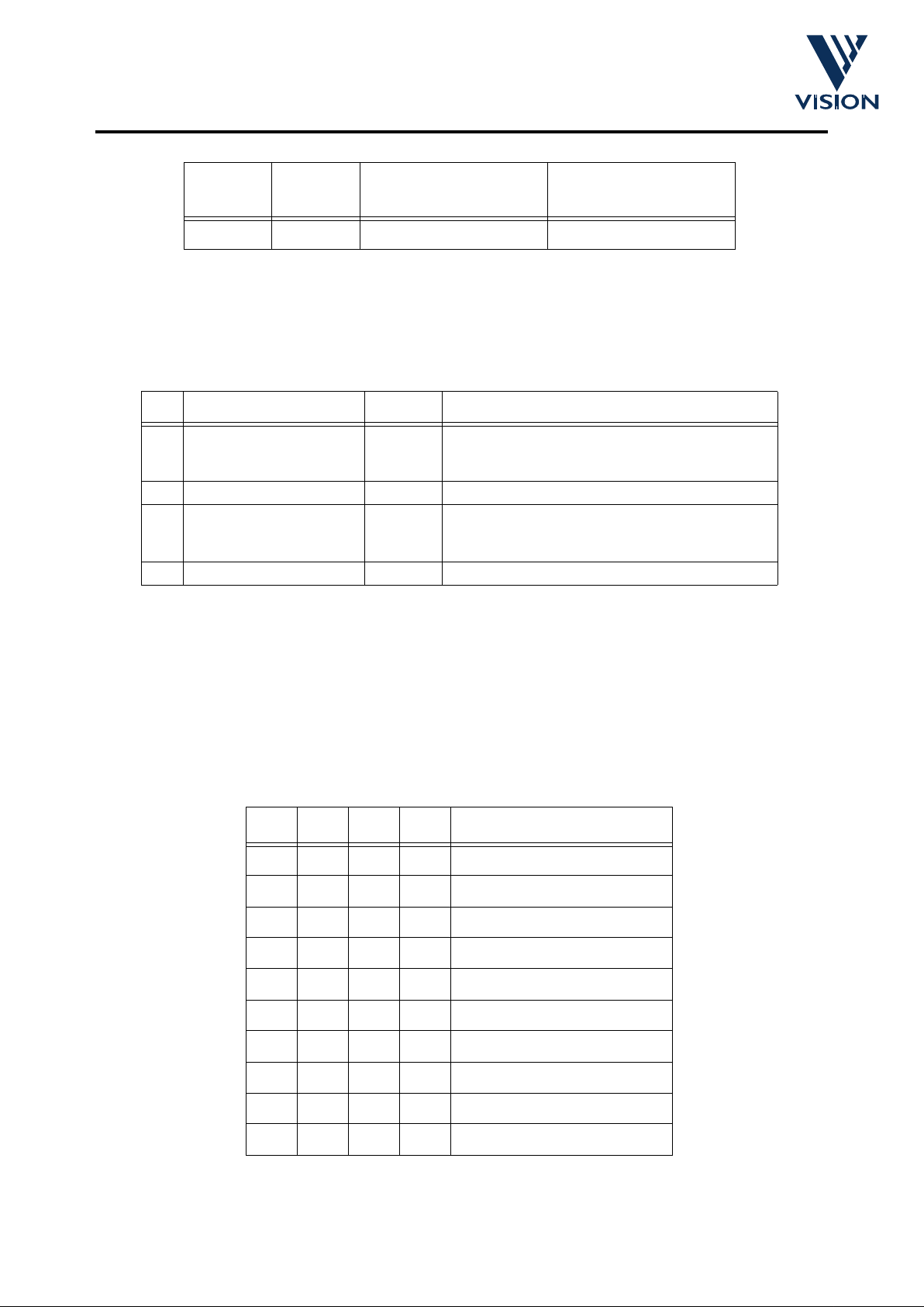
Setup 2 [001_00102]
In many systems VV6300 will be continuously synchronised. During this synchronisation the video timing is
reset to a fixed point within the frame timing. The counter reset value is definable.
3 Enable sample mode
Off/On
0 If enabled the data bus will cont inuously out-
put a “96
H
” pattern. WIth the sensor in this
mode a user can determine the best point at
which to sample the data.
4 Status line data output enable.
Off/On
1 Enables the output of serial interface status
information on the data bus. By default the
bottom 64 locations from the serial interface
will be output.
5 8-bit or 4-bit ADC select 1 The analogue output ADC can be configured
to convert to 4-bit or 8-bit resolution.
6 50fps timing/60fps timing 1 The sensor will implement 60Hz like line
timing by default giving reduced flicker
operation with 60Hz so urce frequencies. If the
supply frequency is 50Hz then 50Hz like
timing should be selected.
7 External frame average
Off/On
0 Normally the accumulator arithmetic logic
calculates the frame average of the pixel
samples. However if this bit is enabled then
the user may specify a frame average.
Bit Function Default Comment
5 :0 P ixel counter reset value. 011111
2
During synchronisation the pixel counter is
reset to the defined value.
6 Status information output option.
Off/On
0 Selects which system parameters are output
on status line. See table below.
7 Status information output option.
Off/On
0 Selects which system parameters are output
on status line. See table below.
Setup 2 [001_00102]
Bit 7 Bit 6
Register Address Range
8-bit modes
Register Address Range
4-bit modes
00 00
H
- 3F
H
00H - 1F
H
01 40
H
- 7F
H
20H - 3F
H
10 - 40
H
- 5F
H
Bit Function Default Comment
Setup1 [001_00012]
Page 30
cd34021-a.fm 15/01/98 30
VV6300 Sensor
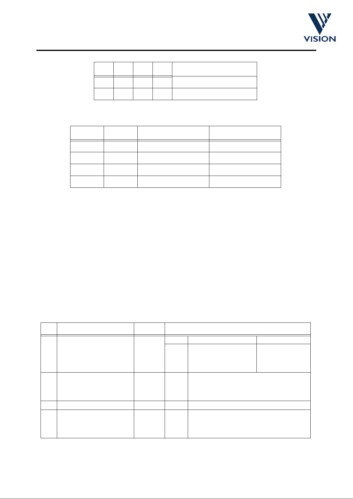
Setup 3 [001_00112]
11 - 60
H
- 7F
H
Bit Function Default Comment
3:0 Exposure control mode
select.
1111
2
The average value for the frame that the
exposure cont roller uses c an be ca lculated in
a number of different ways. See table below.
4 Autoload control 0 This bit controls the autoload feature
.
Note1
6:5 Exposure step size 01 Selects exposure step size. 1/8 for fast but
jerky convergence to 1/64 for slow but smooth
convergence. Default 1/16.
7 Unused 0
Setup 3 [001_00112]
Note1: The state of this pin can affect the autoload function in a number of ways.
1. If the autoload bit is high continuously and the autoload pin is also high then an autol oad will not take place.
2. If the autoload bit is initially high and is then forced low then an autoload will take place regardless of the state of the
autoload p in.
3. If the autoload pin is initially high and is then forced low an autoload will take place regardless of the state of the
autoload b it.
4. A low to high transi tion on ei ther the aut oload bit or th e autol oad pi n while VV6300 i s running w ill have no e ffe ct on th e
autoload function.
Bit 3 Bit 2 Bit 1 Bit 0 Function
0000bin1
0001bin2
0010bin3
0011bin4
0100(bin1 + bin2) / 2
0101(bin3 + bin4) / 2
0110(bin1 + bin3) / 2
0111(bin2 + bin4) / 2
1000(bin1 + bin4) / 2
1001(bin2 + bin3) / 2
Frame Average Options
Bit 7 Bit 6
Register Address Range
8-bit modes
Register Address Range
4-bit modes
Status line information options
Page 31
cd34021-a.fm 15/01/98 31
VV6300 Sensor
Setup 4 [001_01002]
The data output on the serial wire or the 4 wire/8 wire busses can be qualified, if required, by an internally
generated clock signal, QCK. This clock can be configured variously. Both a
fast
and a
slow
QCK can be
generated. If the former is selected then the falling edge of the clock will qualify the current data nibble/byte,
i.e. if the sensor is operating in 4 bit-4 wire mode then any true 8 bit data (e.g. line type code) will be qualified
on a nibble basis. If the
slow
QCK option is preferred then both edges of this clock are used to qualify the
current data nibble/byte.
The QCK function has a dedicated pin assigned, however by selecting the appropriate bits the FST pin can
also output QCK data. By default QCK is disabled. However by writing the appropriate message, QCK can
be forced to free run, qualify the embedded coding sequences and the visible data or the visible data only.
FST can also be enabled or disabled or alternatively the FST pin can output a timing signal to synchronise
several VV6300 sensors or finally the FST pin can output the state of the custom analogue block successive
approximation ADC output comparator.
1010(bin1 + bin2 + bin3 + bin4) / 4
1011(bin1 + bin2 + bin3 + bin4) / 4
Bit 6 Bit 5 Step size Comment
00 1/8
0 1 1/16 Default
1 0 1/32
1 1 1/64
Exposure step size options
Bit Function Default Mode
1:0 FST/QCK pin mode. 00
2
FST pin QCK pin
00
2
01
2
10
2
11
2
Normal FST
Normal FST
QCK
F
Inverted QCK
F
QCK
S
QCK
F
QCK
S
QCK
F
3:2 QCK mode select 00
2
00
2
01
2
10
2
11
2
disable
free running
validate control and image data
validate image data only
5:4 unused 00
2
7:6 FST mode select 00
2
00
2
01
2
10
2
11
2
disable FST
enable FST
synchronisation pulse output (SNO)
output ADC comparator output, CPO
Setup 4 [001_01002]
Bit 3 Bit 2 Bit 1 Bit 0 Function
Frame Average Options
Page 32

cd34021-a.fm 15/01/98 32
VV6300 Sensor
Exposure Control Registers [010_00012] - [010_10012]
There is a set of parameters that control the time that the sensor pixels are exposed. The parameters are as
follows: fine and coarse exposure time, clock division control and finally gain control. The latter parameter
does not affect the integration period rather it amplifies the video signal at the output stage of the sensor core.
An internal automatic algorithm will, if enabled, continually monitor the pixel output and then, if required, use
this data to correct the current exposure.
Manually changing the divisor applied to the incoming crystal clock can alter the effective integration of the
sensor. By slowing the internal clock down the integration period can be increased, i.e. halving the pixel clock
frequency will double the integration period.
If the user wishes to use the automatic exposure algorithm, the automatic exposure control (controlling
fine
and
coarse
exposure) must be enabled. Additional gain control is optional. It is also possible to change the
gain manually via the serial interface even if the exposure is adjusted automatically.
If a user wishes to write an external value to one of the automatic exposure algorithm registers then it is
advised that the automatic control for that register be disabled prior to using the serial interface to write the
external value.
Note:
The external exposure (coarse, fine or gain) values do not take effect immediately. Data from the serial
interface is read by the exposure algorithm at the start of a video frame. If the user reads an exposure value
via the serial interface then the value reported will be the data as yet unconsumed by the exposure algorithm,
because the serial interface logic locally stores all the data written to the sensor.
Between writing the exposure data and the point at which the data is consumed by the exposure algorithm,
bit 0 of the status register is set. The gain value is updated a frame later than the coarse and fine exposure
parameters. The gain is applied directly at the video output stage and does not require the long set up time
of the coarse and fine exposure settings.
The automatic exposure algorithm uses a set of exposure threshold settings. These thresholds may also be
modified by the user to alter the algorithm’s performance. The exposure algorithm uses these thresholds in
a histogram. The three thresholds divide the histogram into 4 regions, very overexposed, overexposed,
underexposed and very underexposed. The pixel data received from the sensor core is compared against
the thresholds to determine the accuracy of the current exposure setting. A series of flags are set to describe
the outcome of the histogram comparison and the new exposure setting can then be derived.
Each exposure parameter is subject to a maximum setting. The fine exposure setting can be clamped to a
fixed value regardless of the decision made by the automatic algorithm. The clamping will occur if the coarse
exposure setting exceeds a predetermined value and the clamping has been enabled via the serial interface.
Bit Function Default Comment
7:0 Fine exposure value 0000_00002 (00H) maximum fine (50Hz mode) = FF
H
maximum fine (60Hz mode) = A8
H
Fine Exposure Value [010_00012]
Bit Function Default Comment
7:0 Coarse exposure value 0111_00002 (70H) maximum coarse (50Hz and 60Hz modes)
91
H
Coarse Exposure Value [010_00112]
Page 33
cd34021-a.fm 15/01/98 33
VV6300 Sensor
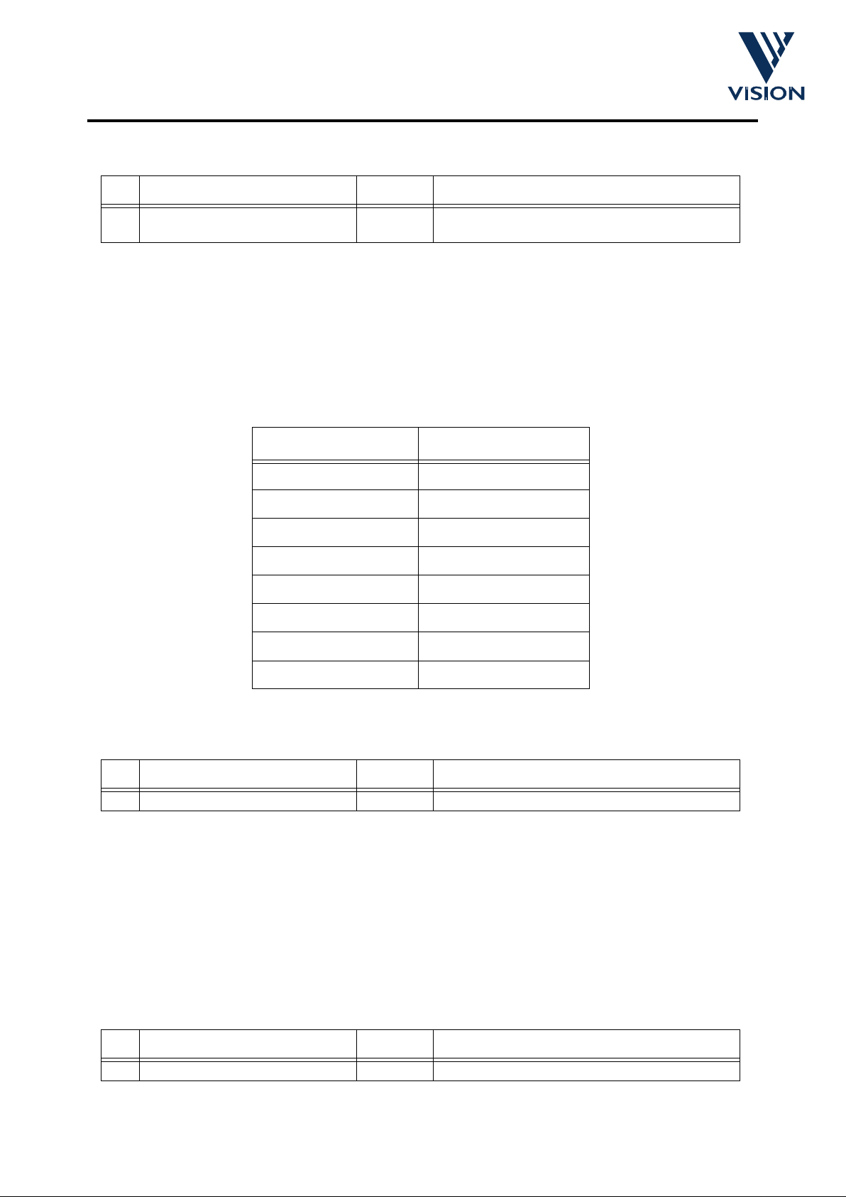
All 8 binary codes can be written to the core via the serial interface. Only the 4 thermometer codes
000,001,011 and 111 are selected by the automatic exposure algorithm. The 4 other codes are however still
valid and will be evaluated as detailed in the table below. It is clear, from the non-linear relationship between
the binary code and the actual gain applied at the analogue output stage, that care should be taken when
using non thermometer code gain settings. If the user writes a gain code of 110 (real gain = 1.600) and then
enables automatic gain control and the controller then decided to reduce the gain, the new gain value would
be 011 (real gain = 4.000) i.e. the effective applied gain at the analogue output stage has actually been
increased.
Bit Function Default Comment
2:0 Gain value 0 8 possible gain states can be written via the
serial interface
Gain Value [010_01002]
Gain binary code Actual signal gain
000 1.000
001 2.000
010 1.333
011 4.000
100 1.143
101 2.667
110 1.600
111 8.000
System Gain
Bit Function Default Comment
1:0 Clock divisor value 0 Pixel clock = Crystal clock ÷2
n+1
Clock Divisor Value [010_01012]
The
undivided
input crystal clock is used by the clock generator circuitry, elements of the serial interface and
a small number of other registers in the design. The remaining digital logic and the analogue circuitry, use
internally generated clocks, namely the pixel clock and the faster ADC clocks. These clocks are all slower
versions of the crystal clock. The ADC clocks may be up to half the crystal frequency, but can be further
divided by factors of 2, 4 or 8. The pixel clock is in turn slower than the ADC clock. If the ADC is operating in
4 bit mode then the pixel clock is 1/4 the frequency of the ADC clock, otherwise the pixel clock will be 1/8 the
frequency of the ADC clock.
Bit Function Default Comment
2:0 Gain limit 7
Gain Limit[010_01102]
Page 34
cd34021-a.fm 15/01/98 34
VV6300 Sensor
Frame Average [111_00112]
The exposure controller normally compiles a frame average from the data received from the core. A complete
frame period is required to produce a frame average. This is clearly unacceptable for simulation and test
purposes. It is possible to manually force a frame average via the serial interface. This feature together with
the ability to curtail the frame duration will allow the behaviour of the exposure controller to be examined in
a realistic simulation period.
This register is read/write compatible
Digital Comparator Threshold [111_01012]
The ADC output from the CAB can be digitally compared against a digital threshold. This threshold is fully
programmable via the serial interface register. If the current ADC output is greater than or equal to the
programmed threshold then the modified ADC output will be forced to the full scale output. The full scale
value is mode dependent:- 224 for 8 bit ADC conversion or 14 for 4 bit conversion. If the current ADC output
is less than the threshold then the modified ADC output will be forced to minimum video. The minimum video
setting (the black level) is again mode dependent:- 16 for 8 bit ADC conversion or 1 for 4 bit conversion.
If this feature is not enabled, (tms[7] = 0), then the ADC output will pass unaltered.
As indicated above the ADC can convert to either 4 bit or 8 bit accuracy. When operating in a 4-bit mode the
threshold value should be packed to the 4 most significant bits of the register i.e. if the required threshold
Bit Function Default Comment
7:0 Exposure lower threshold 85
Exposure Lower Threshold [010_01112]
Bit Function Default Comment
7:0 Exposure centre threshold 100
Exposure Centre Threshold [010_10002]
Bit Function Default Comment
7:0 Exposure higher threshold 115
Exposure Higher Threshold [010_10012]
Bit Function Default Comment
7:0 Frame average 0 Allow a synthetic frame average to be
written to and used by the exposure
controller
Frame Average [111_00112]
Page 35

cd34021-a.fm 15/01/98 35
VV6300 Sensor
value is 10 then 160 should be written to the threshold register.
Bit Function Default Comment
[7:0] Threshold for digital comparator 128 The default has been set at the mid-
range video setting for 8 bit ADC
conversion. The user must reprogram the register if the test is run
when the ADC is converting to 4 bit
accuracy.
Digital Comparator Threshold [111_01012]
Page 36
cd34021-a.fm 15/01/98 36
VV6300 Sensor
Types of messages
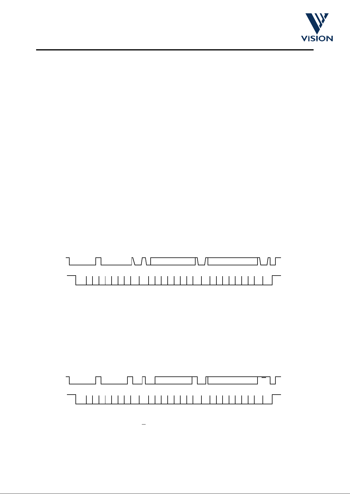
This section gives guidelines on the basic operations to read data from and write data to the serial interface.
The serial interface s upports var iable leng th messages . A message ma y contain n o data byte s, one data b yte
or many data bytes. This data can be written to or read from common or different locations within the sensor.
The range of instructions available are detailed below.
• No data byte, only sets the index for a subsequent read message.
• Single location multiple data write or read for monitoring for real ti me control
• Multiple location, multiple data read or write for fa st information transfers.
Examples of these operations are given below. A full description of the internal registers is given in the
previous section
For all examples the slave address used is 0010000
2
=3210 for writing and 00100012=3310 for reading. This
corresponds to applying logical zero to both the
sab0
and
sab1
inputs.
Single location, single data write.
When a random value is written to the sensor, the message will look like this:
In this example, the
coarse
(index = 01000002=3210) exposure value has been written as 010101012. The r/
w bit is set to zero for writing and the
inc
bit is set to zero to disable automatic increment of the index after
writing the value. The location is preserved and may be used by a subsequent read.
Single location, single data read.
A read message always contains the index used to get the first byte.
This example shows a
coarse
(index = 3210) value of 0101_01012 been read. Note that the read message is
terminated with a negative acknowledge (A
) from the master: it is not guaranteed that the master will be able
to issue a stop condition at any other time during a read message. This is because if the data sent by the
slave is all zeros, the
sda
line cannot rise, which is part of the stop condition.
010_0000
0101_0101
SP
AAA
00100000 0
SP
AA
A
00100001
010_0000 0101_0101
0
Page 37
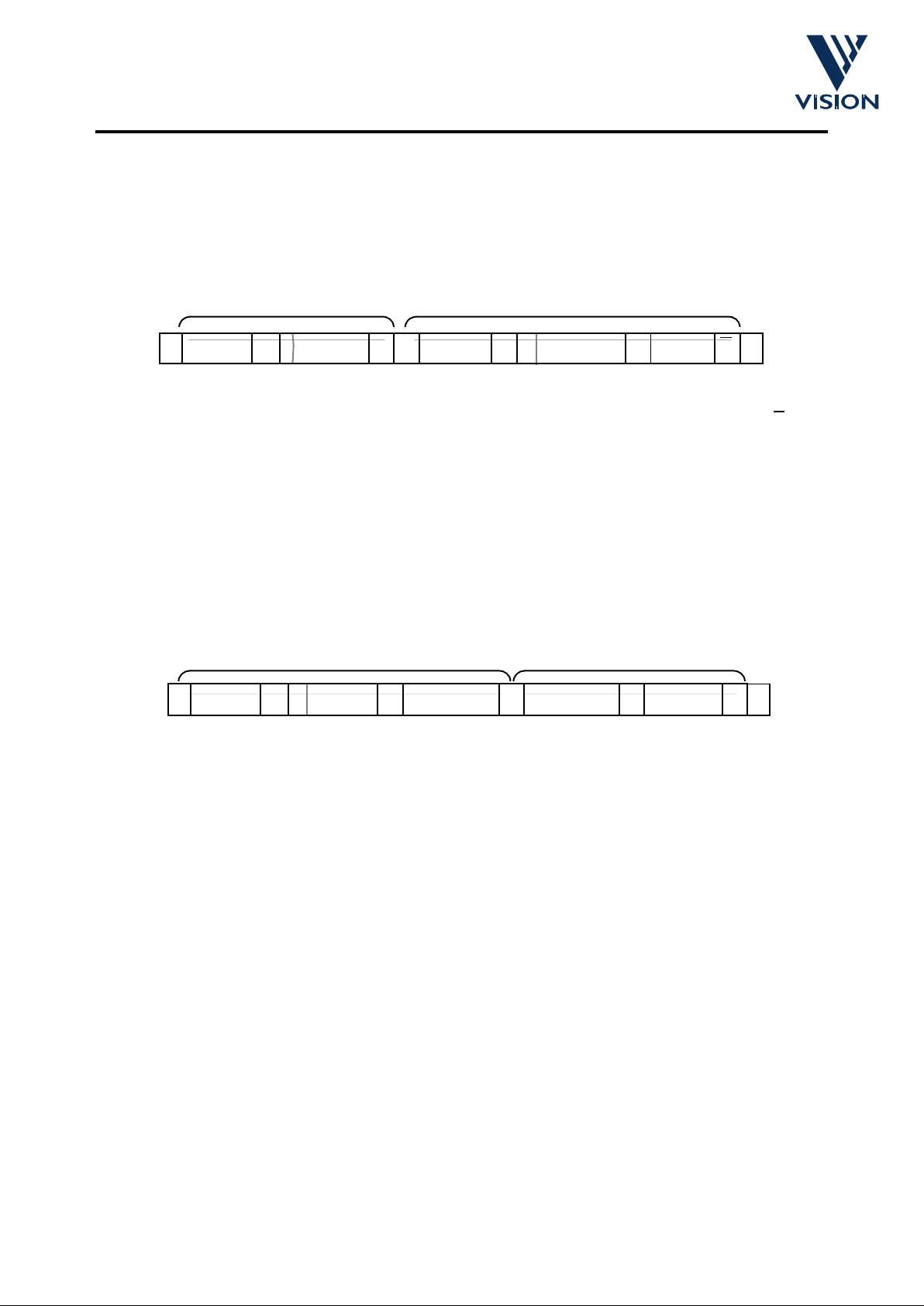
cd34021-a.fm 15/01/98 37
VV6300 Sensor
No data write followed by same location read.
When a location is to be read, but the value of the stored index is not known, a write message with no data
byte must be written first, specifying the index. The read message then completes the message sequence.
To avoid relinquishing the serial to bus to another master a repeated start condition is asserted between the
write and read messages. In this example, the
gain
value (index = 3610) is read as 1510:
As mentioned in the previous example, the read message is terminated with a negative acknowledge (A
) from
the master.
Same location multiple data write.
It may be desirable to write a succession of data to a common location. This is useful when the status of a
bit,(e.g. requesting a new black calibration), must be toggled.
The message sequence indexes
setup1
register and initially turns
ABC
off. The next two data bytes then turn
ABC
on and then finally off again, leaving it in the default state.
Same location multiple data read
When an exposure related value (
coarse, fine, acc
or
gain
) is written, it takes effect on the output at the
beginning of the next video frame, (remember that the application of the
gain
value is a frame later than the
other exposure parameters). To signal the consumption of the written value, a flag is set when any of the
exposure or gain registers are written and is reset at the start of the next frame. This flag appears in
status0
register and may be monitored by the bus master. To speed up reading from this location, the sensor will
repeatedly transmit the current value of the register, as long as the master acknowledges each byte read.
In the next example, a
fine
exposure value of 0 is written, the status register is addressed (no data byte) and
then const antly read until the master terminates the read message.
S
A
Sr A
A
A
P
32
10
36
10
33
10
36
10
1510A
0
0
No data write Read index and data
S
A
0
10
A
A
A20
16
2
10
128
10
0
10
A
0
Write
setup1
Turn off ABC
Toggle “Force Black Cal.”.
P
Page 38
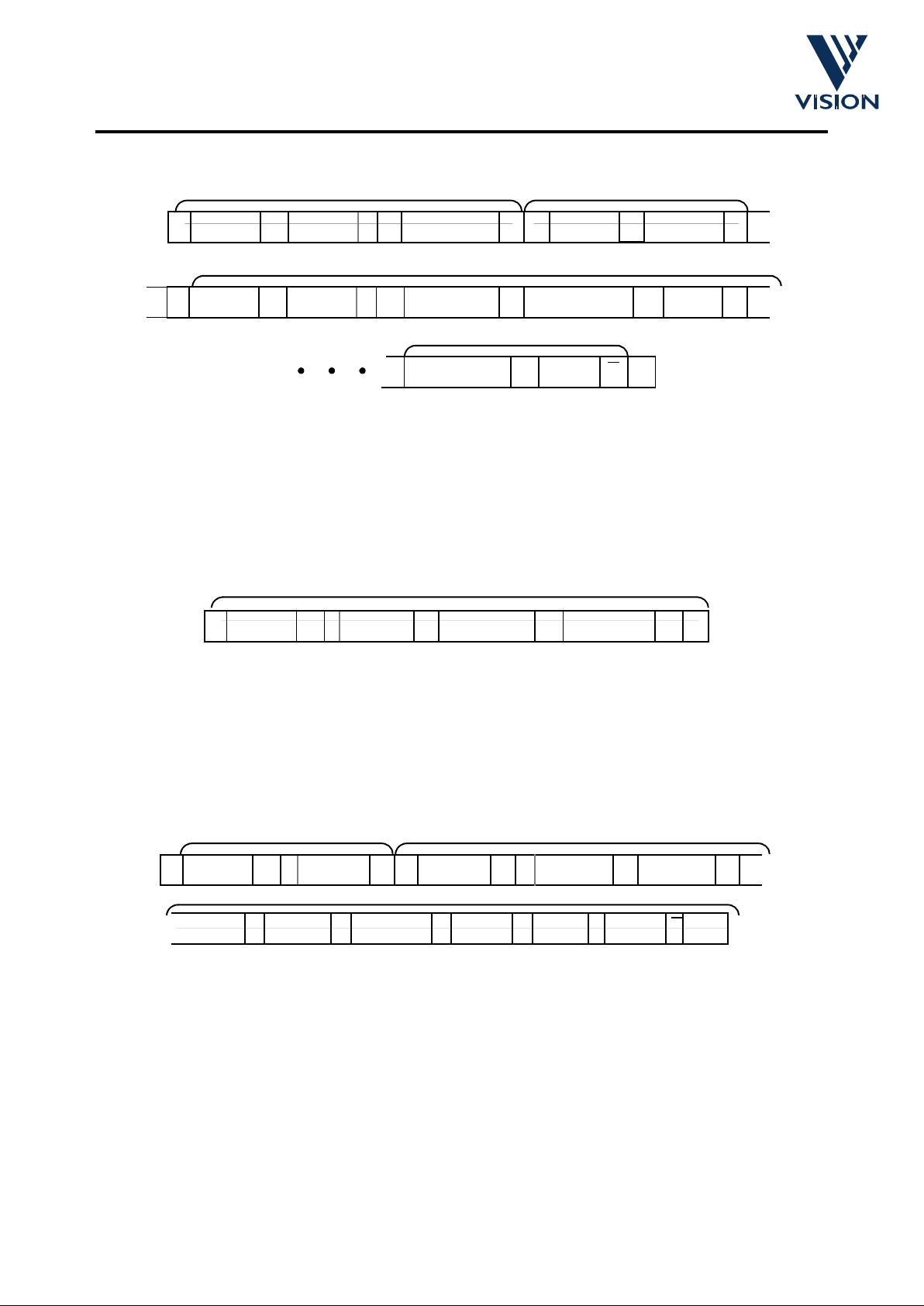
cd34021-a.fm 15/01/98 38
VV6300 Sensor
Multiple location write
If the automatic increment bit is set, msb of the first data byte following the byte that contains the slave device
address, then it is possible to write data bytes to many adjacent internal registers. A write to the black
calibration parameters with their default values is shown in the following example.
.
Multiple location read
In the same manner, multiple locations can be read with a single read message. In this example the index is
written first, to ensure the exposure related registers are addressed and then all seven are read
Note that a stop condition is not required after the negative acknowledge from the master.
S
A
0A
A
A20
16
22
10
20
16
0
10
A
0
Sr
A
A
A
A
21
16
0
10
1
1
1
A
0
Sr
Write
fine
with zero
Address the status0 reg.
A
1
0
A
Read continuously...
...until flag res e t
P
S
A
8
16
A
A
A
20
16
96
10
32
16
1
Incremental write
P
Incremental read
S
A
A
32
10
32
10
1 Sr
33
10
A
A
32
10
1
coarse
A
A
P
fine
gain
gn_lim
T1
Tc
A
AAA
No data write
Incremental read
T2
A
Page 39
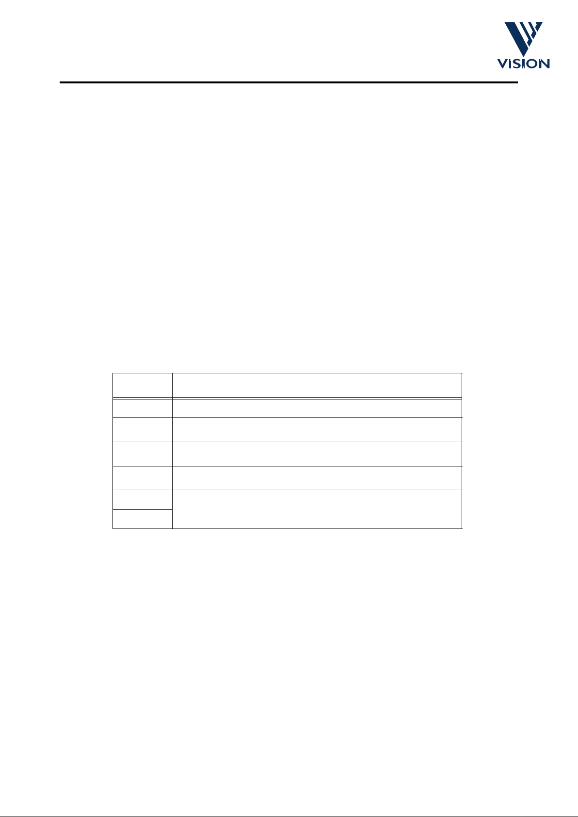
cd34021-a.fm 15/01/98 39
VV6300 Sensor
Serial Inte rface Autoload
VV6300 can be configured automatically at power-up with any user defined set of system parameters using
the serial interface auto-load feature. An external E
2
PROM is used to store the configuration data.
Both shortly after power up and in response to an off-sensor ‘soft’ reset on SIN, the auto-loader will
interrogate the E
2
PROM to determine whether or not valid data is present.
If no E
2
device is detected the auto-loader will shut-down and the serial interface register values will not be
changed from their existing values.
If, however, an E
2
device is detected, the auto-loader will begin to load data into the parameter registers from
starting from location zero in the E
2
.
The first byte is a register header code which determines the destination of the following data byte. This
simple index & data format allows any sub-set of the VV6300 registers map to be configured at power-up and
it allows them to be stored in the E
2
in any order.
If the auto-loader detects the ‘end-of-PROM-contents’ code 00h followed by FFh, it will then issue a STOP
condition on the serial interface, raise a flag to indicate that the parameters have been loaded and close
down.
Header ROM contents
XXh Register
DDh
Data
XXh
Register
DDh
Data
00h
Termination
FFh
Example E2PROM Contents
Page 40
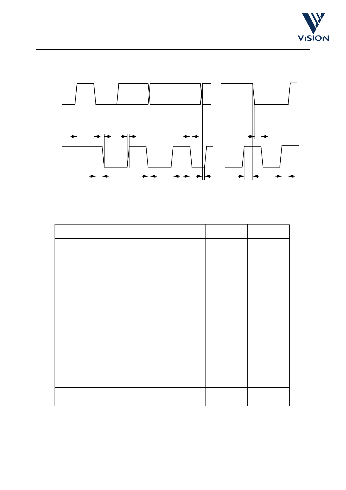
cd34021-a.fm 15/01/98 40
VV6300 Sensor
Serial Inte rface Timing
Serial Interface Timi ng C harac t eris ti cs
Serial Interface Timing Characteristics
Parameter Symbol Min. Max. Unit
SCL clock frequency fscl 0 *** kHz
Bus free time between a
stop and a start
tbuf *** - us
Hold time for a repeated
start
thd;sta *** - us
LOW period of SCL tlow *** - us
HIGH period of SCL thigh *** - us
Set-up time for a repeated
start
tsu;sta *** - us
Data hold time thd;dat *** - us
Data Set-up time tsu;dat *** - ns
Rise time of SCL, SDA tr - *** ns
Fall time of SCL, SDA tf - *** ns
Set-up time for a stop tsu;sto *** - us
Capacitive load of each
bus line (SCL, SDA)
Cb - *** pF
SDA
SCL
thd;sta
tr
thightftsu;datthd;dat tsu;sta tsu;sto
...
...
thd;statlowtbuf
stopstartstop start
all values r eferred to the minimum input level (high) = 3.5V, and maximum input level (low) = 1.5V
Page 41

cd34021-a.fm 15/01/98 41
VV6300 Sensor
This Page intentionally left blank.
Page 42
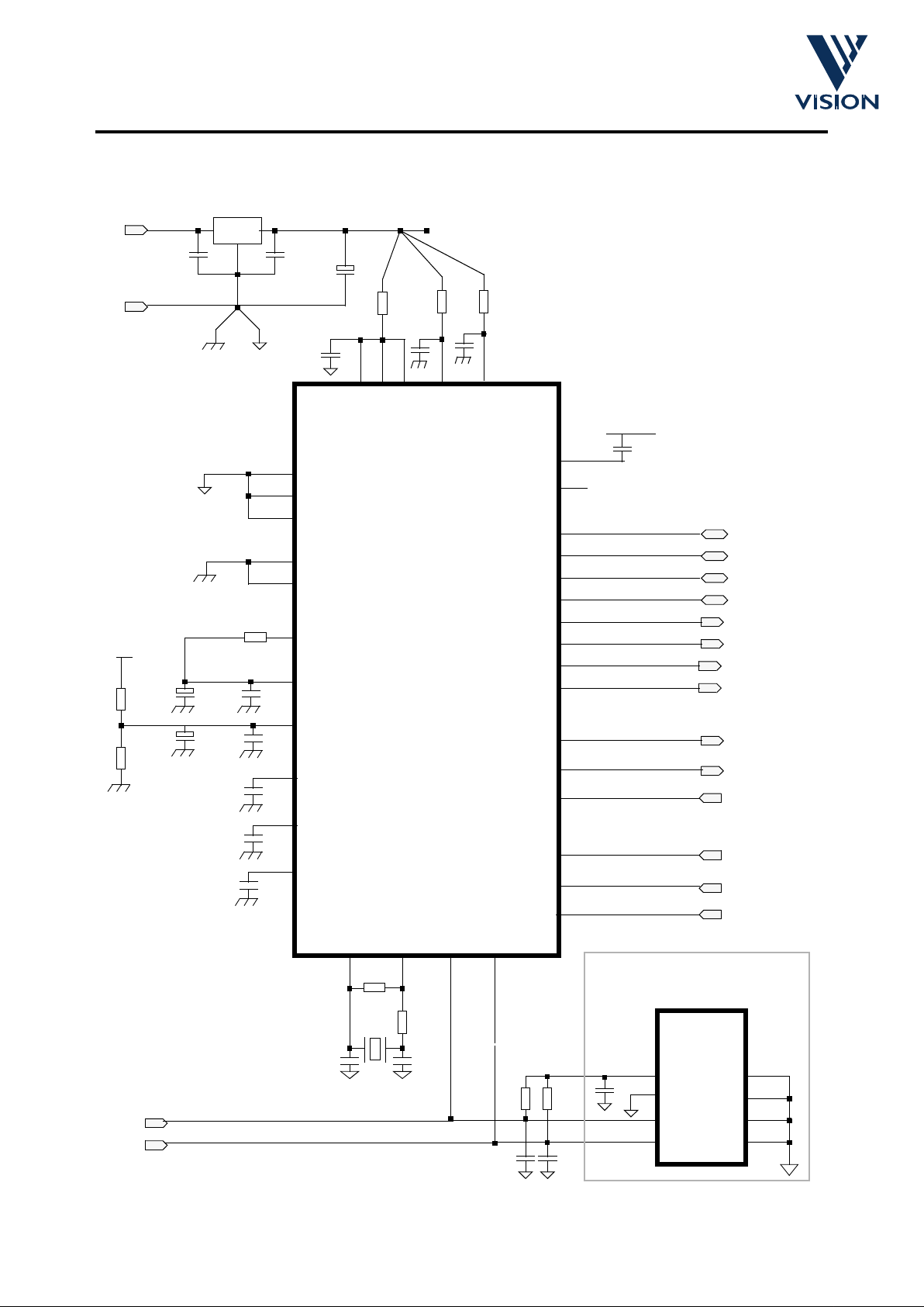
cd34021-a.fm 15/01/98 42
VV6300 Sensor
EXAMPLE SUPPORT CIRCUIT
0v
C1 C2
C3
C4
IC1
3231
2
47
9
28
46
45
15
19
(48 pin LCC)
22
21
3334
20
29
36
27
R1
1
C5
24
23
25
26
SDA
SCL
SDA
SCL
D[7]
VRT
VCDS
HPIX
VBLTW
DVDD
VCM/VREF2V5
VBG
QCK
FST
SIN
VSS1
VSS2
VDD2
VDD1
4
17
16
CLKI
CLKO
C11
C8
C12
AVCC
30
C7
Vin
GND
+8 to +12v dc
C9
R2
VV6300
R4
D[6]
D[5]
D[4]
D[3]
D[2]
D[1]
D[0]
AUTOLOADB
38
CE
37
SIN
CE
FST
QCK
D[0]
D[1]
D[2]
D[3]
D[4]
D[5]
D[6]
D[7]
HPIX
TEST
3
TEST
DVSS
A0VCC
TEST
SCL
A1
A2
SDA GND
E2PROM
6
5
8
7
3
4
1
2
IC3
C16
R5
R6
Optional E2 for configuration
autoload
AGND
VSS3
6
35
VDD3
14
13
C6
R3
R7
R8
C17
C16
44
VBLOOM
C10
40
VREG
C17
IC2
C13
VDD
C18
C14
C15
5V
R9
R10
5V
Page 43
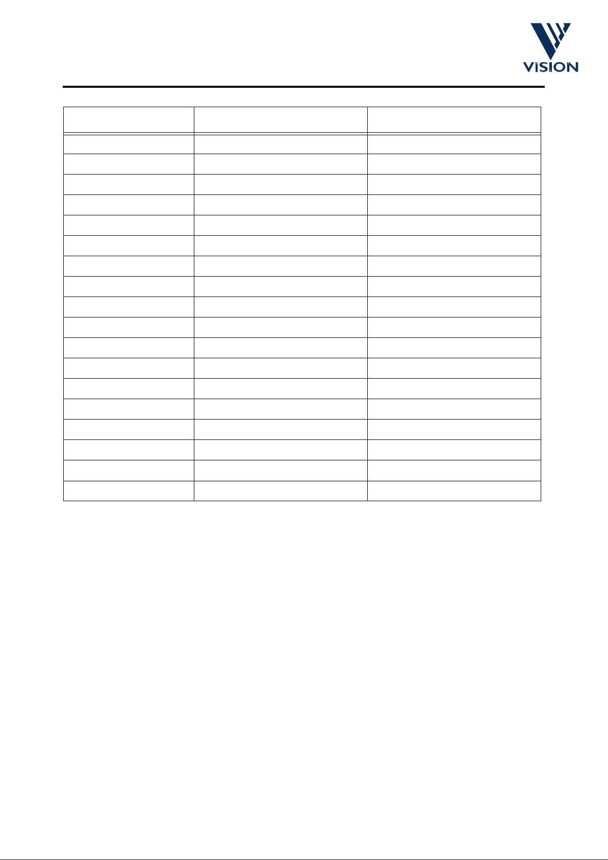
cd34021-a.fm 15/01/98 43
VV6300 Sensor
Component Part No. / Provisional Value Rating / Notes
IC1 VV6300 Vision camera chip (48 pin LCC)
IC2 7805 5V regulator
IC3 24C01 E2PROM SOIC (8 pin)
C3 10.0 µF
C1,C2, C4-C11 0.1 µF
C12, C13 4.7 µF
C14, C15 100pF
C16, C17 22pF
C18 1nF
R1 0Ω
R2 0Ω
R3 0Ω
R4 33Ω
R5, R6 2k2Ω
R7 1MΩ
R8 10Ω
R9 1k8
R10 4k7
Page 44

cd34021-a.fm 15/01/98 44
VV6300 Sensor
VLSI VISION LIMITED
VLSI Vision Ltd. reserves the right to make changes to its products and specifications at any time. Infor mation fur nished by VI SION is bel ieved to be ac curate, but no responsibility is assumed by VISION for the use of said information, nor any infringements of patents or of any other third party rights which
may result from said use. No license is granted by implication or otherwise
under any patent or patent ri ghts of any VISION group company.
© Copyright 1996, VLSI VISION
VLSI Vision agent or distributor
UK Headquarters
Aviation House,
31 Pinkhill,
EDINBURGH
EH12 7BF
Scotland
Tel:+44 (0) 131 539 7111
Fax:+44 (0)131 539 7141
eMail: [email protected]
USA Western Office
1190 Saratoga Ave.,
Suite 180,
SAN JOSE
CA 95129 USA
Tel: +1 408 556 1550
Fax: +1 408 556 1564
eMail: [email protected]
USA Eastern Office
571 West Lake Avenue,
Suite 12,
BAY HEAD
NJ 08742 USA
Tel: +1 732 701 1101
Fax: +1 732 701 1102
eMail: [email protected]
 Loading...