

Page 1
cd24082b.fm 09/09/98: PRELIMINARY 1
Preliminary
The VV5801 (monochrome) and VV6801 (colour) products
offer both high resolution and enhanced performance
levels.
The VV6801 colour sensor has been developed principally
to address the demands of the high resolution colour
Digital Stills camera market. It provides high colour fidelity
with low colour aliasing which is particularly relevant for
stills photography.
The VV5801 monochrome device is ideal for Machine
Vision applications. The functionality of the sensor is
identical to the VV6801, with higher sensitivity.
Control and readout timing requirements are similar and
pinout is backwardly compatable to the VV6850/5850
800K pixel sensors, giving ease of design into existing
VV6850/5850 800K pixel applications. The VV6801 and
VV5801 have an identical image array size to the VV6850/
5850, allowing for existing optics to be used.
All clocking and sequencing controls are used defined,
giving maximum flexibility of use. This gives a range of
versatile operating modes which can be implemented,
including high quality still image capture, full resolution
‘Live Video’, and exposure monitoring modes. A choice of
Horizontal and Vertical subsampled ‘Cine’ modes are
available for increased framerate, ideal for viewfinder
applications.
Both the colour and monochrome devices are suited to
digital still capture and applications requiring digitisation of
the pixel output and post processing of the image in
hardware or software. The image quality from both
sensors can be enhanced by implementation of external
noise cancellation techniques, using external frame and
line buffering.
Exposure control can be achieved with or without an
electromechanical shutter. Both sensors benefit from a
pixel fill factor of more than 25%, which have resulted in
improved sensitivity. A two way serial interface and control
register provides further control and monitoring of certain
camera functions.
• High resolution (1300K) CMOS sensor
designed for use in Digital Colour Stills Cameras and Machine Vision applications
• Versatile operating modes, including ‘Live
Video’ mode, Horizontal Cine mode, and new
Vertical
Cine modes for viewfinder applica-
tions, as well as exposure monitoring modes
• Digital control of pixel reading for flexibility,
including external ADC interface
• Control/configuration via serial interface
• External frame/line buffering schemes offer
effective pixel offset cancellation and low
noise operation
• Bayer pattern R,G,B colourisation (other patterns/colours can be accommodated)
• Monochrome version available - VV5801 functionally identical to the VV6801, but with
higher sensitivity
• Low power operation (125mW Typical)
• Industry standard 84 pin LCC and BGA packages
Image Format 1024 x 1280 pixels
Pixel Size 8.4 x 8.4µm
Active array Size 8.60 x 10.75mm
Sensitivity (colour) 50mV/lux @ 50ms exp.
S/N Typically 66dB (with FPN can-
cellation)
Max. pixel rate 10Mpix/s (5Mpix/s for 0.1% set-
tling)
Power Supply 5v ±5%
Power < 150 mW
Temperature 0
o
C - 40oC
Package BGA or 84LCC
TECHNICAL SPECIFICATION
GENERAL DESCRIPTION
High resolution CMOS 1300K Pixel Image Sensor with support
for external FPN
cancellation and serial interface control, avail-
able in colour (VV6801) and monochrome (VV5801) versions.
VISION
VV6801 & VV5801 Sensors
PRELIMINARY CUSTOMER DATASHEET Revision 1.1
CHARACTERISTICS
cd24082b.fm 09/09/98: PRELIMINARY 2
VISION VV6801/5801 PRELIMINARY CUSTOMER DATASHEET Rev 1.1
Pr
e
l
i
mi
na
ry
Table of Contents
1. General description........................ .. ... .. .... . .... . .... .. ... .. ... .. ... .. .... . .... .. ... .. ... .. ... .. .... . .... .. ... .. ................4
1.1 Sensor architecture........................................................................................................................4
1.2 Typical application....................... ... .. ... .. .... . .... . .... .. ... .. ... .. ... .. .... . .... .. ... .. ... .. ... .. .... . .... .. ... ..................4
1.3 Pixel array......................................................................................................................................5
1.4 Video Output..................................................................................................................................5
1.5 Serial Interface...............................................................................................................................5
2. Architectural details.......................................................................................................................6
2.1 Sensor array...................................................................................................................................6
2.2 Reset and Read Vertical Shift Registers...................... . .... ... .. ... .... .. ... .... . .... ... .. ... .... .. ... .... . .... ... .. ....7
2.3 Horizontal Shift Register.................................................................................................................8
2.4 Pixel Readout Architecture.............................................................................................................9
2.5 Video Output..................................................................................................................................9
2.6 The Video Output Chain...................... .. .... . .... . .... .. ... .. ... .. ... .. .... . .... .. ... .. ... .. ... .. .... . .... .. ... .. ... .. .........10
2.7 AVO Reference............................................................................................................................10
2.8 The 5-Bit DAC..............................................................................................................................11
2.9 Black Reference Lines.................................................................................................................12
3. Exposure Control..........................................................................................................................14
4. Removing Noise............................................................................................................................15
4.1 Sources of Fixed Pattern Noise....................................................................................................15
4.2 Methods of Removing Fixed Pattern Noise..................... ... .... .. ... .... . .... ... .. ... .... .. ... .... . .... ... .. ... .... ..15
5. Operating Modes..........................................................................................................................17
5.1 Still Image Capture with a Frame Buffer......................................................................................17
5.2 Correlated Double Sampling (line by line)....................................................................................18
5.3 Live-Video Mode......................... ... .. ... .. .... . .... . .... .. ... .. ... .. ... .. .... . .... .. ... .. ... .. ... .. .... . .... .. ... .. ..............19
5.4 Cine Modes..................................................................................................................................20
5.5 Parallel Integration.......................................................................................................................21
5.6 Accumulate...................................................................................................................................22
5.7 Multiple Dark Current Periods......................................................................................................22
6. The Control Register & Serial Communication..........................................................................24
6.1 General description......................................................................................................................24
6.2 Serial Communication Protocol....................................................................................................24
6.3 The Serial Data Word...................................................................................................................25
6.4 Register description......................................................................................................................25
6.5 Control Register Definitions..........................................................................................................26
7. Detailed Operational Timing........................................................................................................28
7.1 System Clocks..............................................................................................................................28
7.2 Line Start to PCK Timing..............................................................................................................28
7.3 Initial Power Up Timing................................................................................................................28
7.4 Inter-Frame Timing.......................................................................................................................29
7.5 Line Read-Out Timing............................... ... ... .. .... ... .. ... .... . .... ... .. .... ... .. ... .... . .... ... .. .... ... .. ... ...........30
7.6 Line Timing using CDSR..............................................................................................................34
8. Detailed Specifications................................................................................................................37
8.1 Absolute Maximum Ratings..........................................................................................................37
8.2 DC Operating Conditions.............................................................................................................37
8.3 AC Operating Conditions..............................................................................................................37
8.4 Electrical Characteristics..............................................................................................................38
8.5 Video Output Characteristics........................................................................................................38
Page 2
cd24082b.fm 09/09/98: PRELIMINARY 3
VISION VV6801/5801 PRELIMINARY CUSTOMER DATASHEET Rev 1.1
Pr
e
l
i
mi
na
ry
9. Pin descriptions and Package Details..................................................................................... .. .39
9.1 Pin List........................ .................................................... .............. .............. .......................... ........40
9.2 Package dimensions ....................................................................................................................42
10. Support circuits and design guidelines......................................................................................43
10.1 ADC Interface Circuit....................................................................................................................43
10.2 Analogue Reference Buffering ..................................................................................................... 44
11. Evaluation kit (EVK)........ ............... .......................... .............. .............. .............. .......................... .45
11.1 Key features.................................................................................................................................45
11.2 Block Diagram..............................................................................................................................45
12. Ordering details............ .................................................... .............. ............... .............. . ............. ...46
cd24082b.fm 09/09/98: PRELIMINARY 4
VISION VV6801/5801 PRELIMINARY CUSTOMER DATASHEET Rev 1.1
Pr
e
l
i
mi
na
ry
1. General description
The VV6801 sensor has been developed specifically for use in image processing applications requiring pixel
by pixel access. Flexible control options allow many operating modes, but the VV6801 is ideally suited to
Digital Stills Cameras with a frame store memory available for pixel offset noise cancellation, and ideally an
electromechanical shutter for exposure control and dark current / reset noise cancellation (see Section 4.)
The VV5801 monochrome sensor is identical in operation to the VV6801, but with higher sensitivity and
simpler image processing, due to the absence of colour filters. It is ideally suited to machine imaging
applications.
1.1 Sensor architecture
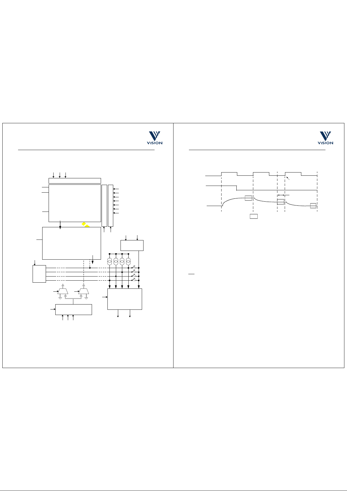
Figure 1.1 : Block diagram of VV6801/5801
1.2 Typical application
Figure 1.2 : Typical digital stills application
SAMPLE & HOLD
HORIZONTAL SHIFT REGISTER
VIDEO OUTPUT STAGE
PHOTODIODE ARRAY
REF. VOLTAG ES
CONTROL CCTS.
VRT
Vbltw
Vbloom
VRTRef
Vbloomref
COLSam
Vbltwref
VBG
AVO
VERTICAL SHIFT REGISTERS
FR
DOUT
SERIAL
I/F
DLAT
DCK
DIN
PXRD
CDSR
EVWT
RESETB
5-Bit DAC
CONTROL REGISTER
AVORef
LCK
EVEN
FI
VCLRB
VSETB
PCK LS EC HCLRB
Cine Modes
SELRef
SAMRef
CLAMP
VCL1
VCL2
(UNBUFFERED)
1306 X 1028
(1280 x 1024 valid pixels)
Timing
DSP
I/O Processing
Frame Buffer
Picture
Storage
Lens
Sensor
ADC
Exposure Control
Shutter
Flash
ASIC/DSP
(Image/colour
processing)
Timing & Control
Serial Data
Page 3
cd24082b.fm 09/09/98: PRELIMINARY 5
VISION VV6801/5801 PRELIMINARY CUSTOMER DATASHEET Rev 1.1
Pr
e
l
i
mi
na
ry
1.3 Pixel array
The pixel array is colourised in a four pixel, Red, Green, Blue ‘Bayer’ arrangement. This provides high colour
fidelity images with low colour aliasing. The pixel array includes a number of reference lines, and a useable
image area of 1280 x 1024 ‘valid video’ pixels.
Pixel access is by row and column shift registers. Each row of pixels, or line, is read at the same instant, and
stored in a sample-and-hold stage. The columns are then read out alternately, and multiplexed through four
output channels to the AVO output stage. The image can then be unshuffled and reconstructed in external
buffering and processing circuits.
This scheme provides AVO settling to better than 0.1% at a sampling rate of 5 Msps. (Higher sampling rates
are possible, with reduced settling accuracy.
1.4 Video Output
The multiplexed column outputs are buffered to the Analogue Video Output (AVO) pin, as ‘inverted’ video,
that is Black is higher than White. An AVORef output is also generated, from the internal black reference
level, to provide a pseudo differential output pair.
A DC component is added to the AVO and AVORef signals at the AC coupled output stages by CLAMPing
these to VCL1 and VCL2, one of which can be set by an internal DAC. This allows the AVO level to be
matched to the input range of an external ADC.
1.5 Serial Interface
The serial interface allows an external controller to set certain parameters and to determine the VV6801’s
current state. This is done through the Control Register, which is loaded from DIN and examined at DOUT.
The VV6801 receives serial data as one 22-bit data word, the 20 msb of which are clocked into a shift register.
The shift register contents can then be latched into the Control Register.
cd24082b.fm 09/09/98: PRELIMINARY 6
VISION VV6801/5801 PRELIMINARY CUSTOMER DATASHEET Rev 1.1
Pr
e
l
i
mi
na
ry
2. Architectural details
2.1 Sensor array
The VV6801 image sensor comprises an array of 1306 (vertical, ‘lines’) by 1028 (horizontal) active
photodiode cells feeding into a row of column source followers at the top of the pixel array. These columns
are then in turn multiplexed on to four output channels, and finally onto the AVO output. Exposure, that is
pixel integration time, is controlled by a ‘Reset Vertical’ shift register with pixel readout controlled by the ‘Read
Vertical’ and ‘Horizontal’ shift registers.
The first (‘bottom’) 6 lines of the array are black reference lines, followed by 8 colour characterisation lines,
2 ‘dummy’ lines, 1280 valid video lines, 2 further ‘dummy’ lines, then 8 further colour characterisation lines at
the ‘top’ of the array. The outer two columns on the left and right sides of the pixel array are also internal
references, and not read out. Thus the usable image area of the 1306 x 1028 array is 1280 x 1024 pixels.
Normal readout (i.e. full resolution ‘Live Video’ or Still Image capture, Horizontal and Vertical Cine modes not
enabled) commences with the even pixels in line 0 (Green1), followed by odd pixels in line 0 (Red), then
even pixels in line 1 (Blue), followed by odd pixels in line 1 (Green2).
Figure 2.1 : Sensor array architecture
5-bit DAC
O/P
FI, FR prop agation through 1306 line s
‘Line Scan’ through 1028 pixels
Read Vertical Shift Register - Row Select
Reset Vertical Shift Register
Column Amplifiers & Sample/hold
Horizontal Shift Register - Column Select
Stage
Output
Buffers
First Pixel to be
Black
Reference
8x8 pixels
TOP
AVO
AVORef
‘Line scan’
‘Frame scan’
0-Even
1-Even
2-Even
Serial
Data
0-Odd
1-Odd
0 2
4
(Green1)
1
3
5
(Red)
First line}Second line
}
G2
G1
R
‘Bayer’
Colourisation
B
Valid Pixels: 1280 x 1024
‘Dummy’ Lines (2)
Colour Characterisation lines (8)
Black reference lines (6)
Internal reference colum n s (2)
Internal reference colum ns (2)
‘Dummy’ Lines (2)
Colour Characterisation lines (8)
0 2
4
(Blue)
1
3
5
(Green2)
read out is Green
Page 4
cd24082b.fm 09/09/98: PRELIMINARY 7
VISION VV6801/5801 PRELIMINARY CUSTOMER DATASHEET Rev 1.1
Pr
e
l
i
mi
na
ry
2.2 Reset and Read Vertical Shift Registers
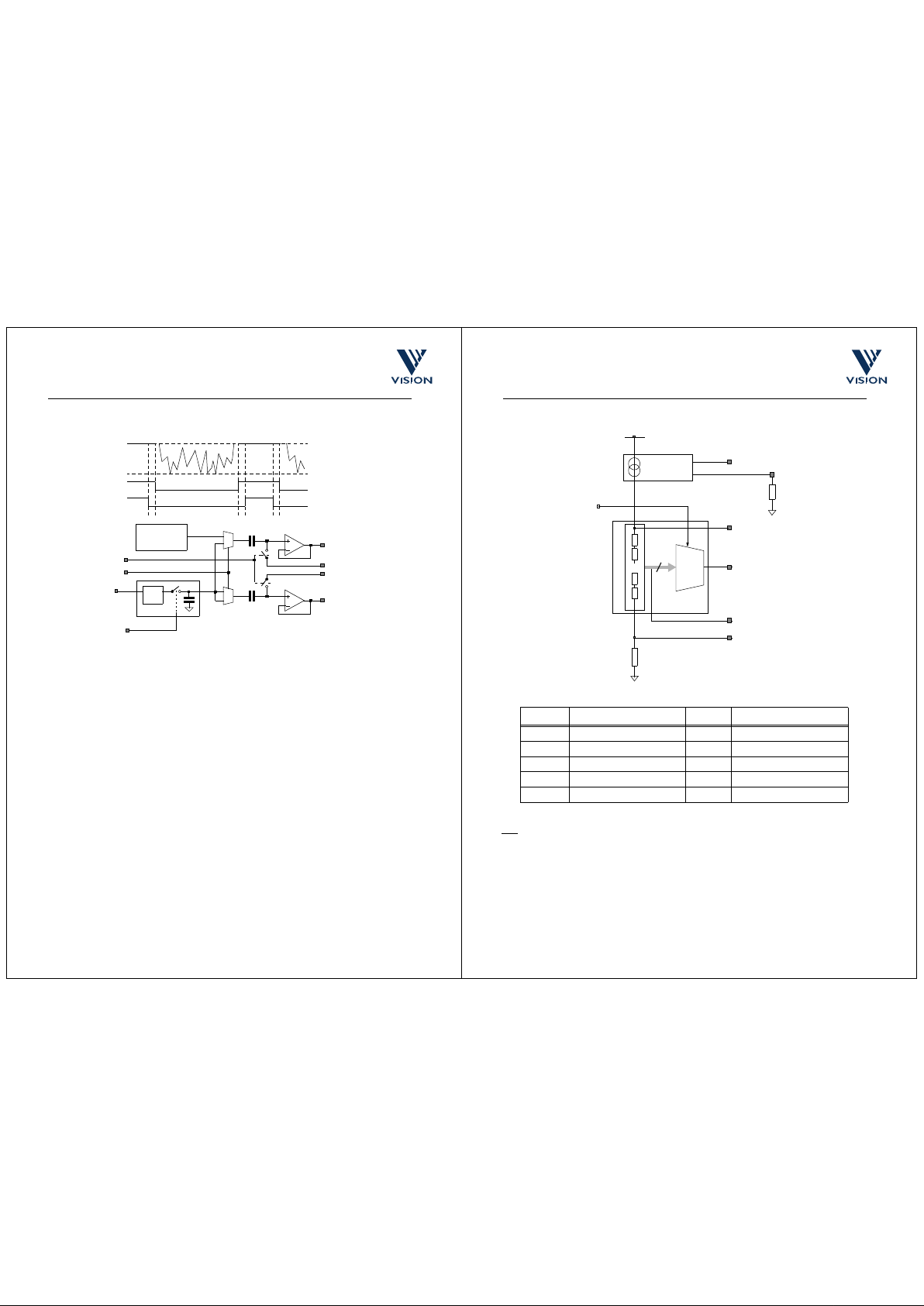
The resetting and reading of pixels is performed on a line by line basis, that is a row of column amplifiers
reads a whole line of pixel voltages in parallel. The reset/integrate/read cycle for a line of pixels is controlled
by the Reset Vertical and Read Vertical shift registers (VSRs).
The length of the ‘Frame Integrate’ pulse, FI, propagating along the Reset Vertical shift register sets the pixel
integration time. FI going high at a point along the VSR releases that line of pixels from RESET, starting the
integration period. The two-line ‘Frame Read’ pulse, FR, which comes at the end of the integrate period,
starts the field readout, which proceeds from ‘bottom’ to ‘top’. As FR propagates along the Read Vertical shift
register, it controls which line is to be read. For exposure control by means of a shutter mechanism, FI should
be held high throughout the frame integrate/read cycle.
The Vertical Shift Registers are clocked by the Line Clock pulse, LCK. Within a frame, first an even line, then
an odd line is read. This is controlled by the EVEN clock, which must be h alf th e LCK frequency and change
two PCKs before LS (Line Start) rises. A pair of lines may be ‘skipped over’ (for example as in ‘Horizontal
Cine’ mode—See Section 2.3), by inserting two LCK pulses and one EVEN pulse between line readout
sequences. .
Figure 2.2 : Relative timing for single frame integration and readout
Note: If FR does not rise with the rising edge of EVEN, that is if EVEN is high duri n g th e second line period
of the FR pulse, the AVO-valid line readout sequence is offset by one line.
Further control of the VSRs is effected by: VCLRB (Clear Reset and Read); VSETB (preset Reset to ones);
CDSR (reset row, but do not advance VSRs). The PXRD input to the Read VSR enables a line of pixels to
be read out. (See Section 5. and Section 7.5 for more details.)
The first six lines in the array are black reference lines. The reset/integrate cycle for these lines is controlled
by a third shift register, defined by bits CR[4] and CR[3] in the Control Register (See Section 6.). This shift
register can either hold the black reference lines in permanent reset, allow minimum exposure or have the
same int egration time (e xposure) as the rest of the ar ray.
The readout sequence, initiated by FR going high, is therefore: six black lines followed by eight colour
characterisation lines, 2 ‘dummy’ line, 1280 valid video lines, 2 further ‘dummy’ lines, eight further colour
characterisation lines.
With any of the three ‘Vertical Cine’ modes enabled, the six black reference lines are always read out, but
the rest of the array is subsampled (subsampling commences with the colour characterisation lines at the
bottom of the array), e.g. with Vertical Cine enabled to carry out
1
/2 subsampling (see Section 5.4.2), this
becomes: six black lines, four colour characterisation lines, 2 dummy lines, 640 valid video lines, and a further
four colour characterisation lines.
Note
: ‘Vertical Cine Mode’ is a new feature on the VV6801. On the VV6850/5850, this feature is not available,
therefore line skipping timing schemes would be required to achieve the same vertical subsampling effect as
Vertical Cine Mode provides on the VV6801/5801. See Section 5.4.2 and Section 6.5.
LCK
FI
FR
EVEN
AVO
Valid Video Line
Black Ref LineAVO Not Valid
1306 Lines
Exposure
cd24082b.fm 09/09/98: PRELIMINARY 8
VISION VV6801/5801 PRELIMINARY CUSTOMER DATASHEET Rev 1.1
Pr
e
l
i
mi
na
ry
2.3 Horizontal Shift Register
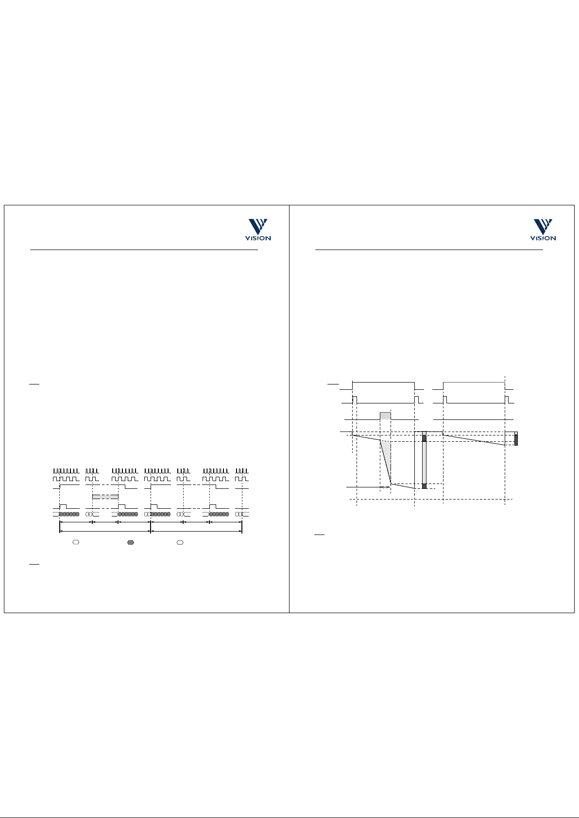
The Horizontal Shift Register is clocked by the Pixel Clock, PCK. Columns are read out, from left to right, by
the Line Start pulse, LS, propagating along the Horizontal Shift Register. The LS pulse must be four PCK
periods long, with the first valid pixel being sampled after the falling edge (see Section 7. for exact
relationship). To avoid bandwidth limitations within the output stage causing cross talk problems between the
colours in a colour pixelated sensor, the horizontal shift register either reads out the odd or the even columns,
under control of the EC signal.
In order to read valid pixel data, the Pixel Read input to the Read VSR, PXRD, must be pulsed high, as shown
in Figure 2.3. When reading out either the even columns (EC=1) or the odd columns (EC=0) it is the central
512 pixels of the 514 pixels read out that are valid. In Horizontal Cine mode (Selected with bit CR[3] in the
Control Register), every second pixel within a row is read out; of the 258 pixels read out for either EC=1 or
EC=0, the central 256 pixels are valid. To preserve the correct aspect ratio, Vertical Cine mode can be
enabled to skip every second line pair, as shown in Figure 2.4.
Note
: ‘Horizontal Cine Mode’ on VV6801/5801 performs the same function as ‘Cine Mode’ on the VV6850/
5850.
Figure 2.3 : Relative line readout timing (Full Resolution)
Figure 2.4 : Relative line readout timing (Horizontal Cine Mode and
1
/2 Vertical Cine
mode enabled)
The HCLRB input (active low) clears the HSR to all zeros. HCLRB can also be used, for example,
to prematurely end a line scan, perhaps when only part of the image is req uired.
Note:
The power-on reset signal, RSTB, can be used to drive HCLRB (and VCLRB for the Vertical
Shift Registers) at pow er up.
PXRD
LCKLSEC
EVEN
Even line
Odd Line
AVO
Even pixels
Odd pixels
Even pixels
Odd pixels
PXRD
LCKLSEC
EVEN
Even line (0)
Odd Line (1)
Even line (4)
AVO
Even
Odd
Even
Odd
Even
Odd
Odd
Line (5)
Sensor timing skips two lines
Page 5
cd24082b.fm 09/09/98: PRELIMINARY 9
VISION VV6801/5801 PRELIMINARY CUSTOMER DATASHEET Rev 1.1
Pr
e
l
i
mi
na
ry
2.4 Pixel Readout Architecture
Figure 2.5 : Pixel Readout Schematic
2.5 Video Output
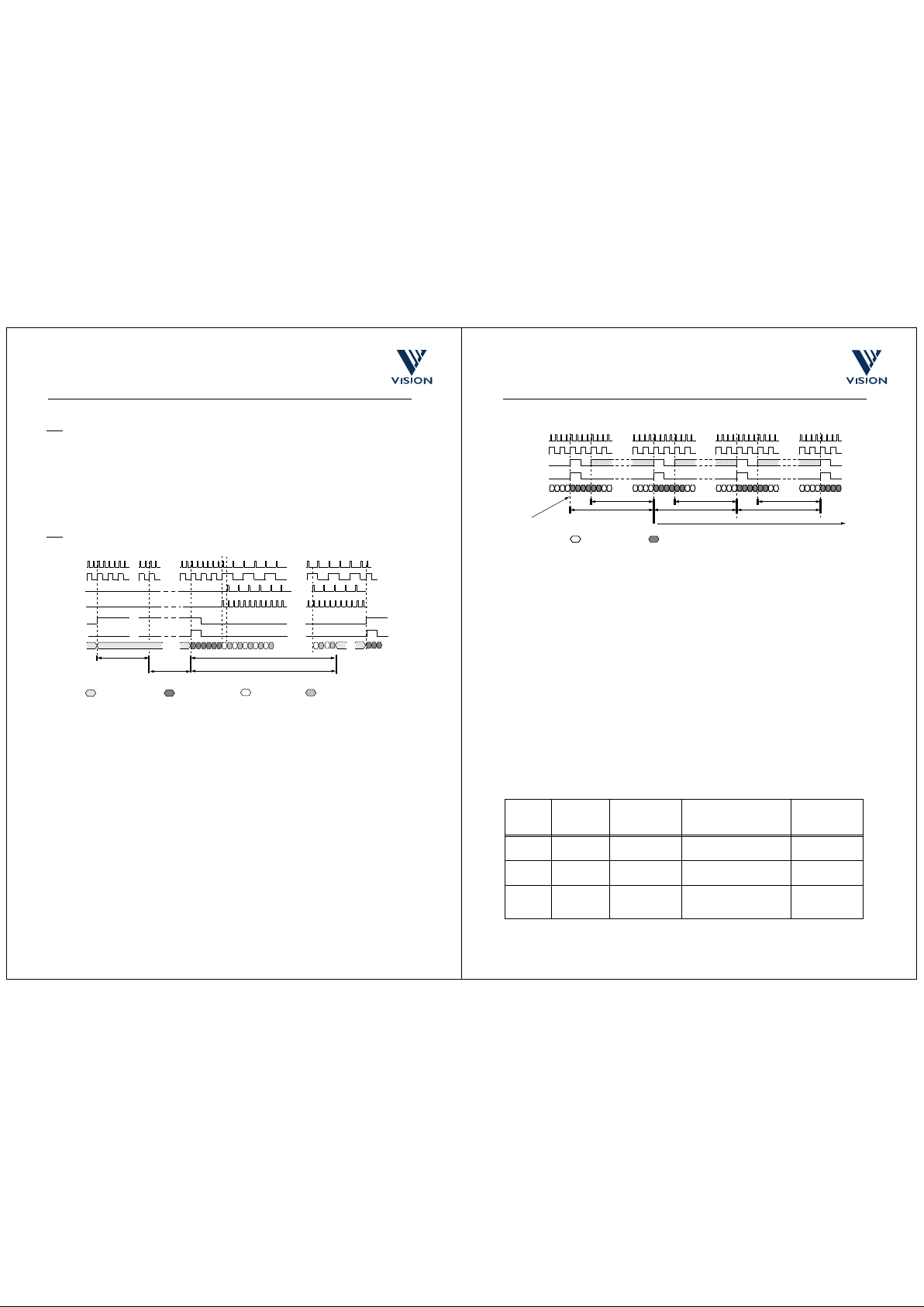
The four-PCK long LS pulse initiates output of a line of video, with the first valid pixel being sampled after LS
bit-line, Vx[m]
Pixel Array
AVO
PCK
Reset[n]
Horizontal Shift Register
D
pix
Bitline Test/Clamp Circuitry
HCLRB
VRT
Read[n]
CR[0]
Vbltw
CR[1]
C
pix
CS[m]
LS
CS[401:0]
Output Channel 0
Output Channel 1
Output
Stage
CSo[401:0]
CSe[401:0]
EC
COLsam
Output Channel 2
Output Channel 3
EC
VRT
SAMRef
Line Reference
AVORef
Output
Channel
Clamp
SELRef
CLAMP
HCINE
VRT
Read[m]
Read Vertical Shift Register
Reset Vertical Shift Regist er
FR
FI
LCK
VSETB
VCLRB
PXRD
EVEN
Vbloom
CDSR
Sample/Hold
Source Follower
Column[m]
Sample/Hold circuit
Pixel[m,n]
cd24082b.fm 09/09/98: PRELIMINARY 10
VISION VV6801/5801 PRELIMINARY CUSTOMER DATASHEET Rev 1.1
Pr
e
l
i
mi
na
ry
falls, and subsequent pixels appearing at AVO as LS propagates along the Horizontal Shift Register. The
AVO output for each pixel should then be sampled as close to the end of the PCK cycle as possible to allow
maximum settlin g tim e.
Figure 2.6 : Pixel Level Sampling
2.6 The Video Output Chain
At the top of each column of the array is a sample and hold stage (controlled by COLsam), which drives the
output stage. The purpose of the sample & hold is to ensure that all the pixels in a line have the same
exposure, as the outputs of a row of pixels are sampled at the same instant. If COLsam is not used then each
pixel will carry on integrating until it is read out. Therefore, since all pixels within a line are released from reset
at the same time, each pixel will have a different integration time, and hence exposure value.
The columns are read out via four output channels. Each channel is multiplexed onto the AVO pin via an AC
coupling stage to restore the DC content. The AVORef pin provides a pseudo-differential output, obtained
from an internal black reference. (The pseudo-differential output stage cancels out leakage across the
coupling capacitors since both output channels experience the same rate of decay.)
Note
: The video at AVO is ‘inverted’, that is Black is higher than White.
2.7 AVO Reference
The DC content of the output stage is set by using the SELRef signal to simultaneously put the internal
reference on the AVO and AVORef output channels, and then the CLAMP signal to charge the amplifier side
of the coupling stages to VCL1 and VCL2 respectively. The integrated 5-bit DAC, controlled by Control
Register bits CR[15..11], can be used to adjust one or other of these clamping voltages. The CLAMP signal
must fall before SELRef falls. The AC Coupling Capacitors must be refreshed at least once every still image
capture sequence, or every frame of a live video.
LS
PCK
AVO
AVO output has settled
PCK [R]
changes pixel
PCK [R]
Samples LS
First Valid pixel after
LS is sampled
on AVO
¼ PCK max. @ 5MHz
Page 6
cd24082b.fm 09/09/98: PRELIMINARY 11
VISION VV6801/5801 PRELIMINARY CUSTOMER DATASHEET Rev 1.1
Pr
e
l
i
mi
na
ry
Figure 2.7 : Analogue output circuit
The sensor’s internal black reference, which drives the AVORef output path, is derived from a separate 8 by
8 array of pixels connected in parallel. The input voltage to all pixels in the 8 by 8 array is VRT, that is the
pixels are in reset. A sample & hold stage controlled by SAMRef allows the VRT voltage driving the black
reference pixels to be sampled, freezing the black reference value.
Normally the black level reference should be updated between every still im age c aptur e sequenc e or
between every frame in live video mode. Under very high illumination, however, the black reference should
be sampled between every line in live video mode.
The internal black reference can be sampled at the beginning of a frame using SAMRef. It can also be
observed line by line by asserting SELRef (without CLAMP) in the dead period between reading rows of
pixels out onto AVO.
2.8 The 5-Bit DAC
The internal five bit resistive ladder DAC is energised by a Bias Generator that is set by the internal Bandgap
Voltage Reference, Vbg, and the external 12K resistor connected from Rset to AGND. The Vdac output of
the DAC, which can be used to set either VCL1 or VCL2, is adjusted by bits 11 to 15 of the Control Register/
AVO
SELRef
White
Black
Peak
CLAMP
AVO
VCL2
VCL1
CLAMP
AVORef
VRT
8x8
Pixels
SAMRef
Pixel Array
+ Columns
Black Reference
SELRef
2:1
cd24082b.fm 09/09/98: PRELIMINARY 12
VISION VV6801/5801 PRELIMINARY CUSTOMER DATASHEET Rev 1.1
Pr
e
l
i
mi
na
ry
Serial Interface.
Figure 2.8 : 5 bit DAC
Note: The Vbg pin is a high impedance output, and can be over-ridden within the VCL input limits.
2.9 Black Reference Lines
There are six lines at the bottom of the pixel array that are covered with opaque masking. These black
reference lines have their own reset shift register. A four to one multiplexer, controlled by Control Register
bits CR[4] and CR[3], selects the input to this shift register (FBCK), and hence the operating mode. The four
modes of operation are:
1. Permanent Reset - By setting FBCK low, the black lines are permanently reset to VRT.
2. Minimum Integration - FBCK follows the field read pulse, FR; the black reference lines are held in minimum exposure.
3. Integration - FBCK follows the field read pulse, FI; the black reference lines therefore have the same
Parameter Definition Value Comment
Vdactop 208/122 * V bg 2.08V
Vdacbot 176/122 * Vbg 1.76V
Vdac3/4 199/122 * Vbg 1.99V
Vdac CR[15..11] * (32/122 * Vbg) Zdac Vdac Output Impedance 21K Ohms ±25%
Table 2.1 : 5-Bit DAC Parameters
32
Analogue
Vdac
CR[15..11]
Resistive Ladd er, 32R
AGND
Vdacbot
Vdactop
Vdac3/4
176R
AVCC
I = Vbg/122R
R ~ 100 Ohms
12K
Vbg
Mux(32:1)
Bias
Generator
Rset
5-Bit DAC
Page 7

cd24082b.fm 09/09/98: PRELIMINARY 13
VISION VV6801/5801 PRELIMINARY CUSTOMER DATASHEET Rev 1.1
Pr
e
l
i
mi
na
ry
exposure time as the array.
4. Permanent integration; the reference lines continue to integrate until reset as in 1.
2.9.1 Permanent Reset
This is the most stable as it does not depend on either the quality of the black shield above the black pixels
or any light incident on the pixels. However it is also the least accurate as it does not allow for dark current
or the breakthrough of the falling edge of the pixel reset signal onto the pixel capacitance. The resulting
reference value will be ‘blacker’ than black due to the above errors.
2.9.2 Minimum Integration
This is more accurate than Permanent Reset, as the effect of the pixel reset signal breakthrough is included,
but the effect of total dark current is not included since the black reference pixels are not integrating for the
same time as the image section of the pixel array. The reference is, also, now sensitive to the effects of light
reaching the black line pixels.
2.9.3 Integration
This includes the effect of dark current since the black reference pixels are integrating for the same time as
the image section of the pixel array. The validity of the reference is, however, now even more sensitive to the
effects of light reaching the pixel.
2.9.4 Permanent integration
This, in combination with Permanent Reset, allows the exposure time for the black reference lines to be
controlled independently of the exposure of the rest of the image.
Note: For best results, it is recommended that the average of the four central lines of the black reference line
group is used to characterise ‘Black’ for the frame.
cd24082b.fm 09/09/98: PRELIMINARY 14
VISION VV6801/5801 PRELIMINARY CUSTOMER DATASHEET Rev 1.1
Pr
e
l
i
mi
na
ry
3. Exposure Control
Exposure control is achieved either electronically by varying the FI pulse duration, or directly by means of a
shutter arrangement (mechanical, electro-mechanical, electro-optical, and so on). The correct exposure level
for any scene can be assessed by processing a ‘trial exposure’ of the scene, or by utilising the ‘Accumulate’
or ‘Parallel Integration’ operating mode. See Section 5. for a full description of exposure control.
Page 8

cd24082b.fm 09/09/98: PRELIMINARY 15
VISION VV6801/5801 PRELIMINARY CUSTOMER DATASHEET Rev 1.1
Pr
e
l
i
mi
na
ry
4. Removing Noise
There are many possible ways achieve FPN cancellation in order to produce the highest quality stills images
from the VV6801 sensor. The exact method chosen will depend on the intended use of the imager system,
and the ancillary devices available in the system, such as the frame buffer and mechanical shutter typical of
a Digital Stills Camera. A number of schemes are discussed.
In order to obtain high quality, low noise images from the VV6801 sensor pixel to pixel offset variations, or
Fixed Pattern Noise (FPN), must be removed. This can be done by reading the image array more than once,
for example reading in the dark to establish a reference for each pixel, then reading the exposed array to
collect ‘image plus offset’ data, then subtracting to remove the offsets. To obtain the lowest noise operation
the random pixel ‘reset’ noise must also be removed.
4.1 Sources of Fixed Pattern Noise
The major sources of Fixed Pattern Noise in the sensor that can be cancelled are:
• Transistor Threshold Offsets
• Dark Current
Each of the above can be effectively cancelled to a much lower residual random noise level by using the
techniques described below. The residual noise sources in the sensor, such as flicker noise, dark current shot
noise, thermal noise and ADC Quantisation noise, that cannot be cancelled, or are a function of the
cancellation techniques, define the overall camera noise performance.
4.2 Methods of Removing Fixed Pattern Noise
4.2.1 Transistor Threshold Offsets
Each pixel amplifier, each column source follower and each output channel multiplexer, has a unique offset
caused by process variations in the threshold voltage of the transistors. This offset is independent of
exposure, and will be relatively stable with respect to temperature and operating conditions.To remove
Transistor Threshold FPN, the VV6801 is used in conjunction with an ADC and either a frame buffer or a line
buffer:
•
Pixel offset removal frame by frame with a shutter:
A frame buffer is used to obtain the pixel to pixel
DC offsets for the whole image. The offsets are obtained by capturing a dark (FPN) frame with the
shutter closed, and an ‘image’ frame with the shutter open. The ‘clean’ image data can then be extracted
by subtraction. (This technique can only be used with a physical shutter, and with at least one extra dark
frame acquisition period.)
•
Pixel offset removal frame by frame with a reference frame:
A non-volatile frame buffer is used to
obtain the pixel to pixel DC offsets for the whole image at camera build. These offsets are then
subtracted from the exposed ‘image’ as it is read to obtain the ‘clean’ image data. (This technique gives
the fastest frame acquisition time at the expense of accuracy.)
•
Pixel offset removal line by line:
A line of pixel information is read and stored in a line buffer. The line
is then reset to black using the CDSR signal, before being re-read to obtain the pixel to pixel DC offsets
for that line. As the line is re-read the offset data for each pixel is subtracted from the value stored in the
line buffer, the result being the ‘image’ data. (The COLsam signal must be used to ensure that samples
in the same line have the same integration period.)
With line by line offset removal the time for reading out a complete frame is doubled, since each line has to
be read twice. It is also not possible to remove pixel reset noise or dark current, thus there is a trade off
between the frame readout rate and image quality, and the amount of memory required.
Full frame offset removal can be achieved in many ways, depending on what ancillary devices are available
in the camera system, and constraints such as image quality required and acceptable minimum frame
readout rate.
4.2.2 Dark Current
The ‘dark current’ in a pixel photodiode is the inherent leakage that discharges the integrating capacitance
in the same way as incident light. Hence, Dark Current FPN builds up on the array whenever the array is
cd24082b.fm 09/09/98: PRELIMINARY 16
VISION VV6801/5801 PRELIMINARY CUSTOMER DATASHEET Rev 1.1
Pr
e
l
i
mi
na
ry
released from reset, that is when FI is high. This means that the amount of dark signal depends on exposure
time, and varies from pixel to pixel.
The same degree of dark current charge build-up occurs in the array whether or not the array is exposed to
light. Therefore, if the array is allowed to integrate (FI high) with no incident light for the same length of time
as for the image exposure, the dark current element of the exposed image data can be ascertained and
removed from the image data by subtraction, leaving behind the dark current shot noise.
Since dark current also depends on temperature the dark frame should be taken close in time to the image
frame, in order to avoid ambient temperature variations.
4.2.3 ‘Reset Noise’ Cancellation
One random noise source that can be cancelled is ‘reset noise’ (or ‘kTC’ noise), which is due to the switching
of the photodiode capacitance when the pixel is released from reset. This is present in all subsequent reads
of the array (without reset) to the same extent. These can therefore be extracted by reading the array
immediately after reset (when FI goes high) and subtracting the value obtained from the ‘exposed’ array data.
This operation also cancels Pixel Threshold Offsets.
To achieve reset noise cancellation, FR should be taken high for two LCK periods when FI goes high, and
1306 lines read
before
the array is exposed to the required image. The pixel data from this pass of FR through
the VSRs must be stored in a frame buffer, and subtracted from the exposed image data. The exposed image
is obtained when FR is pulsed high again, coincident with the last two LCK periods of FI being high after the
exposure period.
It is not possible to describe all of the many operating schemes that can be devised for image capture and
FPN reduction. The basic recommended modes for camera operation are described in Section 5., with
detailed timing requirements in Section 7.
Page 9
cd24082b.fm 09/09/98: PRELIMINARY 17
VISION VV6801/5801 PRELIMINARY CUSTOMER DATASHEET Rev 1.1
Pr
e
l
i
mi
na
ry
5. Operating Modes
There are six main operating modes for the sensor:
1. Still Image Capture with a Frame Buffe r
2. Correlated Double Sampling (line by line FPN cancellation)
3. Live-Video Mode
4. Subsampled Mode (Horizontal and Vertical ‘Cine’ modes)
5. Parallel Integration
6. Accumulate
These are explained in the following sections, together with detailed timing requirements for the various
control signals necessary to operate the sensor. An additional suggested mode of operation (‘Multiple Dark
Current Periods’) is explained in Section 5.7.
5.1 Still Image Capture with a Frame Buffer
This is the recommended operational mode for high quality still image capture in camera systems where
there is an electro-mechanical shutter in front of the sensor and a Frame Buffer for temporary image storage.
FPN cancellation is central to this mode of operation, and is described in detail. Other operational schemes
that may be devised can include all or some of the techniques employed in this example, but the elements
are essentially the same. (See Section 5.7 for a discussion of variations to this FPN cancellation scheme.)
Note
: For the simplest possible image capture mode, with no FPN cancellation, see the description of the
Vertical Shift Registers above.
The basic still image capture cycle starts with the shutter closed. The array is released from reset by taking
the input to the reset vertical shift registers, FI, high. The system controlling the camera must then wait for
1306 lines to allow this “integrate wavefront” to propagate through the shift register, before opening the
shutter. When FI goes high FR should also be pulsed high for 2 lines to initiate the Read sequence. Reading
each pixel as soon as it is released from reset yields a reset image which contains both the fixed pattern noise
component for each pixel and the random reset noise due to that particular reset operation. This image
should be stored in a frame buffer.
When the shutter has closed after exposure FR must be pulsed high again for 2 lines to re-read the array and
obtain the exposed image data. Again, it will take 1306 lines to read all of the array pixels. FI should fall when
FR falls, to return the active pixel array into reset. As the image frame is read out the appropriate pixel reset
value, as stored in the frame buffer, is subtracted from the current pixel value and the result written to the
frame store. This removes both pixel reset noise and pixel to pixel DC offsets from the image.
Figure 5.1 : Relative timing of still image capture with frame buffer
Note: See Section 7. for exact relationships.
Due to the length of time taken to read out an image (200 ms, assuming a 5 MHz clock rate), the dark current
in each pixel is a significant part of the image data. To remove the fixed pattern noise injected by the dark
current a ‘dark image’ must be captured with the same integration time as the exposed image but with the
shutter closed. Subtracting the dark image from the exposed image removes the dark current fixed pattern
LCK
FI
1306 Lines
FR
EVEN
AVO
T1=Exposure
Integrate=T
1
1306 Lines 1306 Lines
1306 Lines
Image Frame Dark Current Frame
Valid Video Line Black Ref Line AVO Not Valid
Shutter
cd24082b.fm 09/09/98: PRELIMINARY 18
VISION VV6801/5801 PRELIMINARY CUSTOMER DATASHEET Rev 1.1
Pr
e
l
i
mi
na
ry
noise, leaving a ‘clean’ image. This process can be summarised as follows:
1. With the shutter closed, release the sensor from reset and immediately read a frame into the buffer
memory; this captures the array threshold FPN and reset noise (‘V
Reset
’)
2. After 1306 line periods, open the shutter and expose the sensor to the required scene (the exposure
time can be determined by ‘Parallel Integration’ or ‘Accumulate’ — see below)
3. Close the shutter and immediately read the array; as each pixel is read, subtract the value for that position stored in the frame buffer, and overwrite that pixel location with the difference — the memory now
contains the image plus dark current FPN (V
im
+ V
Dark
)
4. After the 1306 line periods of the second read, repeat the image capture cycle, but do not open the
shutter; this time, load a
second
frame buffer with first the V
Reset
value and then the V
Dark
value (after
subtraction)
5. After the second integration period, subtract the V
Dark
value for each pixel that is stored in the second
frame buffer from the (V
im
+ V
Dark
) value for that position stored in the first frame buffer and overwrite
that pixel location with the result.
The frame buffer now contains the corrected image values, which can be processed for colour and so on,
then transferred to permanent image storage memory.
The pixel voltages for this method are illustrated schematically below:
Figure 5.2 : Pixel voltages during still image capture with frame buffer
Note: Since the ‘integrate wavefront’ must propagate through the VSR, the point at which the open shutter
exposure occurs will vary progressively from line to line of the array — from close to ‘Read2’ on the bottom
line to close to ‘Read1’ at the top.
5.2 Correlated Double Sampling (line by line)
This is an alternative FPN cancellation mode for camera systems where there is only a Line Buffer available
for temporary image capture, and not necessarily a mechanical shutter in front of the sensor. The method
outlined below, using the CDSR signal, relates to a still image capture in a shuttered camera system, but the
same principle could also be applied to exposure control with the FI pulse duration in Still Fr am e and Liv e
Reset[n]
Read[n]
V
pix
VRT
V
Black
V
White
V
Reset
Read 2
Read 4
V
Dark1Vim
V
Dark1
Shutter
Exposure
Not to scale
V
Dark2VDark2
+
+
Image
Read 1
Read 3
V
Dark
= V
Dark1
+ V
Dark2
Page 10
cd24082b.fm 09/09/98: PRELIMINARY 19
VISION VV6801/5801 PRELIMINARY CUSTOMER DATASHEET Rev 1.1
Pr
e
l
i
mi
na
ry
Video modes.
Note
: This method does not cancel dark current FPN, and as the pixel is reset twice, has two lots of ‘reset’
noise sources.
The array is released from reset by taking the input to the reset vertical shift registers, FI, high. The system
controlling the camera must then wait for 1306 lines to allow this “integrate wavefront” to propagate through
the shift register, before opening the shutter (or further extending the FI pulse). After the sensor has been
exposed for the appropriate time, FR must be pulsed high for 2 lines to read the pixel array and obtain the
exposed image data, which is loaded into the Line Buffer line by line.
When a line of 1028 pixels of image data has been read, the CDSR signal is pulsed high to reset the line of
pixels to Black (without advancing the HSR). COLSam is then pulsed to resample the row, and as each pixel
is read out this ‘Black Offset’ value is subtracted from the value stored in the line buffer and the result passed
on as corrected image data.
Note
: During the 1280-line image data readout, LCK and EVEN must be at least twice their minimum periods
(with maximum PCK rate of 5.0MHz), to allow for the second line read.
Figure 5.3 : Relative timing for Correlated Double Sampling (CDS)
(See Section 7.5 for the exact relationships, and also how CDSR, COLSam and PXRD should interact.)
5.3 Live-Video Mode
In the ‘Live Video’ mode the effect is similar to a conventional video camera, with a frame readout rate of just
under five frames/second (with a 5 MHz pixel clock) at full resolution. This could be used, for example, to
provide a moving ‘viewfinder’ display for a stills camera, however for achieving faster frame readout rates,
see Section 5.4.
In Live-Video mode the exposure level for a frame is controlled electronically by varying the high duration of
the FI waveform. The high duration of FI can be varied from 2 lines (minimum exposure) in multiples of 2 lines
up to 1306 lines (maximum exposure). The falling edge of FI is fixed within the fra me, the refore it is the
leading edge of FI that must be moved to vary exposure.
The field read pulse, FR, must be set high for the 2 lines preceding the falling edge of FI; this means that the
FR waveform is identical to the FI waveform for minimum exposure. The necessary signal relationships are
LCK
FI
1306 Lines
FR
EVEN
AVO
Exposure
1306 Lines
Read ImageBlack Ref LineAVO Not Valid
Read Black Offset
CDSR
Read Image & Offsets
COLsam
cd24082b.fm 09/09/98: PRELIMINARY 20
VISION VV6801/5801 PRELIMINARY CUSTOMER DATASHEET Rev 1.1
Pr
e
l
i
mi
na
ry
illustrated below:
Figure 5.4 : Relative timing of Live Video mode
If a frame buffer is being used to store the pixel to pixel DC offsets the first image captured on entering LiveVideo mode should have minimum exposure to obtain and store pixel offset data. However, if the offset data
already exists in memory this step is not required.
5.4 Cine Modes
‘Cine’ mode is similar to ‘Live Video’ mode, since it continuously integrates and reads the array, but achieves
higher frame readout rates by subsampling the image both vertically and horizontally. Both Horizontal and
Vertical subsampling can be enabled in sensor timing.
5.4.1 Horizontal Cine Mode
Selecting Horizontal Cine mode via the Serial Data Control Register (CR[2]) subsamples the pixels in a line,
reading out only every other pixel pair. (See Section 2.3 for details.) Horizontal Cine mode enables higher
frame readout rates to be achieved, particularly when used in conjunction with Vertical Cine Mode.
For high frame readout rates, it is also best to read a dark f rame into memory and subtract the F i xed Pattern
Noise as the array is read in order to reduce the frame overhead of either line-rate CDS or the Shuttered
Frame-rate cancellation schemes.
5.4.2 Vertical Cine Mode
This feature simplifies the timing requirements for vertical subsampling by removing the requirement to skip
lines through timing generation (which was necessary with the VV6850/5850). 3 hardwired subsampling
modes are available:
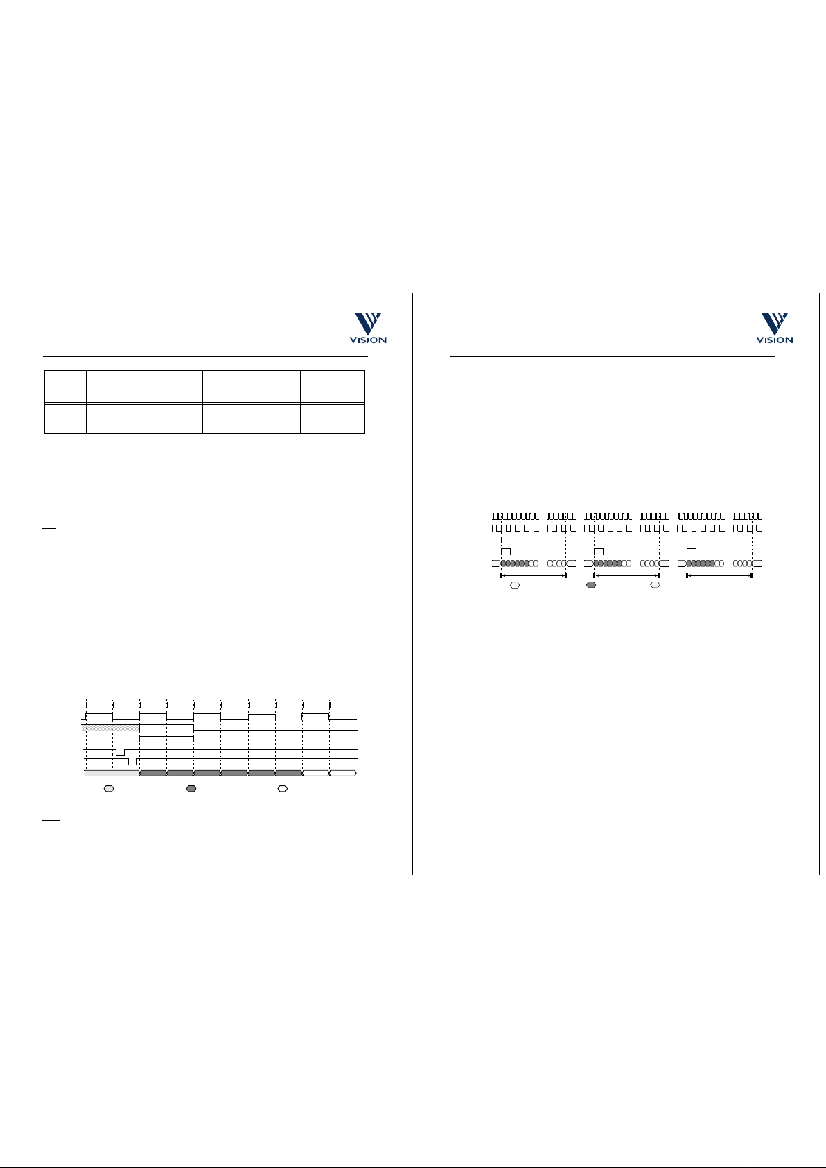
CR[18:17]
Vertical
Subsampling
Effect Final viewfinder resolution
Max. frame
readout rate
@10MHz PCK
00 None None 1280 x 1024 (Horizontal Cine
Mode disabled)
6.24/sec
01 1/2 Skip every 2nd
line pair
640 x 512 (With Horizontal
Cine Mode)
21/sec
10 1/4 Skip 3 line pairs in
every 4
320 x 256 (With Horizontal
Cine Mode and external pixel
subsampling)
42/sec
LCK
FI
1306 Lines (1 Frame)
FR
EVEN
AVO
Exposure
Exposure
Read Pixel Offsets
Live-Video Frames
Valid Video Line
Black Ref Line
1306 Lines (1 Frame)
1306 Lines (1 Frame)
Exposure
Page 11
cd24082b.fm 09/09/98: PRELIMINARY 21
VISION VV6801/5801 PRELIMINARY CUSTOMER DATASHEET Rev 1.1
Pr
e
l
i
mi
na
ry
When 1/2 vertical subsampling is used in conjunction with Horizontal Cine mode, a viewfinder image of 640
x 512 pixels will be produced with the correct aspect ratio. When 1/4 or 1/8 vertical subsampling is used, an
incorrect aspect ratio will be read out from the sensor, since Horizontal Cine Mode only permits 1/2
subsampling, however pixel pairs can be skipped in software/post processing to regain the correct aspect
ratio.
Although additional external horizontal subsampling is still required to regain the correct aspect ratio for a 1/
4 or 1/8 subsampled viewfinder, enabling Horizontal Cine mode is still advantageous, since it will speed up
sensor readout: one line period will require 740 PCK cycles rather than 1252 (see Section 7.5.2).
Note
: Line skipping schemes other than the those available may be desirable for certain applications where
the vertical subsampling ratio is a non integer power of two (e.g. 1/3 vertical subsampling). In these cases,
line skipping can be generated in external timing, as would be required when vertically subsampling the
VV6850/5850, where no vertical Cine mode is available.
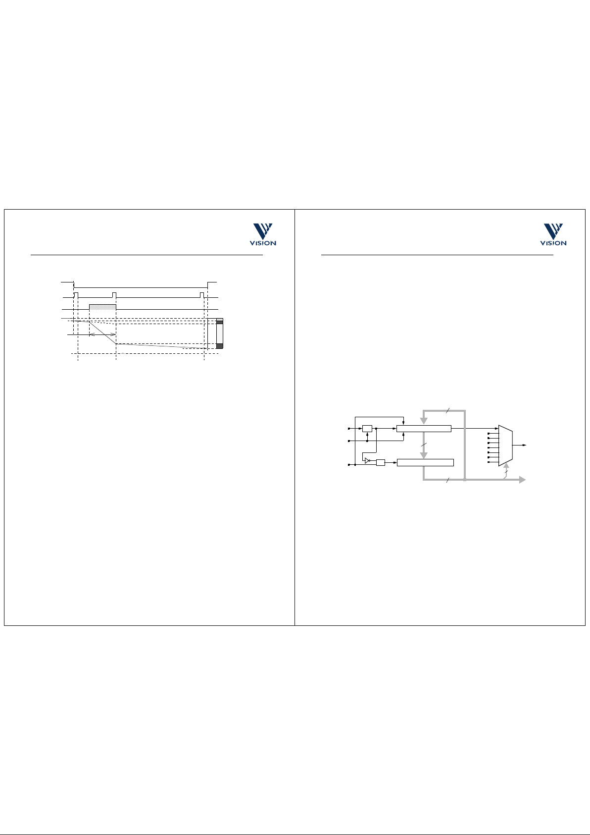
5.5 Parallel Integration
In this mode all of the pixels in the array are released from reset at the same time. This is achieved using the
VCLRB and VSETB signals for the vertical shift registers. (VSETB only effects the rese t sh i ft register). This
can be used to give a quick but crude estimate of correct exposure by, for example, counting lines until a line
is reached where all pixels in the line are saturated, then setting exposure to, say, 50% of the integration time
taken to reach that line.
The sequence of operations is as follows:
1. Pulse VCLRB low to reset the Read and Reset vertical shift registers to all zeros; this forces all pixels
into reset
2. Pulse VSETB low, this loads the Reset shift register with all ones, which starts all of the pixels integrating.
3. Then FR should be pulsed high for 2 lines to start the array readout.
Figure 5.5 : Relative timing for Parallel Integration Mode
Note:
VCLRB and VSETB must NEVER be taken low at the same time .
Since all pixels start to integrate at the same time and readout is sequential (line by line), each line of pixels
represents a different exposure value. If the FR pulse occurs on the next video line after VSETB goes high
11 1/8 Skip 7 line pairs in
every 8
160 x 128 (With Horizontal
Cine Mode and external pixel
subsampling)
84/sec
CR[18:17]
Vertical
Subsampling
Effect Final viewfinder resolution
Max. frame
readout rate
@10MHz PCK
Table 5.1 : Vertical Cine Mode
Valid Video LineBlack Ref LineAVO Not Valid
LCK
FI
FR
EVEN
AVO
VSETB
VCLRB
cd24082b.fm 09/09/98: PRELIMINARY 22
VISION VV6801/5801 PRELIMINARY CUSTOMER DATASHEET Rev 1.1
Pr
e
l
i
mi
na
ry
then the first valid video line readout will have been exposed for 6 lines (the black reference lines), and the
last line of valid video will have been exposed for 1306 lines.
5.6 Accumulate
In ‘Accumulate’ mode the pixel array is repeatedly re-read without resetting the pixels. This mode is intended
for exposure monitoring in conjunction with a flash when light levels are low, and more than one frame time
is required to obtain sufficient integration.
The array is released from reset by taking FI high. At the same time FR is pulsed high for 2 lines to read out
the pixel reset values. Then at the required intervals (of not less than 1306 line periods) FR is pulsed high for
2 lines to re-read the array. While the array is being repeatedly re-read FI must stay high. Effectively, the
successive reads of the array are monitoring the rate of charge accumulation in the pixels.
When sufficient integration has occurred to produce, say 50% average saturation, reading can be terminated.
The number of frames of exposure required to achieve this can then be used to calculate the flash energy
required to correctly expose the scene. On the falling edge of FR for the final array read, FI should go low, to
return the pixel array into reset.
Figure 5.6 : Relative timing for Accumulate mode
5.7 Multiple Dark Current Periods
This is a suggested modification to the noise cancellation sequence described in Section 5.1, to suit particular
application requirements, by extending the post image exposure ‘dark image’ capture period to some integral
multiple of the image exposure period, in order to obtain a more accurate assessment of the dark current
FPN:
1. With the shutter closed, release the sensor from reset and immediately read a frame into buffer ‘A’
memory; this captures the array threshold FPN and reset noise (‘V
Reset
’)
2. Open the shutter and expose the sensor to the required scene
3. Close the shutter and immediately read the array; as each pixel is read, subtract the value for that position stored in the frame buffer to obtain the image plus dark current FPN (V
im+VDark1
) value; store this
value in
second
frame buffer, ‘B’
4. After a further (say) four frame periods, read the array again; as each pixel is read, subtract the reset
value for that position as stored in the ‘A’ frame buffer, and overwrite the position, leaving the V
im
+
V
Dark1
+ V
Dark2
value in the buffer
5. For each pixel, subtract the value in ‘B’ from that in ‘A’ to give V
Dark2
dark current value, which is equiv-
alent to four times the V
Dark1
value
6. Divide the V
Dark2
values in ‘A’ by 4, then subtract them from the (Vim + V
Dark1
) values in ‘B’ and store
the result, which is the V
im
image data
The frame buffer now contains the corrected image values, which can be transferred to image storage
Valid Video Line
Black Ref Line
AVO Not Valid
LCKFI1306 Lines
FR
EVEN
AVO
1306 Lines
1306 Lines
Page 12
cd24082b.fm 09/09/98: PRELIMINARY 23
VISION VV6801/5801 PRELIMINARY CUSTOMER DATASHEET Rev 1.1
Pr
e
l
i
mi
na
ry
memory. This scheme is illustrated below :
Figure 5.7 : Multiple dark frame periods explanation
Reset[n]
Read[n]
V
pix
VRT
V
Black
V
White
Read 1
V
Reset
Read 2 Read 3
V
Dark1
V
im
V
Dark2
Shutter
Exposure
Not to scale
cd24082b.fm 09/09/98: PRELIMINARY 24
VISION VV6801/5801 PRELIMINARY CUSTOMER DATASHEET Rev 1.1
Pr
e
l
i
mi
na
ry
6. The Control Register & Serial Communication
The VV6801 includes a full duplex serial interface, and can be controlled and configured by a host processor.
Data describing the current configuration of the camera is stored in a 20-bit control register. This register can
be read from the camera on the serial interface, and can also be written to from the serial interface to change
camera operation.
6.1 General description
When a 22-bit serial interface data word arrives at the camera on DIN, the first 20 (msb) bits are loaded into
a shift register, and the last two bits (‘R/W’) are examined to ascertain if a ‘read’ operation or a ‘write’
operation is required. If a ‘write’ is required (‘R/W’ = “00”) the contents of the input shift register are t ransferred
to the control register. Otherwise, the current contents of the control register is output on DOUT. (Note: In
‘test mode’, that is with CR[7..5]>0, certain other signals are monitored by DOUT and CR[19..0] is not
transmitted.)
The signals used to effect the serial data interface are:
• DINSerial Data In; DIN is sampled on the rising edge of DCK
• DOUTSerial Data Output
• DCKSerial Data Clock
• DLATSerial Data Latch; transfers the input data word to the control register (for ‘write’),
and initiates control register output on DOUT (for CR[7..5]=0)
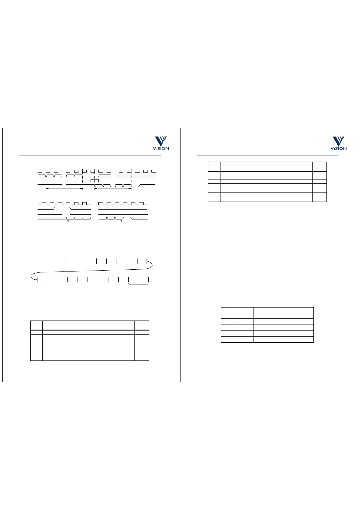
Figure 6.1 : Control register block diagram
6.2 Serial Communication Protocol
The host must perform the role of a communications master, while the camera acts as a slave receiver and
transmitter. Communication from host to camera takes the form of a 22-bit data word, with a 20-bit data word
returned to the host. Since the serial clock (DCK, maximum frequency 100kHz,) is generated by the host, the
host determines the data transfer rate.
The host sends the 20 bit control word, most significant bit first, then either holds DIN high for two clock
cycles, to indicate a ‘read’, or holds DIN low for two clock cycles, to indicate a ‘write’. The host also takes
DLAT high for one clock cycle, corresponding to the last bit of the R/W pair. This defines the end of the
transfer and latches the data word to the Control Register, if required (R/W=00). DLAT also (on the next rising
edge of DCK) transfers the contents of the Control Register to the Shift Register, which is then output to
DOUT if CR[7..5] = 0.
The data transfer protocol is illustrated below:
20-bit Shift Register
Control Register CR[19..0]
DIN
DCK
DLAT
DOUT
R/W20CR[19..0]20203CR[7:5]
8 to 1 Multiplexer
&
Page 13
cd24082b.fm 09/09/98: PRELIMINARY 25
VISION VV6801/5801 PRELIMINARY CUSTOMER DATASHEET Rev 1.1
Pr
e
l
i
mi
na
ry
Figure 6.2 : Serial data transfer protocol
6.3 The Serial Data Word
Figure 6.3 : Read Data Format
The 22-bit Serial Data Word consists of the two-bit wide R/W flag, and the 20 bits of Control Register data
(CR[0..19].
6.4 Register description
The following tables defines the CR information contained in the messages:
CR
Bit
Function/Comment Default
0 Bit-line Test Enable 0
1 Bit-line Clamp Enable 1
2 Select Horizontal ‘Cine’ mode: Only every second pixel pair is out-
put - i.e. every second pixel from each colour channel.
0
4,3 Controls the integration mode for black reference lines 0
7..5 Selects the node that DOUT is monitoring 0
8 Enables the Sample & Hold circuits on the four output channels 0
DLAT
DCK
DIN
DOUT*
CR[19]
* Only valid when CR[7:5] = 000 (Default)
DIN
DOUT*
Control Register Read Timings:
Control Register Write Timings:
CR[18] CR[0]CR[1]
CR[19] CR[18] CR[0 ]CR[1]
20 DCK Cycles
20 DCK Cycles
CR[19] CR[18] CR[0]CR[1]
DLAT
DCK
CR[2]CR[17]
20 DCK Cycles
D[4]
Read = 11
D[3] D[ 2] D[1] D[0]SWCP
SWCP
RSHOCLE
HCINE BLECLE R / WBM[0]BM[1]OS[0]OS[1]OS[2]
CR[19]
CR[0]
CR[9]
CR[8]
The 22-bit Serial Data Word (msb first)
VCINE[0]VCINE[1]
Reserved
cd24082b.fm 09/09/98: PRELIMINARY 26
VISION VV6801/5801 PRELIMINARY CUSTOMER DATASHEET Rev 1.1
Pr
e
l
i
mi
na
ry
6.5 Control Register Definitions
The various bits in the Control Register define operating modes and parameters as follows:
6.5.1 CR[0] - Bit-line Test Enable
Enables testing of the pixel column interconnections. This bit should always be 0.
6.5.2 CR[1] - Bit-Line Clamp Enable
The default is the bit-line clamp enabled, CR[1] = 1, which ensures that if a bit-line goes too low due to a pixel
being heavily over-exposed, the bit-line is clamped to Vbltw-Vtn.
Note:
Due to internal variations, the absolute clamp voltage will vary from column to column. Thus, care must
be taken to ensure that the ADC value clips before the bit-line clamp circuits operate otherwise column to
column fixed pattern noise will appear in the saturated white reg ions of the imag e.
6.5.3 CR[2] - Horizontal Cine Mode
Setting CR[2] = 1 forces the horizontal shift register to read out every second red, green or blue pixel in each
odd and even field. In this mode 258 pixels instead of 514 pixels are read out per colour per line. (Note: The
buffer columns on the left and right side of the pixel array are always read out, therefore the central 256 pixels
are valid for each colour channel.)
CR[8] and CR[16] should also both be low for Horizontal Cine mode.
6.5.4 CR[4:3] - Black Reference Line Integration Mode Select
CR[4] and CR[3] control the selection of the four possible integration modes to the black reference lines. The
Table below defines the code associated with each of the four modes.
(See Section 2.9 for details of these modes.)
6.5.5 CR[7:5] - Select DOUT output
Output to the DOUT pin is multiplexed under the control of CR[7], CR[6] and CR[5] for test purposes. All three
of these bits must be set to zero for image data to be observed on DOUT.
9 Connects the four black reference output channels together; the
default is AVORef cycling through the four channels
0
10 Enable clamping circuitry on the four output channels 1
15..11 D[4..0] - 5-bit Resistive DAC value; D[4] is msb 16
16 Switch in the Output Stage Sample&Hold Capacitors 0
18..17 Vertical Cine Mode select - subsample vertically 0
19 Reserved 0
CR[4] CR[3]
Integration Mode for Black reference
Lines
0 0 Permanent Reset.
0 1 Minimum Integration (FR)
1 0 Same integration time as main array (FI)
1 1 Always integrating.
CR
Bit
Function/Comme nt Default
Page 14
cd24082b.fm 09/09/98: PRELIMINARY 27
VISION VV6801/5801 PRELIMINARY CUSTOMER DATASHEET Rev 1.1
Pr
e
l
i
mi
na
ry
6.5.6 CR[8] - Output Channel Sample & Hold Enable
The sample and hold circuits in the AVO and AVORef output stages isolate the capacitive back injection
which occurs when an output channel is multiplexed onto the AC Coupling capacitor, which changes the
nature of the back injection:
Without sample and hold (CR[8] = 0 (default)), the interaction of the back injection and the column output
results in the AVO overshooting slightly before settling to the desired value
With sample and hold enabled (CR[8] = 1) the overshoot is eliminated, but the current pixel value will contain
a very small contribution from the previous pixel value read out on AVO
Note:
CR[16] allows the output channel sample /hold capacitor to be isolated from the signal path.
6.5.7 CR[9] - Common Up the Black Reference Channels
There are two options for operating the four black reference output channels:
1. CR[9]=0 : Operate with the AVORef cycling between each of the four black output channels. AVORef
will follow the shape of AVO as the AC coupling capacitor is cycling in the same way within both output
stages. Any mismatch between the black reference output channels will appear as a four-cycle pattern
on AVORef.
2. CR[9]=1 : Parallel up the operation of the black output channels. AVORef represents the average of the
four black output channels.
6.5.8 CR[10] - Output Channel Clamp Enable
Setting CR[10] = 1 (default) clamps the four output channels that are multiplexed onto AVO to prevent them
going beyond the designed operating voltage range. This ensures that each output channel always has
enough time to recover from being inactive before outputing pixel data.
6.5.9 CR[15:11] - 5-Bit Resistive DAC Data Value (D[5:0])
Data for the internal 5-bit Resistive Ladder DAC (default = 16). CR[15] is the MSB. See Section 2.8.
6.5.10CR[16] - Switch in Output Stage Sample/Hold Capacitors
Setting CR[16] high isolates the output channel sample/hold capacitors from the signal path. By isolating
these capacitors the output channels settle to the desired value in a shorter time.
Note:
CR[16] should only be set high when the output channel sample/holds are disabled.
The primary use of this function is in Cine mode. In this mode only two of the four output channels are in use.
As the two output channels have only half the time to settle, compared with the normal readout sequence,
CR[16] should be set high to improve settling of the output channels.
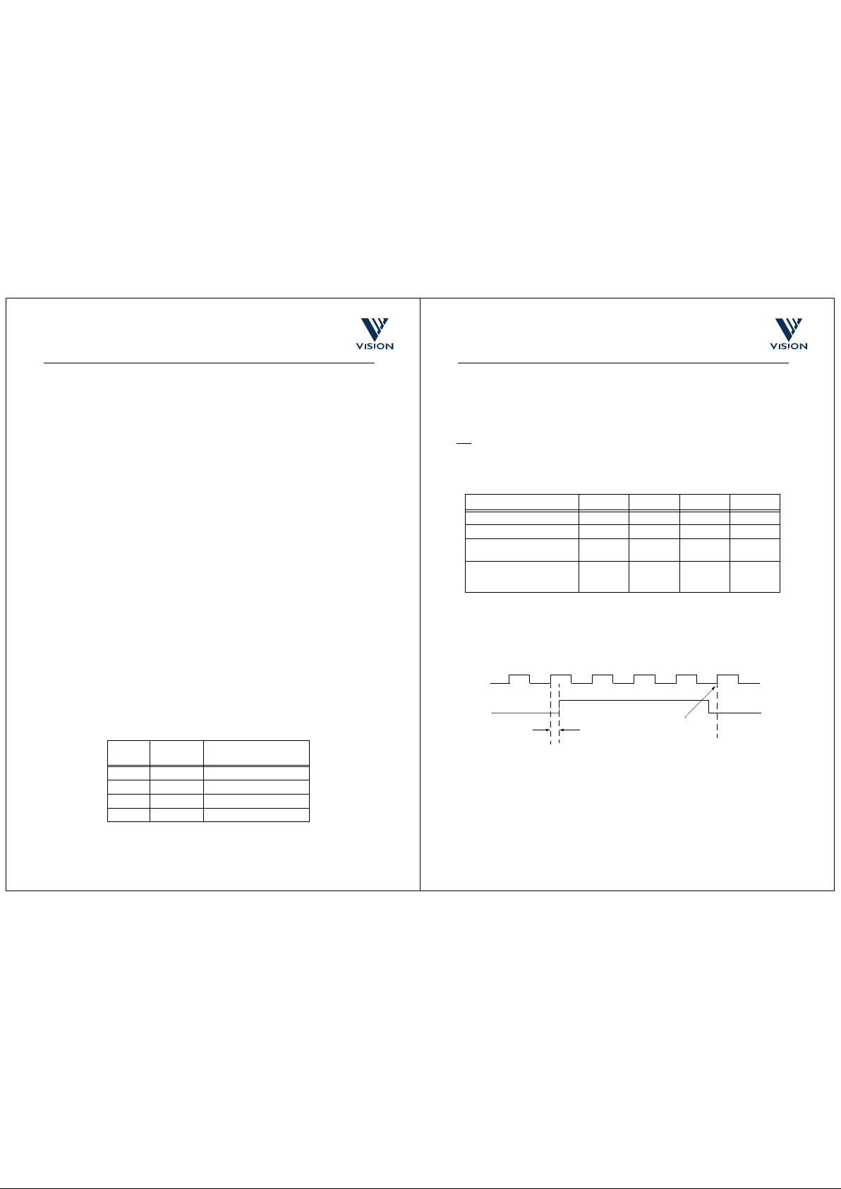
6.5.11CR[18:17] - Vertical Cine Modes
3 hardwired subsampling modes are available. This simplifies the timing requirements for vertical
subsampling by removing the requirement to skip lines through timing generation. See also Section 5.4
CR[18:17]
Vertical
Subsampling
Effect
00 None None
01 1/2 Skip every 2nd line pair
10 1/4 Skip 3 line pairs in every 4
11 1/8 Skip 7 line pairs in every 8
Table 6.1 : Vertical Cine Mode
cd24082b.fm 09/09/98: PRELIMINARY 28
VISION VV6801/5801 PRELIMINARY CUSTOMER DATASHEET Rev 1.1
Pr
e
l
i
mi
na
ry
7. Detailed Operational Timing
The following Section describes in detail the recommended timing for the primary operating modes. There
are many possible timing schemes, with more flexible setup and holds, but the recommended timings are
safe. Specifically, timing diagrams and tables are given for:
• Normal Array Read
• Correlated Double Sampling (line by line)
Note
: The timings in Section 7.1 to Section 7.5 have been expressed for a 5MHz PCK. The symbols
[T],[R],[F],[H],[L] signify Transitional edge, Rising edge, Falling edge, High Level and Low Level respectively.
7.1 System Clocks
Line and pixel timing is done in PCK’s, and all signals should change on the falling edge of PCK.
7.2 Line Start to PCK Timing
The relative timing of the Line Start pulse, LS, and the Pixel Clock, PCK, is extremely important for correct
sensor operation. LS must be set up at least 20ns after the rising edge of PCK, no later than (PCK Period)/
4 after the rising edge of PCK, and must be held for four PCK cycles. This is illustrated below:
Figure 7.1 : Line Start to PCK Timing
7.3 Initial Power Up Timing
On powering up the array should be reset by VCLRB and HCLRB, to help the settling of the internal
references. An internal power-on-reset circuit generates RSTB, which can be used to reset the sensor.
The references VRT and Vbg must be stable before the first frame; this will be a function of the decoupling.
The internal reference and AC coupling stages should be put into sample mode by making SELRef, SAMRef,
and CLAMP high.
To ensure that the array is inactive until the first frame on power up FI, FR, LS, PCK, LCK and EVEN should
Min Typ Max Units
PCK Period 100 200 - nS
PCK Duty Cycle 40 - 60 %
Line Period 1252 (for full
line readout)
1252 - PCK’s
Line Period (HCINE Mode) 740 (for full
subsampled
line readout)
740 - PCK’s
Table 7.1 : System Clocks.
LS
PCK
PCK [R]
changes pixel
on AVO
min:
20ns
max: (PCK Period )/4
Page 15
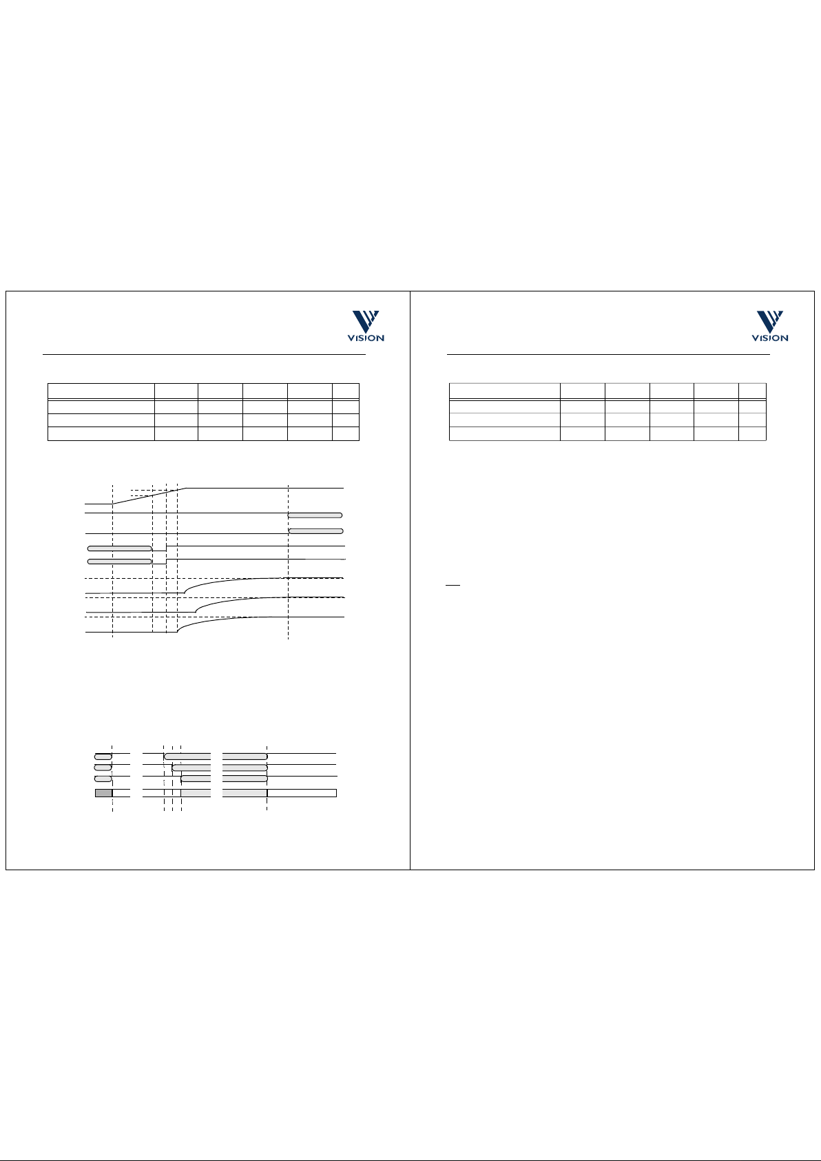
cd24082b.fm 09/09/98: PRELIMINARY 29
VISION VV6801/5801 PRELIMINARY CUSTOMER DATASHEET Rev 1.1
Pr
e
l
i
mi
na
ry
all be low.
Figure 7.2 : Startup timing sequence
Note:
Serial Data can only be sent after RSTB rises.
7.4 Inter-Frame Timing
When a frame is to be taken, the first task is to sample the reference with SAMRef. This signal should be held
high until the first line, which should be for at least 100uS.
If possible, SAMRef should be held high between acquisition of still frames. In order to also ensure that the
AC coupling stages do not drift, SELRef and CLAMP should also be held high.
Figure 7.3 : Inter Frame Timings
Event Timing Min Typ Max Units
Power On Reset trigger Voltage PU1 - 2.7 - V
RSTB pulse width PU2-PU1 100 - - uS
Settling Ti me PU4-PU3 10 - - mS
Table 7.2 : Recommended Start-Up Timing.
VDD
FR/FI/LS
HCLRB/
VRT
Other References
VBG
VCLRB
RSTB
4.5V
2.7V
PU0 PU1
PU2
PU3
PU4
(RSTB should be used to drive HCLRB and VCLRB to reset the sensor)
SELRef/
SAMRef/
Power-up
First Frame
CLAMP
F0
SAMRef
CLAMP
SELRef
F1 F2 F3 F4
FRAME
Valid
Pixels
cd24082b.fm 09/09/98: PRELIMINARY 30
VISION VV6801/5801 PRELIMINARY CUSTOMER DATASHEET Rev 1.1
Pr
e
l
i
mi
na
ry
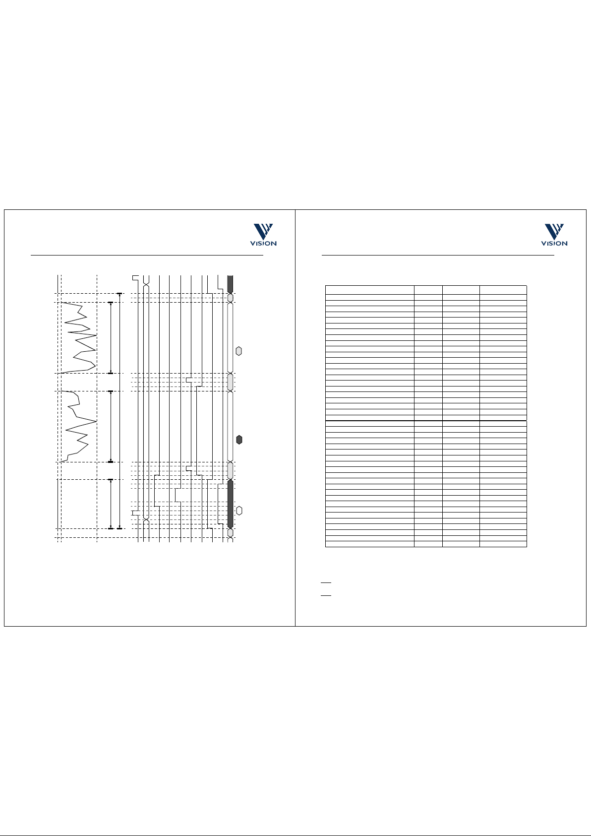
7.5 Line Read-Out Timing
The following diagrams and tables define the relative timings of the various control signals required to read
a line of pixels. Not all of the signals shown will be required for all modes of operation, but where they are
these timing constraints must be observed. Timings for Correlated Double Sampling (using CDSR) are given
after the standard line read definitions.
LCK is the master clock for the vertical shift registers, for reading and resetting rows. LCK is a latching signal,
and latches when high (to be reset on the next PCK).
The EVEN signal transitions must precede LCK, and FI & FR must straddle LCK. PXRD must be high when
COLSam is pulsed. EC & EVEN are not latched, and must therefore remain high while reading valid pixels.
The first line of pixel information is read out when the EVEN and FR signals are both high. If the EVEN signal
is high during the second line period of FR pulse, the line readout sequence will be offset by one line relative
to that outlined in the timing specification. This is due to the FR and FI inputs only being sampled when both
LCK and EVEN are high.
Note
: The recommended timings shown in Table 7.5 to Table 7.9 are
preliminary
and subject to change.
Event Timing Min Typ Max Units
SAMRef Period F1-F0 100 - - uS
CLAMP overlap of SAMRef[F] F2-F1 1 uS
SELRef overlap of CLAMP[F} F3-F2 0.200 uS
Table 7.3 : Inter Frame Timings
Page 16
cd24082b.fm 09/09/98: PRELIMINARY 31
VISION VV6801/5801 PRELIMINARY CUSTOMER DATASHEET Rev 1.1
Pr
e
l
i
mi
na
ry
Valid Video Data
AVO Reference Level
AVO Not Valid
Table 7.4 : Line Timings for Reading The Array
Black Level
Peak White
1 Line
l0
l2
l3
l4
l5
l6
l7
l8
l1
l9
l10
Reference Level
Even Columns (514 pixels) Odd columns (514 pixels)
PXRD
LCK
LS
EC
EVEN
SELRef
AVO
AVO
COLsam
CDSR
l11
l12
l13
l14
l15
l16
l19
l17
l18
CLAMP *
l20
l21
Reference Level
* CLAMP is only used if Line update of AC coupling is required in HCINE mode
cd24082b.fm 09/09/98: PRELIMINARY 32
VISION VV6801/5801 PRELIMINARY CUSTOMER DATASHEET Rev 1.1
Pr
e
l
i
mi
na
ry
7.5.1 Full Resolution (‘Live Video’/Still Image Capture) Modes
Table 7.5 : Recommended Line timings
Note: CLAMP is asserted only during the clamping line, in the case of frame rate clampling, or during every
line, in the case of line rate clamping.
Note
: All input signals should change on the Falling Edge of PCK, except LS (see Section 7.2).
Description #t PCK Cycles Time (us) @5MHz
SELREF [R] -Start of line c0 0 0
CLAMP [R] (See note) c1 1 0.2
EVEN [T] c2 0 0
LCK [R] c3 4 0.8
LCK [F] c4 5 1
PXRD [R] c5 34 6.8
COLSAM [R] c6 35 7
COLSAM [F] c7 204 40.8
CLAMP [F] c8 205 41
SELREF [F] c9 206 41.2
EC [R], PXRD[F] c10 207 41.4
LS [R] (even pixels) c11 208 41.6
LS [F] (even pixels) c12 212 42.4
AVO valid, even pixels start c13 212.5 42.5
AVO valid, even pixels end c14 726.5 145.3
EC [F] c15 728 145.6
LS [R] (odd pixels) c16 729 145.8
LS [F] (odd pixels) c17 733 146.6
AVO valid, odd pixels start c18 733.5 146.7
AVO valid, odd pixels end c19 1247.5 249.5
End of line c21 1251 250.2
SELREF [R] -Start of next line 1252 250.4
Setup times:
Line Length c21-c0 1252 250.4
EVEN[T] - LCK[R] setup time c3-c2 4 0.8
LCK duration c4-c3 1 0.2
LCK[F] - PXRD[F] c10-c4 202 40.4
PXRD[R] - COLsam[R] setup c6-c5 1 0.2
COLsam duration c7-c6 169 33.8
COLsam[R] - CLAMP [F] c8-c7 1 0.2
CLAMP[H] Duration c8-c1 204 40.8
SELRef[H] Duration c9-c0 206 41.2
SELRef overlap of CLAMP c1-c0,c9-c8 1 0.2
SELRef[F] - EC[R] c10-c9 1 0.2
COLsam[F] - EC[R] c10-c7 3 0.6
EC[T] - LS[R]: even c11-c10 1 0.2
EC[T] - LS[R]: odd c16-c15 1 0.2
LS[H] duration: even c12-c11 4 0.8
LS[H] duration: odd c17-c16 4 0.8
LS[F] to first valid even pixel c13-c12 0.5 0.1
LS[F] to first valid odd pixel c18-c17 0.5 0.1
Valid pixels: even c14-c13 514 102.8
Valid pixels: odd c19-c18 514 102.8
PXRD[F] - SELref[R] (next line) c21-c10 1044 208.8
Page 17
cd24082b.fm 09/09/98: PRELIMINARY 33
VISION VV6801/5801 PRELIMINARY CUSTOMER DATASHEET Rev 1.1
Pr
e
l
i
mi
na
ry
7.5.2 Horizontal Cine Mode (1/2 subsampled)
Table 7.6 : Recommended Line timings in Horizontal Cine Mode
Note: CLAMP is asserted only during the clamping line, in the case of frame rate clampling, or during every
line, in the case of line rate clamping.
Note
: All input signals should change on the Falling Edge of PCK, except LS (see Section 7.2).
Description #t PCK Cycles Time (us) @5MHz
SELREF [R] -Start of line c0 0 0
CLAMP [R] (See note) c1 1 0.2
EVEN [T] c2 0 0
LCK [R] c3 4 0.8
LCK [F] c4 5 1
PXRD [R] c5 34 6.8
COLSAM [R] c6 35 7
COLSAM [F] c7 204 40.8
CLAMP [F] c8 205 41
SELREF [F] c9 206 41.2
EC [R], PXRD[F] c10 207 41.4
LS [R] (even pixels) c11 208 41.6
LS [F] (even pixels) c12 212 42.4
AVO valid, even pixels start c13 212.5 42.5
AVO valid, even pixels end c14 470.5 94.1
EC [F] c15 472 94.4
LS [R] (odd pixels) c16 473 94.6
LS [F] (odd pixels) c17 477 95.4
AVO valid, odd pixels start c18 477.5 95.5
AVO valid, odd pixels end c19 735.5 147.1
End of line c21 739 147.8
SELREF [R] -Start of next line 740 148
Setup times:
Line Length c21-c0 624 124.8
EVEN[T] - LCK[R] setup time c3-c2 4 0.8
LCK duration c4-c3 1 0.2
LCK[F] - PXRD[F] c10-c4 202 40.4
PXRD[R] - COLsam[R] setup c6-c5 1 0.2
COLsam duration c7-c6 169 33.8
COLsam[R] - CLAMP [F] c8-c7 1 0.2
CLAMP[H] Duration c8-c1 204 40.8
SELRef[H] Duration c9-c0 206 41.2
SELRef overlap of CLAMP c1-c0,c9-c8 1 0.2
SELRef[F] - EC[R] c10-c9 1 0.2
COLsam[F] - EC[R] c10-c7 3 0.6
EC[T] - LS[R]: even c11-c10 1 0.2
EC[T] - LS[R]: odd c16-c15 1 0.2
LS[H] duration: even c12-c11 4 0.8
LS[H] duration: odd c17-c16 4 0.8
LS[F] to first valid even pixel c13-c12 0.5 0.1
LS[F] to first valid odd pixel c18-c17 0.5 0.1
Valid pixels: even c14-c13 258 51.6
Valid pixels: odd c19-c18 258 51.6
PXRD[F] - SELref[R] (next line) c21-c10 532 106.4
cd24082b.fm 09/09/98: PRELIMINARY 34
VISION VV6801/5801 PRELIMINARY CUSTOMER DATASHEET Rev 1.1
Pr
e
l
i
mi
na
ry
7.6 Line Timing using CDSR
The following timing details relate to Correlated Double Sampling on a line by line basis, that is using the
CDSR signal to reset a line of pixels without advancing the VSR. The image capture part of the double read
is exactly as described above, and all setup times and durations other than CDSR specific times are also
identical. See Section 5.2 for full details.
Valid Video Data AVO R efe ren ce Level AVO Not Valid
Table 7.7 : Line Timings for r ead ing pi xe l dat a and the black off set data using the CDSR signal
Black Level
Peak W hite
1 Line
c10
Reference Level
Even C olu mn s O dd columns
PXRD
LCK
LS
EC
EVEN
SELRef
AVO
AVO
CD SR
Reference
(514 pixels) (514 pixels)
Level
(514 pixels)
Black Offsets
Eve n C olu mn s
Pixel Data Pixel Data
CO Lsam
c0
c2
c3
c4
c5
c6
c7
c8
c1
c9
c11
c12
c13
c14
c15
c16
c17
c18
c19
c20
c21
c22
c23
c24
c25
c26
c27
c28
c30
c31
c32
c33
c34
c35
(514 pixels )
Black Offsets
Odd Columns
c36
c37
c29
Page 18
cd24082b.fm 09/09/98: PRELIMINARY 35
VISION VV6801/5801 PRELIMINARY CUSTOMER DATASHEET Rev 1.1
Pr
e
l
i
mi
na
ry
7.6.3 Additional timing for CDSR Full Resolution Modes
Table 7.8 : Recommended Line timings for CDSR
Note: All input signals should change on the Falling Edge of PCK, except LS (see Section 7.2).
Description #t PCK Cycles Time (us) @5MHz
SELREF [R] -Start of line c0 0 0
CDSR[R] c21 1256 251.2
CDSR[F] c22 1281 256.2
PXRD [R] c23 1286 257.2
COLSAM [R] c24 1287 257.4
COLSAM [F] c25 1456 291.2
EC [R], PXRD[F] c26 1459 291.8
LS [R] (even pixels) c27 1460 292
LS [F] (even pixels) c28 1464 292.8
AVO valid, even pixels start c29 1464.5 292.9
AVO valid, even pixels end c30 1978.5 395.7
EC [F] c31 1980 396
LS [R] (odd pixels) c32 1981 396.2
LS [F] (odd pixels) c33 1985 397
AVO valid, odd pixels start c34 1985.5 397.1
AVO valid, odd pixels end c35 2499.5 499.9
End of line c37 2503 500.6
Setup times:
SELREF [R] -Start of next line 2504 500.8
Line Length 2504 500.8
Valid EXPOSED pixels: even c14-c13 514 102.8
Valid EXPOSED pixels: odd c19-c18 514 102.8
Valid RESET pixels: even c30-c29 514 102.8
Valid RESET pixels: odd c35-c34 514 102.8
CDSR[H] duration c22-c21 25 5
cd24082b.fm 09/09/98: PRELIMINARY 36
VISION VV6801/5801 PRELIMINARY CUSTOMER DATASHEET Rev 1.1
Pr
e
l
i
mi
na
ry
7.6.4 Additional timing for CDSR Horizontal Cine Mode (1/2 subsampled)
Table 7.9 : Recommended Line timings for CDSR in Horizontal Cine Mode
Note: All input signals should change on the Falling Edge of PCK, except LS (see Section 7.2).
Description #t PCK Cycles Time (us) @5MHz
SELREF [R] -Start of line c0 0 0
CDSR[R] c21 744 148.8
CDSR[F] c22 769 153.8
PXRD [R] c23 774 154.8
COLSAM [R] c24 775 155
COLSAM [F] c25 944 188.8
EC [R], PXRD[F] c26 947 189.4
LS [R] (even pixels) c27 948 189.6
LS [F] (even pixels) c28 952 190.4
AVO valid, even pixels start c29 952.5 190.5
AVO valid, even pixels end c30 1210.5 242.1
EC [F] c31 1212 242.4
LS [R] (odd pixels) c32 1213 242.6
LS [F] (odd pixels) c33 1217 243.4
AVO valid, odd pixels start c34 1217.5 243.5
AVO valid, odd pixels end c35 1475.5 295.1
End of line c37 1479 295.8
SELREF [R] -Start of next line 1480 296
Setup times:
Line Length 1480 296
Valid EXPOSED pixels: even c14-c13 258 51.6
Valid EXPOSED pixels: odd c19-c18 258 51.6
Valid RESET pixels: even c30-c29 258 51.6
Valid RESET pixels: odd c35-c34 258 51.6
CDSR[H] duration c22-c21 25 5
Page 19
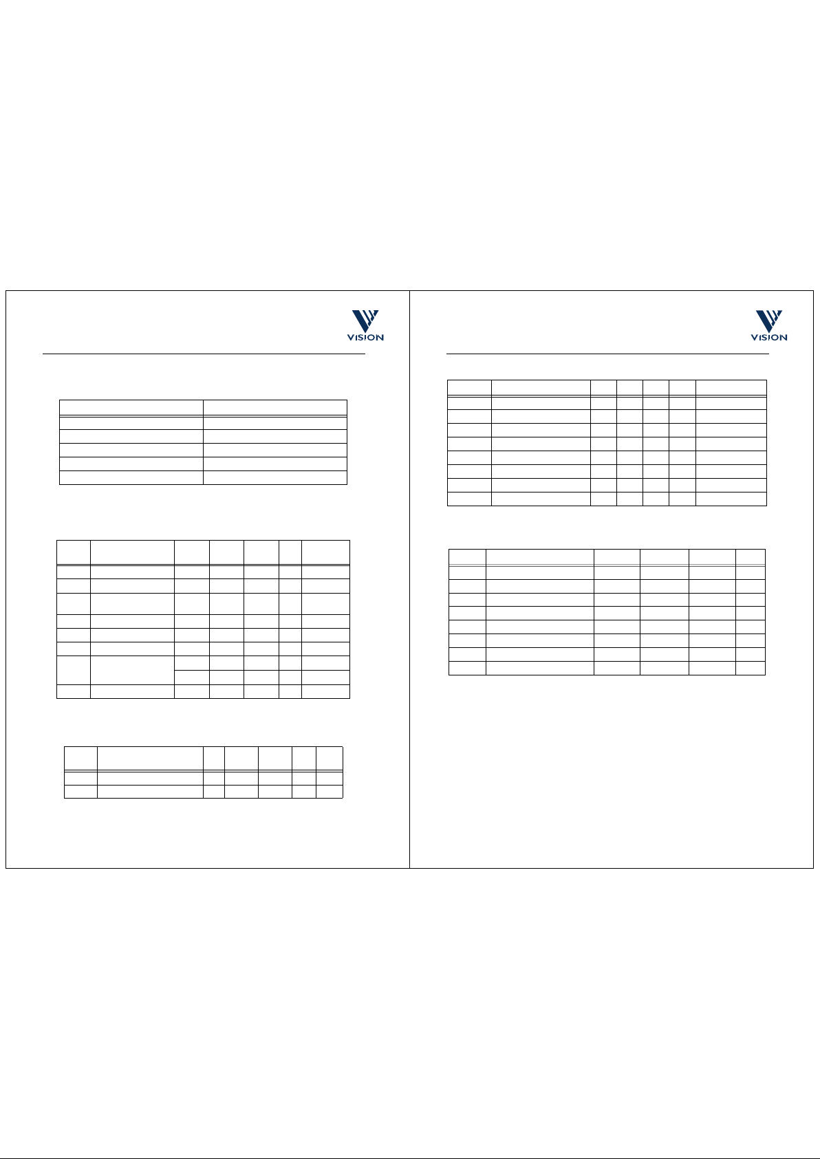
cd24082b.fm 09/09/98: PRELIMINARY 37
VISION VV6801/5801 PRELIMINARY CUSTOMER DATASHEET Rev 1.1
Pr
e
l
i
mi
na
ry
8. Detailed Specifications
8.1 Absolute Maximum Ratings
Note:
Stresses exceeding the Absolute Maximum Ratings may induce failure. Exposure to absolute
maximum ratings for extended periods may reduce reliabilit y . Fun ction alit y at or above these condit ions is
not implied.
8.2 DC Operating Conditions
Note 1.Digital and Analogue outputs unloaded.
Note 2: Allows control of sensor with 3v logic. To be confirmed.
8.3 AC Operating Conditions
Note 1. Recommended clock rate for 0.1% settling of AVO is 5.0MHz.
Note 2. Serial Interface clock must be generated by host processor.
Parameter Value
Supply Voltage -0.5 to +7.0 volts
Voltage on other input pins -0.5 to V
DD
+ 0.5 volts
Temperature under bias -15
o
C to 85oC
Storage Temperature -30
o
C to 125oC
Maximum DC TTL output Current Magnitude 10mA (per o/p, one at a time, 1sec. duration)
Symbol Parameter Min. Typ. Max.
Unit
s
Notes
V
DD
Operating supply voltage 4.75 5.0 5.25 V
I
DD
Overall supply cur rent
35 mA 1
V
IH
Input Voltage Logic “1” 1.5v
(note 2)
VDD+0.5 V
V
IL
Input Voltage Logic “0” -0.5 0.5 V
V
OH
Output Voltage Logic “1” VDD-0.5 V I=1mA
V
OL
Output Voltage Logic “0” 0.5 V I=1mA
I
ILK
Input Leakage cu rrent
-1
µ
A
VIH on input
1µA
VIL on input
C
load
Digital Input Cap. Load
10 pF
Symbol Parameter
Min
.
Typ. Max.
UnitsNote
s
PCK Pixel Clock frequenc y 5 10 MHz 1
DCK Serial Data Clock 100 KHz 2
cd24082b.fm 09/09/98: PRELIMINARY 38
VISION VV6801/5801 PRELIMINARY CUSTOMER DATASHEET Rev 1.1
Pr
e
l
i
mi
na
ry
8.4 Electrical Characteristics
8.5 Video Output Characteristics
Symbol Parameter Min. Typ. Max. Units Notes
VRTref Internal reference for VRT 2.85 3.0 3.15 V Unbuffered
VBLOOMref Internal reference for VBLOOM 1.90 2.0 2.10 V Unbuffered
VBLTWref Internal reference for VBLTW 1.35 1.50 1.65 V Unbuffered
V
BG
Internal bandgap reference 1.15 1.23 1.30 V Decoupl e with 0.1µ F
VCL1,2 Video Output Clamp Voltages 1.30 2.30 V An. Inputs
V
DAC
5-Bit DAC Output 1.76 2.08 V For VCL1 or 2
R
SET
Resistor to set DAC bias current -5% 12K +5% Ohms
I
VRT
Load Current on VRT 1.5 2.5 4 .0 mA Buffered from VRTref
Typical conditions, VDD = 5.0 V, TA = 25oC
Symbol Parameter Min. Typical Max. Units
V
black
AVO Black Level VCL1-30mV VCL1 VCL1 +30m V V
V
white
AVO Peak White - V
black
-1.0V - V
Pixel Reset to Pixel Reset -0.125 0 0.125 V
AVORef Pse udo-Diff. AVO Reference VCL2-30mV VCL2 VCL2+30mV V
I
AVO
AVO output current -2mA 4mA mA
F
AVO
AVO bandwidth 33MHz
C
AVO
AVO, AVOref Capacitive Loading 30 pF
R
AVO
AVO, AVOref Resistive loading 20K Ohms
Page 20
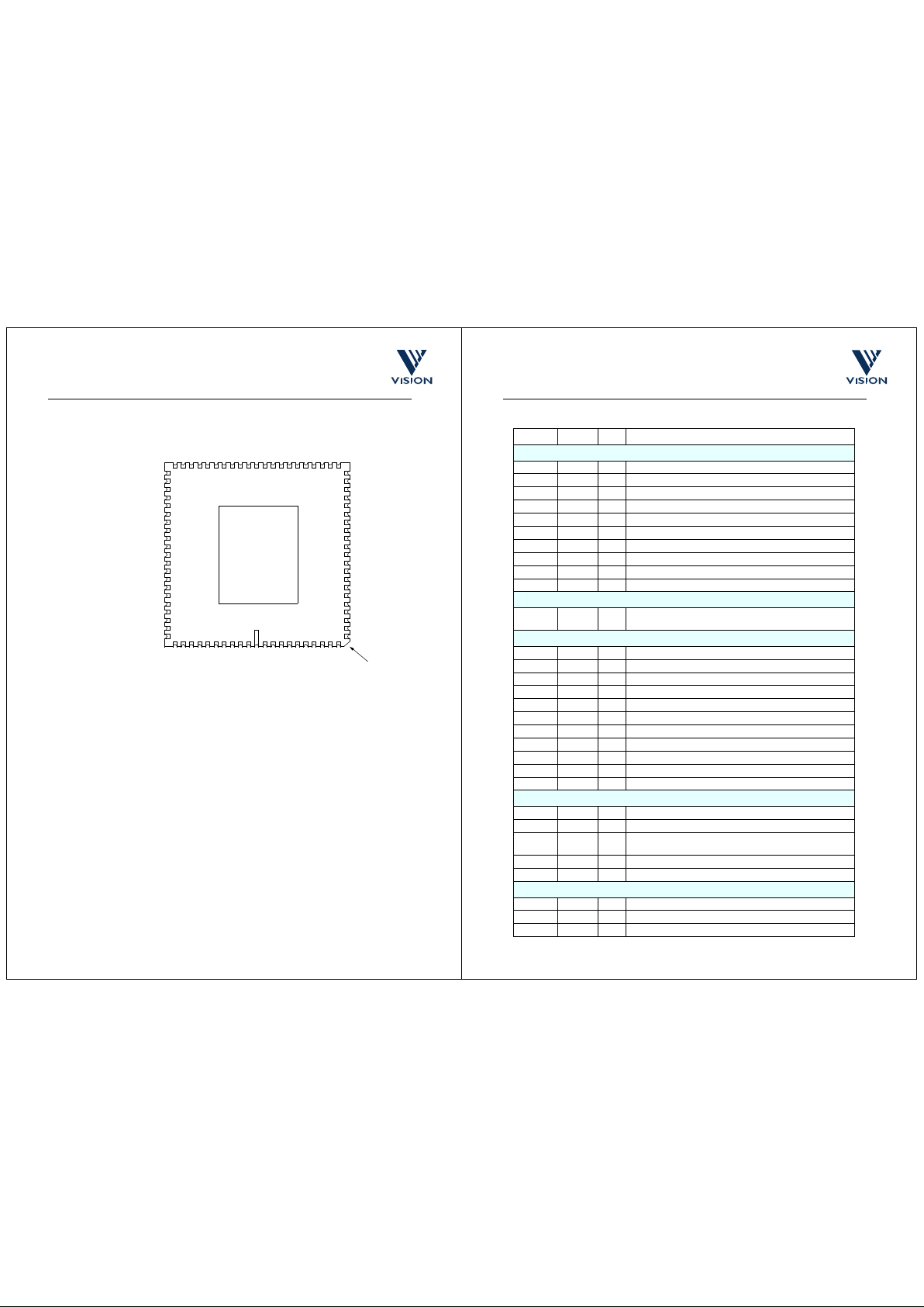
cd24082b.fm 09/09/98: PRELIMINARY 39
VISION VV6801/5801 PRELIMINARY CUSTOMER DATASHEET Rev 1.1
Pr
e
l
i
mi
na
ry
9. Pin descriptions and Package Details
Figure 9.1 : 84 LCC Pinout
For BGA pinout details, please contact VLSI VISION.
12345679 80 81 82 83 84
32
31
30
29
28
27
26
25
24
23
22
21
47 4 6 45 44 43 4253 52 51 50 49 48
54
55
56
57
58
59
60
61
62
63
64
65
AVDD2
Vdactop
VDiffRef
AVDD1
AVORef
AVSS1
AVO
Vdac
Vbltwref
Vdac
3/4
VCL2
VCL1
DVDD4
AGND1
AVCC1
DVSS4
SAMref
DOUT
LS
EC
COLsam
CLAMP
SELref
PCK
RSTB
DIN
DLAT
DCK
Viewed from top of package
35 34 3341 40 39 38 37 36
AGND2
AVCC2
DVDD3
DVSS3
66
67
68
69
70
71
72
73
74
HCLRB
EVEN
FR
FI
VSETB
VCLRB
PXRD
LCK
CDSR
18
17
16
15
14
13
12
20
19
AVCC3
Vblwt
AGND3
Vbg
Rset
Vnb
Vbloom
VRTref
Vblmref
75 7 6 77 78
DVSS1
DVDD1
VRT1
78910
VRT2
DVSS2
11
DVDD2
Index
‘TOP’
cd24082b.fm 09/09/98: PRELIMINARY 40
VISION VV6801/5801 PRELIMINARY CUSTOMER DATASHEET Rev 1.1
Pr
e
l
i
mi
na
ry
9.1 Pin List
Pin Name Type Function/Comment
POWER SUPPLIES
51, 35, 18 AVCC1-3 PWR 5V supply for the Column Source Followers.
50,36, 14 A GND1-3 GND Ground for the Substrate and the Column Source Followers.
28, 32 AVDD1,2 PWR 5V supply for the Output Stage.
30 AVSS1 GND Ground supply for the Output Stage.
75, 11 DVDD1,2 PWR 5V supply for Vertical Shift Registers
76, 10 DVSS1,2 GND Ground for Vertical Shift Registers
33 DVDD3 PWR 5V supply for Output Muxing.
34 DVSS3 GND Ground for Output Muxing.
53 DVDD4 PWR 5V supply for Horizontal Shift Register.
52 DVSS4 GND Ground for Horizontal Shift Register.
POWER-ON-RESET
65 RSTB OD Output of internal power-on-reset cell. Should be applied to
HCLRB and VCLRB at power up.
ANALOGUE VOLTAGE REFERENCES
77, 9 VRT1,2 IA Pixel Reset Voltage and Power Supply.
12 Vbloom IA A nti-bloomin g pixel reset voltage.
13 Vbltw IA Defines white level for the Bitline test.
19 VRTref OA Unbuffered Internally generated Reference for VRT
20 Vblmref OA Unbuffered Internally generated Reference for Vbloom
21 Vbltwref OA Unbuffered Internally generated Reference for Vbltw.
15 Vbg OA Internal bandgap voltage reference (1.22 V); decouple with 10nF
17 Vnb IA Decoupling (10nF) for internally generated bias current
16 Rset IA Sets internal master bias current; connect to AGND via 12K Res.
25 VCL1 IA A C Clam p Voltage for AVO output.
26 VCL2 IA AC Clamp Voltage for AVORef output.
ANALOGUE OUTPUT STAGE
31 AVO OA Buffered analogue video output; Inverted - low = white
29 AVORef OA Buffered black level voltage reference.
55 SELRef ID SELRef=0 - Selects sensor output (video) at AVO.
SELRef=1 - Selects ‘Line Reference’
54 SAMRef ID Samples the ‘Line Reference’ from VRT
56 CLAMP ID Controls AC Clamping circuit in output stage.
RESET AND READ VERTICAL SHIFT REGISTERS (VSR)
74 LCK ID Line clock input for Reset and Read Vertical Shift Registers
71 EVEN ID ODD/EVEN Line Clock.
72 PXRD ID Pixel Read: Control input to read a row of pixel voltages.
Page 21
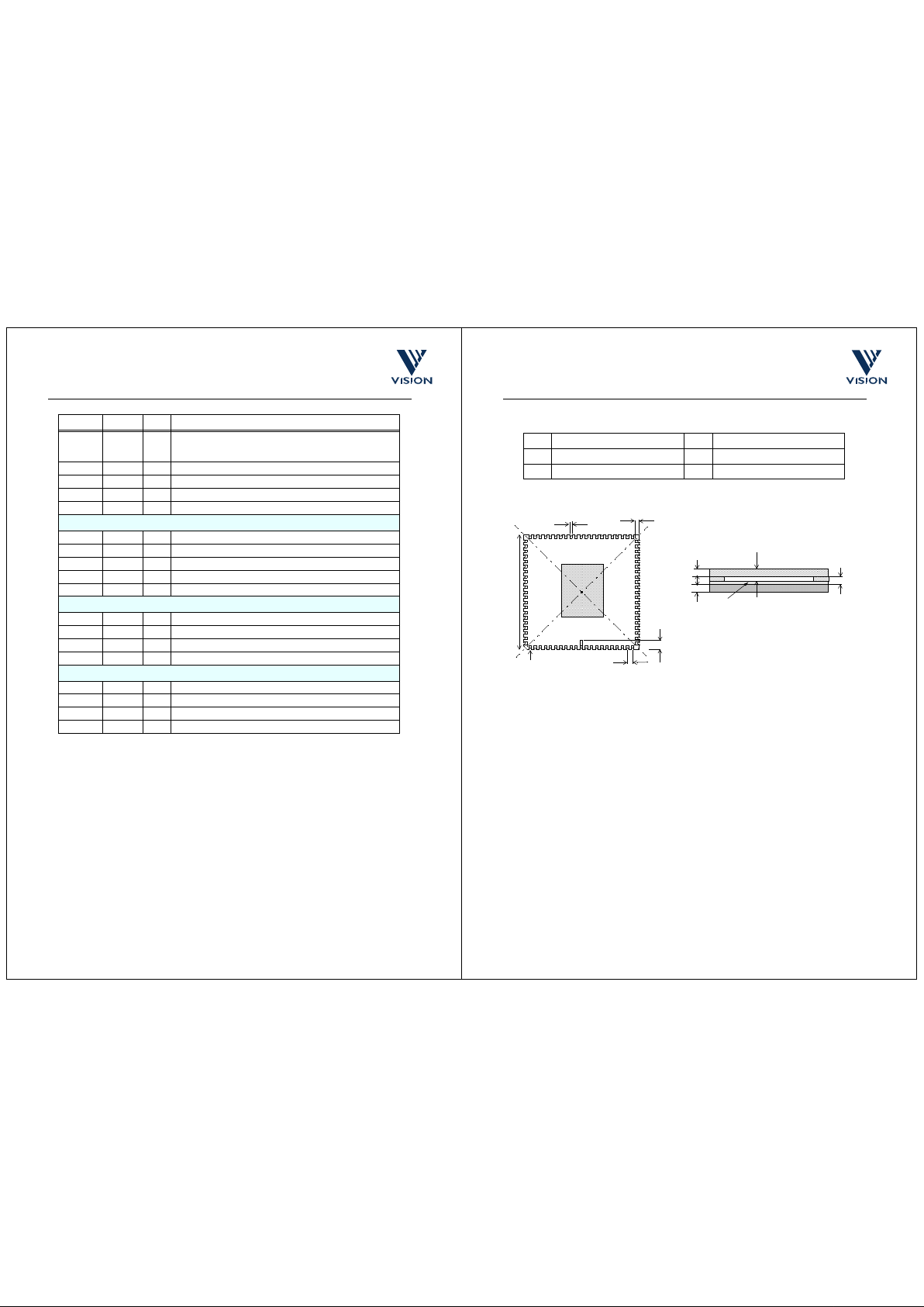
cd24082b.fm 09/09/98: PRELIMINARY 41
VISION VV6801/5801 PRELIMINARY CUSTOMER DATASHEET Rev 1.1
Pr
e
l
i
mi
na
ry
73 CDSR ID↓Correlated Double Sampling: Control input to allow the row of pix-
els currently being read to be reset without advancing the reset
VSR.
67 VCLRB ID↑Clear Reset and Read VSR’s.
68 VSETB ID↑Preset the Reset VSR to all ones. The Read VSR is not preset.
69 FI I D Field Integrate: Resets VSR. High duration sets exposure time.
70 FR ID Field Read: Reads VSR. Starts field read out.
HORIZONTAL SHIFT REGISTER (HSR)
60 PCK ID Pixel clock
66 HCLRB ID↑Clear Horizontal Shift Register
59 LS ID Line Start: Starts horizontal scan/pixel output.
58 EC ID ODD/EVEN Column Sel ec t .
57 COLsam ID Sample the Column Source Follower Inputs (pixel row).
SERIAL DATA INTERFACE (SDI)
63 DIN ID↓Serial Data Input
64 DOUT OD S erial Data Output
62 DLAT ID↓Latch Serial Data into Control Register
61 DCK ID↓Serial Data Clock Must be generated by host.
5-BIT RESISTIVE LADDER DAC
22 Vdactop IA Voltage reference for the top of the resistive ladder
23 Vdac3/4 OA Three-Quarter-point of the resistive ladder (Unbuffered)
27 DNC Do not connect
26 Vdac OA DAC Output Voltage (Unbuffered)
Pin Name Type Function/Comment
cd24082b.fm 09/09/98: PRELIMINARY 42
VISION VV6801/5801 PRELIMINARY CUSTOMER DATASHEET Rev 1.1
Pr
e
l
i
mi
na
ry
Key:
9.2 Package dimensions
Figure 9.2 : 84 LCC Package details
OA Analogue output pad ID Digital input
IA A nal ogue input pad ID↑Digital input with internal pull-up
OD Digital output pad OD↓Digital output with internal pull-down
0.51 TYP
1.0 TYP
2.16
Pin 1
1.016 PITCH TYP
23.37
0.55
0.51
0.42
Glass Lid
Sensor
The optical array is centred within the
package to a toleran ce of +/ - 0. 2 mm
, and
rotated no more than +/ - 0. 5
o
Tolerances on package dimensions +/-0.2
All dimensions in mill im et res
Viewed from below
Optical Centre
Pin 11
Standard 84 Pin LC C
0.864 Min.
‘TOP’
Page 22
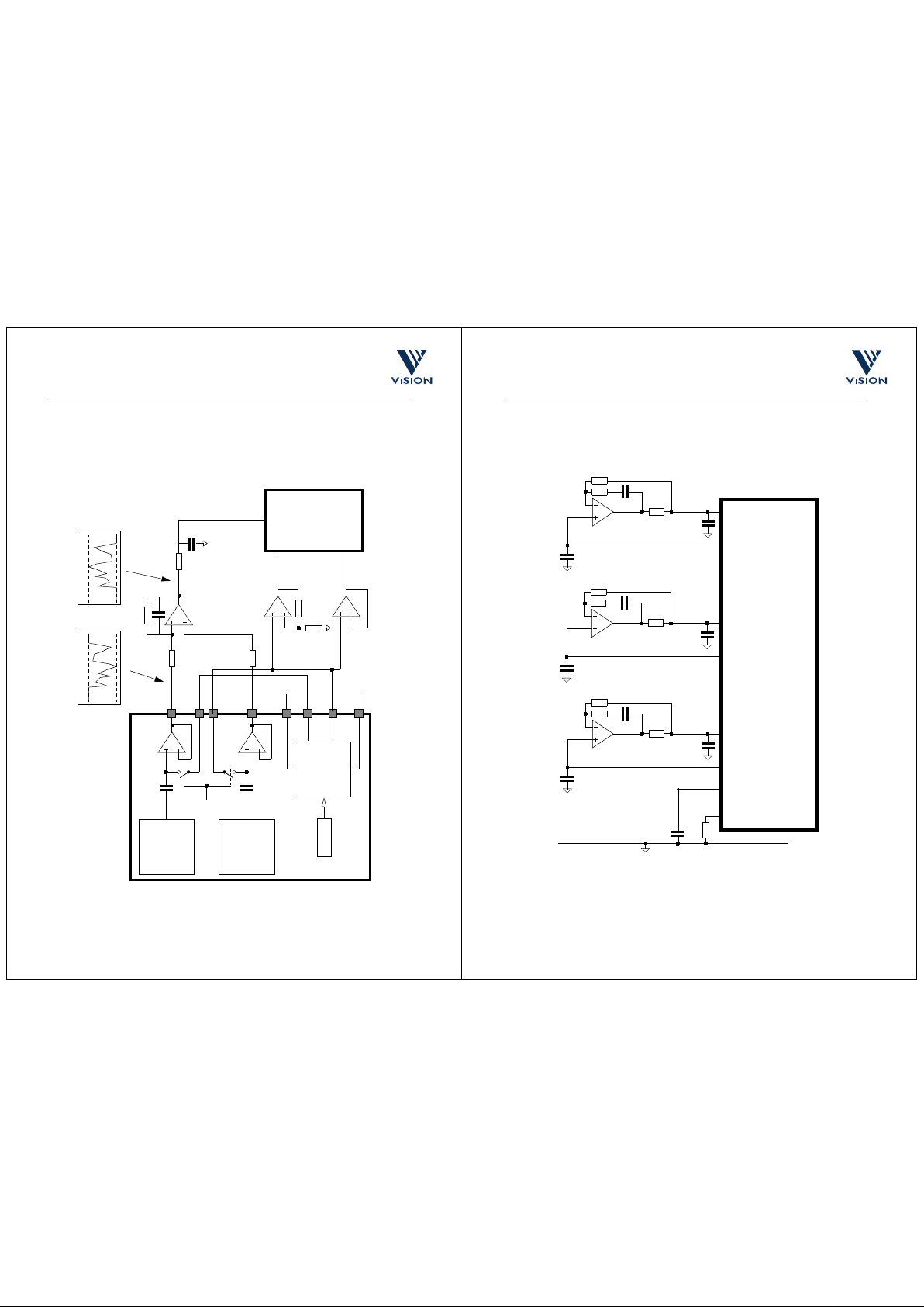
cd24082b.fm 09/09/98: PRELIMINARY 43
VISION VV6801/5801 PRELIMINARY CUSTOMER DATASHEET Rev 1.1
Pr
e
l
i
mi
na
ry
10. Support circuits and design guidelines
10.1 ADC Interface Circuit
AVO
AVORef
Sensor
Pipelined ADC
2k
Black
White
Black
White
REFTF
REFBF
Line
Reference
Pixel Array
+ Columns
VCL2
VCL1
CLAMP
5-bit
Resistor
Ladder DAC
Vdactop
Vdacbot
Vdac
Vdac3/4
25k
25k
2p
1k
1k
33
10p
A_IN
10 bit / 20 Msps
CR[15..11]
cd24082b.fm 09/09/98: PRELIMINARY 44
VISION VV6801/5801 PRELIMINARY CUSTOMER DATASHEET Rev 1.1
Pr
e
l
i
mi
na
ry
10.2 Analogue Reference Buffering
VV6801
VRT
VBloom
VBLTW
VBG
IC1-IC3 = Low Noise FET I/P OPAMPS
RSET
12K
VRTref
Vblmref
Vbltwref
1K
3K9
10
2n2
0µ1
0µ22
0µ11K3K9102n2
0µ1
0µ221K3K9102n2
0µ1
0µ22
IC1
IC3
IC2
Page 23
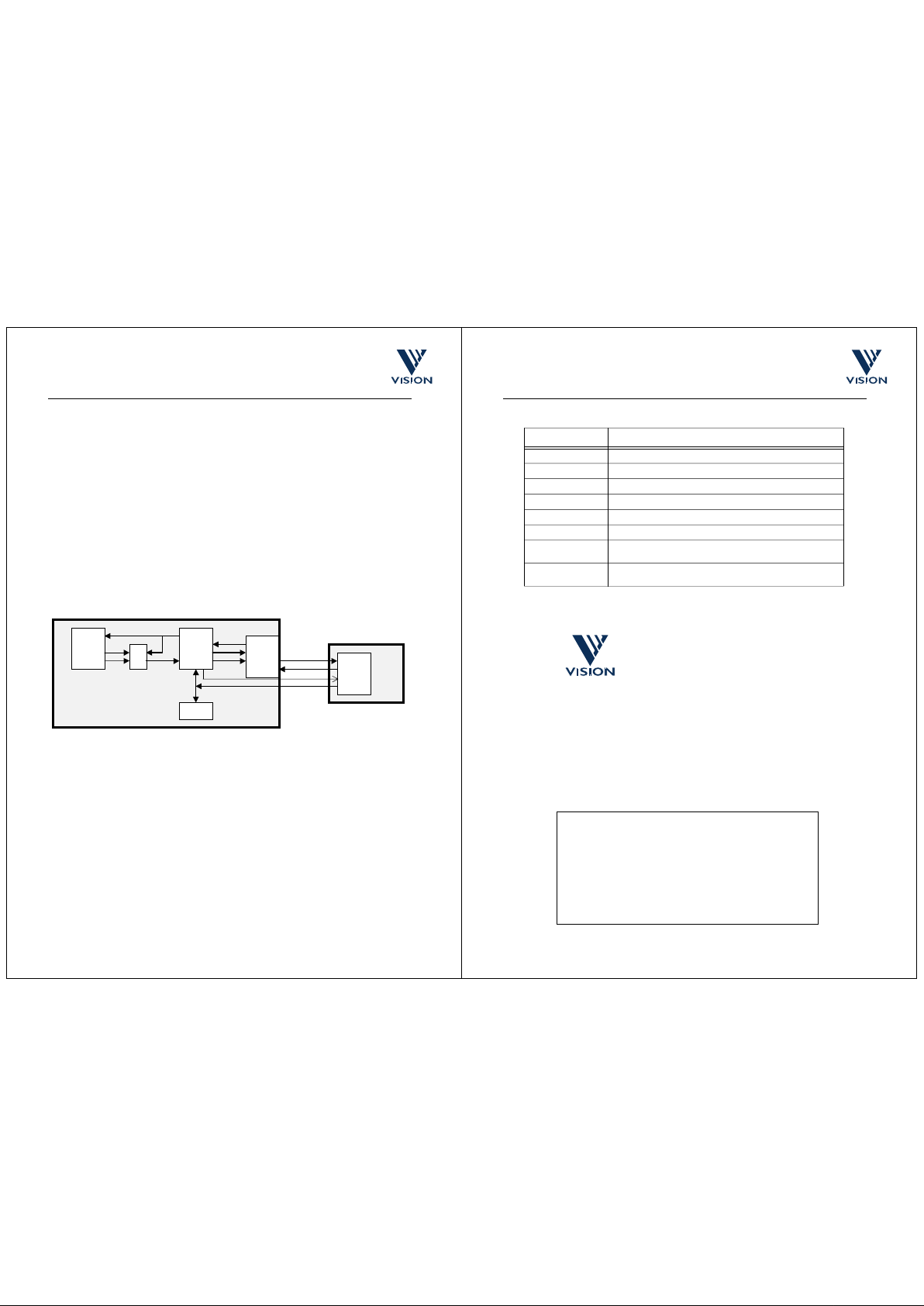
cd24082b.fm 09/09/98: PRELIMINARY 45
VISION VV6801/5801 PRELIMINARY CUSTOMER DATASHEET Rev 1.1
Pr
e
l
i
mi
na
ry
11. Evaluation kit (EVK)
It is highly recommended that an Evaluation Kit (EVK) is used for initial evaluation and design-in of the
VV6801 and 5801. For the VV5801 and VV6801 sensors, the EVK comprises a development board, including
a sensor, lens, and FPGA. It enables capture and display of images from the VV5801/VV6801 on a PC, using
the VISION software provided, in conjunction with a separate DT3157 Frame Grabber card (not supplied).
The Kit makes possible the evaluation of image processing and noise cancellation techniques as well as
providing a useful basis for development of VV5801/VV6801 custom hardware/software applications.
To assist existing VV5850 and VV6850 customers who may wish to evaluate and upgrade to the higher
resolution VV5801 or VV6801 devices an upgrade kit to the current VTD011 or VTD012 is available.
11.1 Key features
• VISION VV6850/5850 sensor with Lens mounting and C mount lens
• Digital interface to PC Framegrabber Card (not supplied) for fast image capture and storage
• Post Processing and sensor control software allows evaluation of sensor
• Exposure Control and Black Frame referencing
• Re-configuration of control FPGA possible and source code supplied for software
• Image storage in bitmap format possible
11.2 Block Diagram
HOST PC
DT3157
Frame
Grabber Card
RS 422
Drivers &
Receivers
Xilinx
XC4008E
FPGA
Data & Sync
Configuration
E
2
PROM
I/O
Sensor, Support
Circuit
ADC
Control
Data
Sync
AVO
Data
Sync
Control & Sync
VV6850/5850 Demon s trator
System
68 Way
RIBBON CABLE
AVORef
cd24082b.fm 09/09/98: PRELIMINARY 46
VISION VV6801/5801 PRELIMINARY CUSTOMER DATASHEET Rev 1.1
Pr
e
l
i
mi
na
ry
12. Ordering details
(*) Available shortly. Contact VLSI VISION for details.
Part number Description
VV6801C001
84LCC Colourised Sensor
VV5801C001
84LCC Monochrome Sensor
VV6801B001
BGA packaged Colourised sensor (*)
VV5801B001
BGA packaged Monochrome sensor (*)
VTD040
VV5801 (Monochrome) Digital Stills OEM Evaluati on Kit
VTD041
VV6801 (Colour) Digital Stills OEM Evaluat ion Kit
VTD044
VV5801 upgrade for VTD011 (VV5 850 (Mono) Digital Stills OEM
Development system)
VTD045
VV6801 upgrade for VTD012 (VV6850 (Colour) Digital Stills OEM Devel-
opment system)
Table 12.1 : Ordering details
VLSI VISION Ltd. reserves the right to make changes to its products and specifica-
tions at any time. Information furnished by VISION is believed to be accurate, but no
responsibility is assumed by VISION for the use of said information, nor any infringe-
ments of patents or of any other third party rights which may result from said use.
No license is granted by implication or otherwise under any patent or patent rights
of any VISION group company.
©
Copyright 1998, VLSI VISION
Distributor/Agent:
Aviation House, 31 Pinkhill,
Edinburgh EH12 7BF UK
Tel:+44 (0) 131 539 7111
Fax:+44 (0)131 539 7141
1190 Saratoga Ave. Suite 180,
San Jose CA 95129 USA
Tel: +1 408 556 1550
Fax: +1 408 556 1564
571 West Lake Avenue, Suite 12,
Bay Head NJ 08742 USA
Tel: +1 732 701 1101
Fax: +1 732 701 1102
VLSI VISION
LIMITED
www.vvl.co.uk
Email: [email protected]
 Loading...