

Page 1
VISION VV5430 Monolithic Sensor
Integrated CMOS Image Sensor with support
for ADC and external control via serial interface
PRODUCT DATASHEET
DISTINCTIVE CHARACTERISTICS
•• Complete Video Camera on a single chip
• EIA/CCIR standard compatible
• Low power operation (250mW Typical)
• Integral 75Ω driver
• Frame & line timing signals for external ADC
• Optional image output in four quarters, with output driver tristate option for multiplexing
GENERAL DESCRIPTION
The VV5430 is a high ly -integrated VLSI
camera dev ice based on VISION ’s unique
CMOS sensor technology. It is suitable for
applicat ions requir ing minimum ex t ernal
circuitry , digitisation of the video signal or
externa l m ic roprocess or control.
The dev ic e inc orporate s a 388 x 295 pixel
image se ns or and all the necessary s upport
circuits to g enerate composite video into a 75Ω
load. Additional control signals support pix el
locked digit is ation of the vi deo signal.
• Automatic Exposure and Gain Control
• Automatic Black Level Calibration
• Linear or Gamma corrected output option
• Control options pin selectable for ease of use
• External control/configuration via serial interface
• Industry standard 48 pin LCC package
y
A bi-direct ional serial in t erf ac e and inter nal
register set allow full con t rol and monitoring of
all camera fu nc t ions. Automatic control of
exposure , gain and blac k lev el give a wide
range of operating conditions. All major control
functions are pin selectable giving maximum
flexibility with ease of use.
The VV5430 offers a complete camera system
ideally suited for integration into digital imaging
systems.
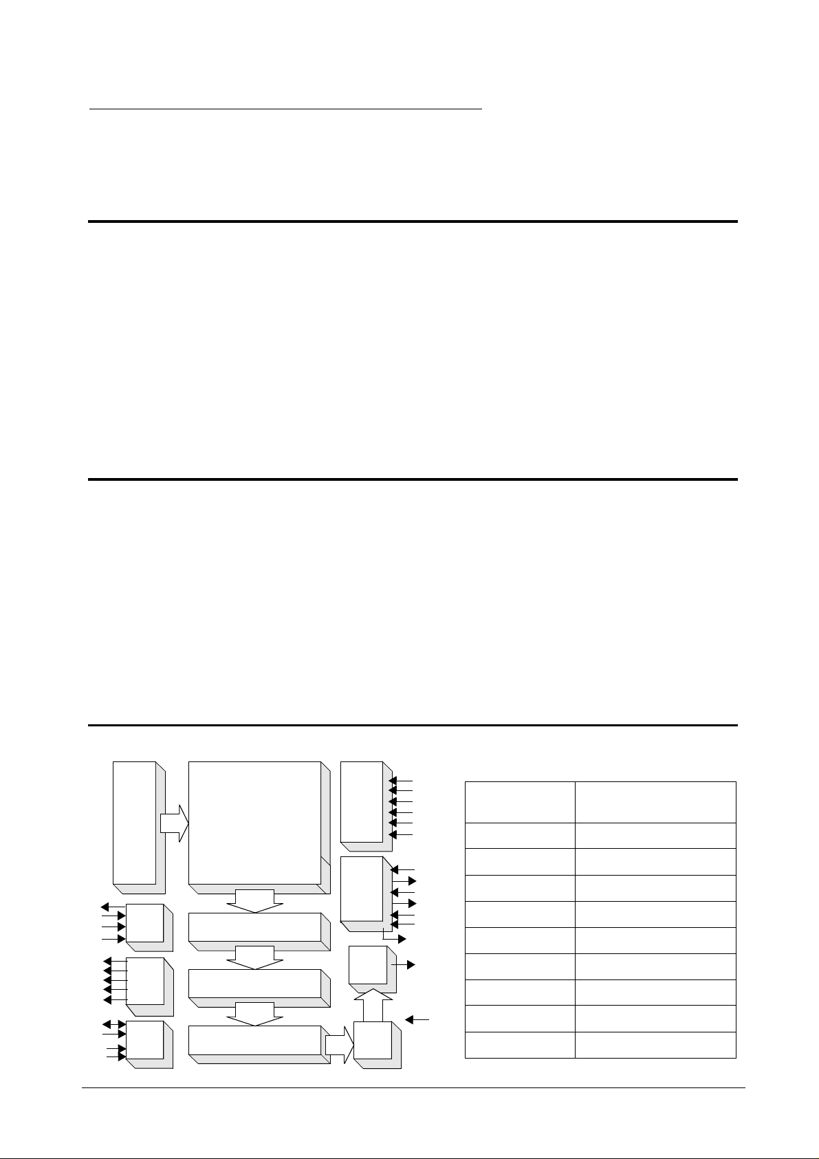
BLOCK DIAGRAM
AGC
VERTICAL
SHIFT
REGISTER
CKOUT
CKIN
SIN
CPE
FST
LST
PV
PVB
ODD
SDA
SCL
SAB0
SAB1
cd27033c.fm 1
CLOCK
CIRCUIT
IMAGE
CAPTURE
SERIAL
I/F
PHOTO DIODE ARRAY
COLUMN SENSE AMPLIFIERS
SAMP LE & H O LD
HORIZONTAL SHIFT REGISTER
Preliminar
DIGITAL
CONTROL
LOGIC.
ANALOG
VOLTAGE
REFS.
VIDEO
BUFFER
VIDEO
AMP
AEC
RESETB
LIN
BKLIT
CCIR
VRT
Vbloom
VOFF
VBG
EBCK
EVWT
2V7
AVO
Pixel Format 384 x 287 (CCIR)
320 x 243 (EIA)
Pixel Size 12µm x 12µm
Array Size 4.66mm x 3.54mm
Min. illumination 0.5 lux (Standard Clock)
S/N Typ ically 52dB
Exposure control Automatic (to 1460 00:1)
Gain Control Up to +20dB
Power Supply 5v ±5%
Power < 300 mW
5V
Temperature 0
o
C - 40oC
Page 2

VISION VV 5430 Sensor
MAIN FEATURES
The VV5430 deliver s a fu lly -f ormatted
composit e m onochro m e v ideo signal . S ta ndards optio ns inc lude EIA (3 20 x 244) and
CCIR (384 x 287). On chip signal conditioning
allows user-selecti on of linear or g am m acorrected output.
Different operationa l m odes can be s elected
dynamically via the e xternal inter fa c e or
configur ed at power up by tying the appropriate pins. Extensive use of automated operation and on chip references means that only
a small number of passive components are
needed to realise a com plete video camera.
Video Output
The integrated 75Ω driver eliminates the need
for additio nal active com ponents t o drive
standard loads, inclu ding double t erm inated
lines.
The video sig nal can also be inhibited by
setting the output to a high impedance state
(‘Tristate d’), which en ables multip lexing of a
number of different sensors. This, together
with vertical and horiz ontal ‘shuffle’ modes,
means that four sensor images can be shown
simultaneously on one display.
Frame, line and pixel timing signals are
provided t o f ac ilit ate pixel loc k ed digitisat ion
of the analo g v ideo data. In addition to th e
these outputs a synchronisation input (SIN) is
also provided to allow the start of frame to be
synchronised to an ex t ernal event.
elimina
Pr
Automatic Exposure and Gain Control
The VV5430 features autom at ic ex posure
control that allows a single fixed-aperture lens
to be use d, and incorpo rat es N ormal and
Backlit m odes to give operation over a wide
range of scene types. The system clock
frequency can also be reduced to provide
increased sensitivity.
Seri al Int e rf a ce
A bi-dire c tio nal serial interface allow s an
externa l c ontroller to s et operationa l parameters and co nt rol exposure and gain v alues
directly. T he host can al so int errogate
VV543 0 v ia t he serial interface to de te rm ine
the camera’s oper at ing modes and current
state. This allows alternative automatic exposure and other control algorithms to be run in
an external controller if the integrated
version s are not suitab le.
The VV5430 recei ve s and transm its c ontrol
and parametric data via a full duplex, two-wire
serial int erf ac e. The hos t is c om municat ions
master, with the camera either a slave
receiver or transmitter. Messages consist of
either three or five bytes of 8-bit data, with a
maximum serial clock frequency of 100kHz.
Since th e s erial clock is generated by th e
host, the host determines the data transfer
rate.
y
r
Contents
page
Main Features 2
Specifications 3
Pin List 7
Video Standards 9
Image Digitisation 12
Shuffle Modes 14
Exposure Control 17
Serial Com m unication 19
Read Data from Camera 21
Write to Camera 22
Example Support Circ uit 31
2 09/04/97
Page 3
SPECIFICATIONS
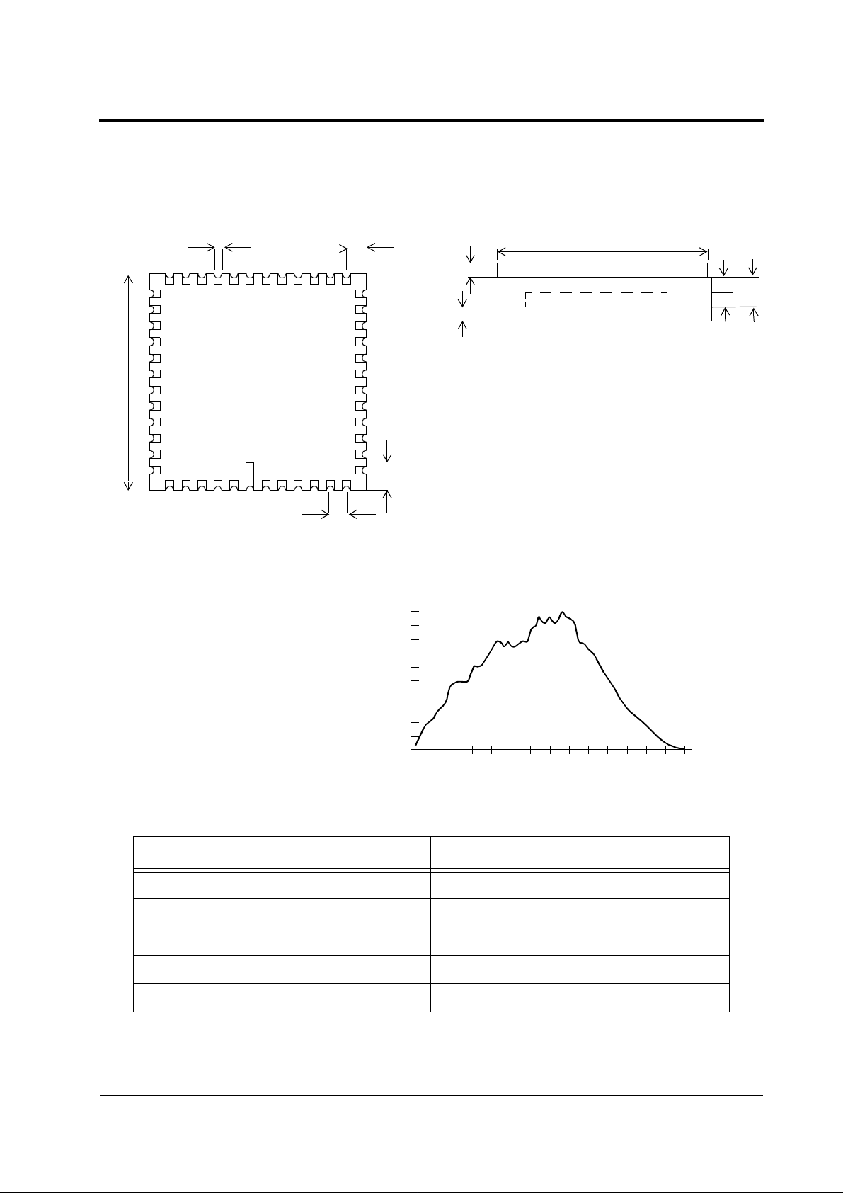
Package Details
Specifications
14.22
Viewed from below
Spectral Response
0.51
TYP
1.016 PITCH TYP
1.56 TYP
2.16
PIN 1
1.0
0.8
13.7
0.55
0.53
The optical array is ce nt red within th e
package to a tolerance of ± 0.2 mm, and
rotated n o m ore than ± 0.5
Toleranc es on package dimensions ±10%
Glass lid p lac ement is controlled so t hat no
packag e ov erhang ex is ts.
All dimens ions in millim et res
Glass Lid
Die
Base
Viewed from side
o
0.5
0.86
0.6
0.4
0.2
Normalised Response
0
400
500
600
700
800
900
1000
Preliminary
Wavel ength nm
1100
Absolute Maximum Ratings
Parameter Val ue
Supply Voltage -0.5 to +7.0 volts
Voltage on other input pins -0.5 to V
o
Temperature under bias -15
Storage Temperature -30
Maximum DC TTL output Current Magnitude 10mA (per o/p, one at a time, 1sec. duration)
Note: Stresses exceeding the Absolute Maximum Ratings may induce failure. Exposure to absolute
maximum ratings for extended periods may reduce reliability . Functionality at or above these
conditions is not implied.
C to 85oC
o
C to 125oC
+ 0.5 volts
DD
09/04/97 3
Page 4
VISION VV 5430 Sensor
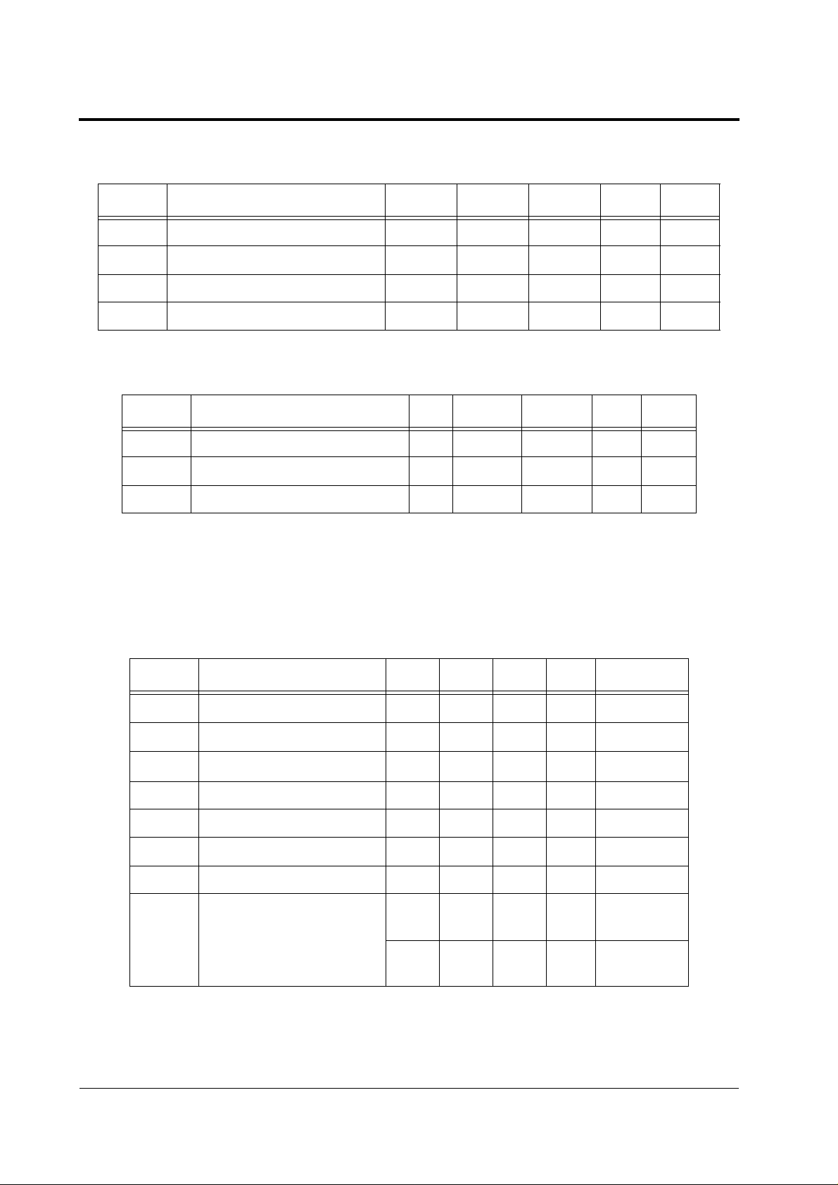
DC Operating Conditions
Symbol Parameter Min. Typ. Max. Uni ts Notes
V
DD
V
IH
V
IL
T
A
Operating supply voltage 4.75 5.0 5.25 Volts
Input Voltage Logic “1” 2.4 VDD+0.5 Volts
Input Voltage Logic “0” -0.5 0.8 Volts
Ambient Operating Temperature 0 70
AC Operating Conditions
Symb ol Par ameter Min. Typ. Max. Units No tes
CKIN
CKIN
SCL
1. Pixel Clock =
2. Serial Interface clock must be generated by host processor.
EIA Crystal frequency 12.0000 MHz 1
CCIR Crystal frequency 14.7456 MHz 1
Serial Data Clock 100 KHz 2
CKIN
/
2
Electrical Characteristics
y
o
C S t ill air
Symbol Parameter Min. Typ. Max. Units Notes
I
DCC
I
ADD
I
DD
V
REF2V7
V
BG
V
OH
V
OL
I
ILK
1. Digital and Analogue outputs unloaded - add output current.
Digital supply current
Analog su pply current
Overall s upply current
Internal voltage reference 2.700 Volts
Pr
Internal bandgap reference 1.22 Volts
Output Voltage Logic “1” 2.4 Volts I
Output Voltage Logic “0” 0.6 Volts I
Input Le ak age curren t
T ypical conditions, V
liminar
e
-1 µA
DD
10 mA 1
25 mA 1
35 mA 1
1 µA
= 5.0 V, TA = 27oC
= 2mA
OH
= -2mA
OL
VIH on
input
VIL on
input
4 cd27033c.fm
Page 5

Specifications
Operating Characterist ics
Parameter min. typ. max. units Note
Dark Current Signal 50 mV/Sec Modal pixel voltage due to photodiode leak-
age under zero illumination with Gain=1
= (Vt1 - Vt2)/(t1-t2), calculated over
(V
dark
two different frames
Sensitivity 6 V/Lux·Sec V
Min. Illumination 0.5 Lux Standard CCIR clock
Shading TBA % Variance of V
Random Noise -52 dB RMS variance of all pixels, at 66% satura-
Smear TBA % Ratio of V
Flicker TBA % Variation of V
Lag TBA % Average residual signal with no illumination
Blooming TBA Ratio of spot illumination level that produces
/Lux·10ms, where Lux gives 50% satu-
Ave
ration with Gain=1 and Exposure=10ms
over eight equal blocks at
66% satu r ati o n lev e l illuminati on
tion, over four frames
25 lines high illuminated at 500xV
to V
Ave
at 66% saturation level illumination
in the field following one field of 66% sat.
illumina tion
0.1xV
sat
spot to the V
hole target)
ave
of the area outside a rectangle
ave
of the rectangle
of one line from field to field
ave
output from immediately around the
spot illumination level (pin-
sat
50%
level
Note: Devices are normaly not 100% tested for the above characterisation parameters, other than
Dark Current Signal (see Blemish Specification below).
Preliminary
All voltage (VA, V
blemish es are excluded (see Blemish Specific at ion below ). V
of saturation, that is peak white.
T est Conditions
The sensor is tested us ing the exam ple support
circuit illus t rat ed later in this document . Sta ndard
imaging conditions used for optical tests employ a
tungsten halogen lamp to unif orm ly illuminate t he
sensor (to better tha n 0. 5%), or to illum inate
specific areas. A neut ral density filt er is us ed to
control the level of illum ination where require d.
09/04/97 5
ave
, V
sat
, V
) measurements are referenced to the black level, V
xx%
Illumination Colour T emp. 3200o K
Clock Frequency Std. CCIR
Exposure Maximum
Gain x1
Auto. Gain Control (AGC) Off
Correction mode Linear
refers to the output that is xx%
xx%
, and sp ot
black
Page 6
VISION VV 5430 Sensor
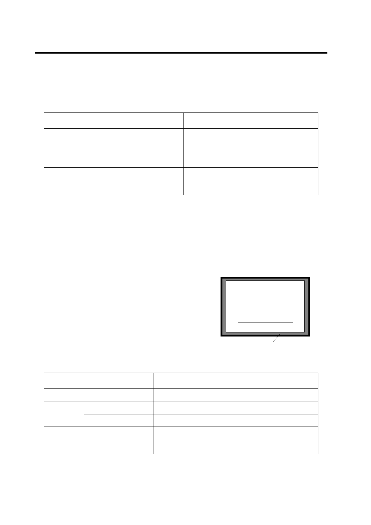
Blemish Specification
A Blemish is an area of pixels t hat produces output sig nif ic antly differe nt fro m it s su rrounding
pixels for the same illumination level. The definition of a Blemish Pixel varies according to testing
conditio ns as fo llows:
Test Exposure Illumination Blemish Pixel output definition
1 - Black Frame Minimum Black Differing more than ± 100 mV. from modal
value.
2 - Dark Current Maximum B lack Output more than three times the modal value
(see Dark Current Signal above).
3 - Pixel Variation Mid range 66% Sat. Differing more than ±35mV from modal value.
Note: The mode of pixel values must be within
±70 mV of 66% of V
for all devices.
sat
Note: Gain is set to Minimum and Correction set to Linear for all tests; measurement of blemishes for
Test 3 is conducted under standard illumination (see above), set to produce average output of
66% saturation level.
The pixel area of the sensor is divided into the following areas to qualify the blemish specification:
Area A is the central area of the array as defined
by the bo x wi th si des 50% of the linear height
and 50% of th e linear width of the array .
Area C is 10 vertical pixels by 10 horizontal pixels
aroun d th e edge of the array.
Area B is the remaining area of the array .
liminar
e
y
Area A
Area B
Area C
Pr
The blem is h s pecification is then def ined as follows :
Image Area Max. No. of Blemishes Notes
Area A 0 This is the most critical image area
4 Unconnected single pixels
Area B
Area C Any num ber Blemishes in this area are not significant, but the device
6 cd27033c.fm
1 Of up to four connected pixels (2x2 max.)
shall, however, have no row or column (>50% of row or
column) faults in any area.
Page 7
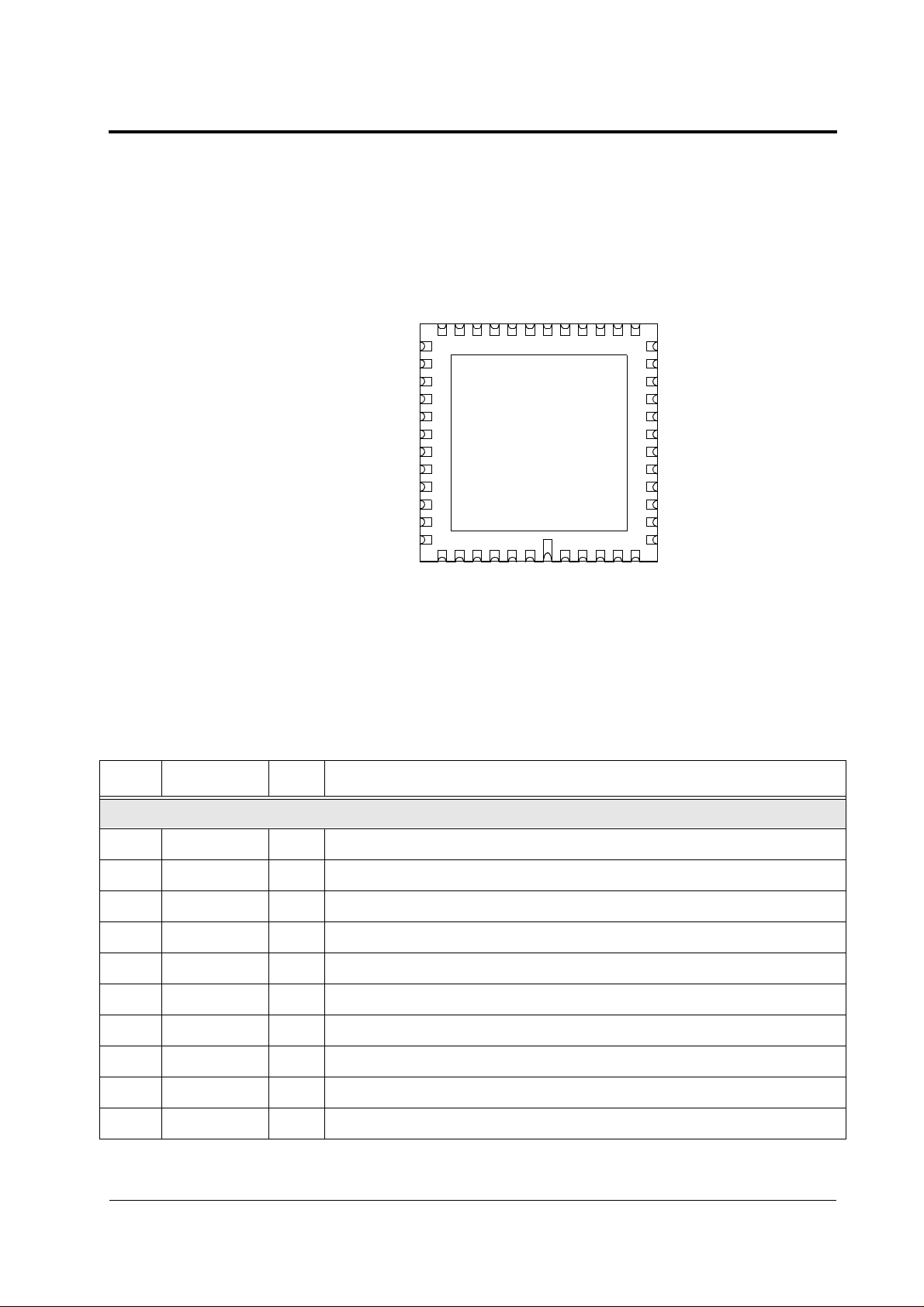
Pinout Diagram
48 Pin LCC
Viewed from top of package
VSS
PV
PVB
VDD
CPE
FST
ODD
SCI
SCL
SDA
VDD
VSS
31
32
33
34
35
36
37
38
39
40
Pin List
CKOUT
CKIN
VDD
BKLIT
RESETB
LST
41
42
VSS
AGC
CCIR
24 23 22 21 20 1930 29 28 27 26 25
LIN
AEC
SAB0
18
SCE
17
SIN
SAB1
16
15
VGND
14
AVO
13
VVDD
12
AMP2
11
AMP1
10
AVSS
9
EVWT
8
EBCK
7
AVDD
12345643 44 45 46 47 48
VRT
VBLWT
VCM
VBLOOM
VREF2V7
VBG
VPED
AVCC
AGND
VOFF/
DNC
DEC2V2
DEC2V7
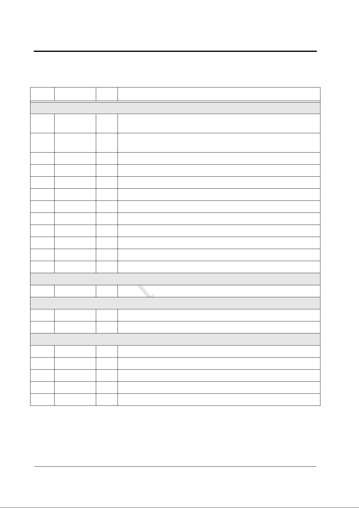
PIN LIST
Pin Name Type Description
POWER SUPPLIES
1 AVCC PWR Core analogue power and reference supplies.
7 AV DD PWR output stage power. AVDD3 output stage logic.
10 AVSS GND Output stage ground. AVSS3 output stage logic.
13 VVDD PWR 75ohm buffer supply .
15 VGND GND 75ohm buffer ground.
24,31 VSS GND Digital padring & logic ground.
Preliminary
27,34 VDD PWR Digital padring & logic power.
41 DVDD PWR Core digital power.
42 DVSS GND Core digital ground.
48 AGND GND Core analogue ground and reference supplies.
09/04/97 7
Page 8
VISION VV 5430 Sensor
Pin Name Type Description
ANALOGUE VOLTAGE REFERENCES
2 VBG OA Internal bandgap reference voltage (1.22V nominal). Requires external
0.1uF capacitor.
3 VOFF/VPED IA Pedestal DAC & offset comp. DAC bias. Connect to VBG or external ref-
erence.
4 DEC2V2 OA Decouple 2.2V reference. Requires external 0.1uF capacitor.
5 DEC2V7 OA Decouple 2.7V reference. Requires external 0.1uF capacitor.
6 - DNC Do NOT connect - for test use only
8 EBCK IA External black level bias. Internally generated. Decouple to VGND
9 EVWT IA E xte rnal white pixel threshold for exposure control. Decouple to VGND
43 VBLWT IA De fines white level for clamp circuitry. Requires external 0.1uF capacitor.
y
44 VBLOOM OA Anti-blooming voltage reference. Requires external 0.1uF capacitor.
45 VRT IA Pixel reset voltage. Connect to VREF2V7 or external reference.
46 VCM IA O ffset DAC common mode input. Connect to VREF2V7.
47 VREF2V7 OA Internally generated 2.7V reference. Requires external 4.7uF capacitor.
ANALOGUE OUTPUTS
14 AVO OA Buffered Analogue video out. Can drive a doubly terminated 75ohm load.
SYSTEM CLOCKS
25 CKOUT OD Oscillator output. Connect Crystal for standard timing.
26 CKIN ID Oscillator input. Connect Crystal for standard timing.
IMAGE CAPTURE TIMING SIGNALS
30 LST OD Line start. Active high pulse (start of active video lines).
32 PV OD Pixel sample clock. Qua lifies video output for external image capture.
33 PVB OD Pixel sample clock bar. Inverse of PV.
35 CPE ID↓ P ixel sample clock enable. Default CPE = 0 i.e. PV/PVB disabled.
36 FST OD Field start. Synchronises external image capture.
Pr
liminar
e
8 cd27033c.fm
Page 9

Pin List
Pin Name Type Description
37 ODD OD Odd/even field signal. (ODD = 1 for odd fields, ODD = 0 for even)
DIGITAL CONTROL SIGNALS
16 SAB1 ID↓ Higher bit of two least significant bits of device address on serial interface.
17 SIN ID↓ Used to reset video timing control logic without resetting any other part of
VV5430. Resets video logic on the falling edge of the SIN pulse.
18 SCE ID↓ Scan mode enable - only relevant to test mode.
19 LIN ID↓ Gamma corrected or Linear output. LIN = 0, gamma corrected output,
LIN = 1, linear output. Default is gamma. LIN = 0 can be overridden via
serial interface.
20 SAB0 ID↓ Lower bit of two least significant bits of device address on serial interface.
21 AEC ID↑ Automatic exposure control. AEC = 1, auto exposure is enabled; AEC = 0
auto exposure and auto gain control are disabled. AEC = 1 can be overrid-
den via serial interface.
22 AGC ID↑ Aut om atic gain control enable. AGC = 1, auto-gain is enabled (if AEC =
1); AGC = 0, auto-gain is disabled. AGC can be overridden via serial
interface.
23 CCIR ID↑ Select default video mode for power-on. CCIR = 1 for CCIR video. EIA
video mode is selected when CCIR = 0. Default is CCIR if unconnected
28 BKLIT ID↓ No rmal or Backlit exposure contro l mode. BKLIT = 0, normal mode.
BKLIT = 1, backlit mode. Default is normal. BKLIT state can be overrid-
den via serial interface. See Exposure Control for details.
29 RESETB ID↑ Active low camera reset. All camera systems are reset to power-on state.
38 SCI ID↓ Scan chain input - only relevant to test mode.
39 SCL ID↑ Serial bus clock (input only). Must be generated by comms. host.
40 SDA BI↑ Serial bus data (bidirectional, open drain).
Key:
Preliminary
OA - Analogue output IA - Analogue input
OD - Digital output ID - Digital input
OD↓ - Digital out put with internal pull-down ID↑ - Digital input with internal pull-up
BI - Bidirectional
09/04/97 9
Page 10
VISION VV 5430 Sensor
VIDEO STANDA RDS
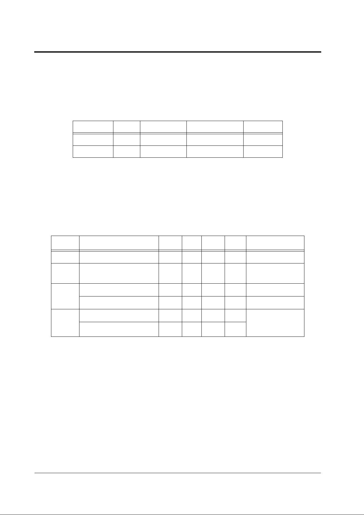
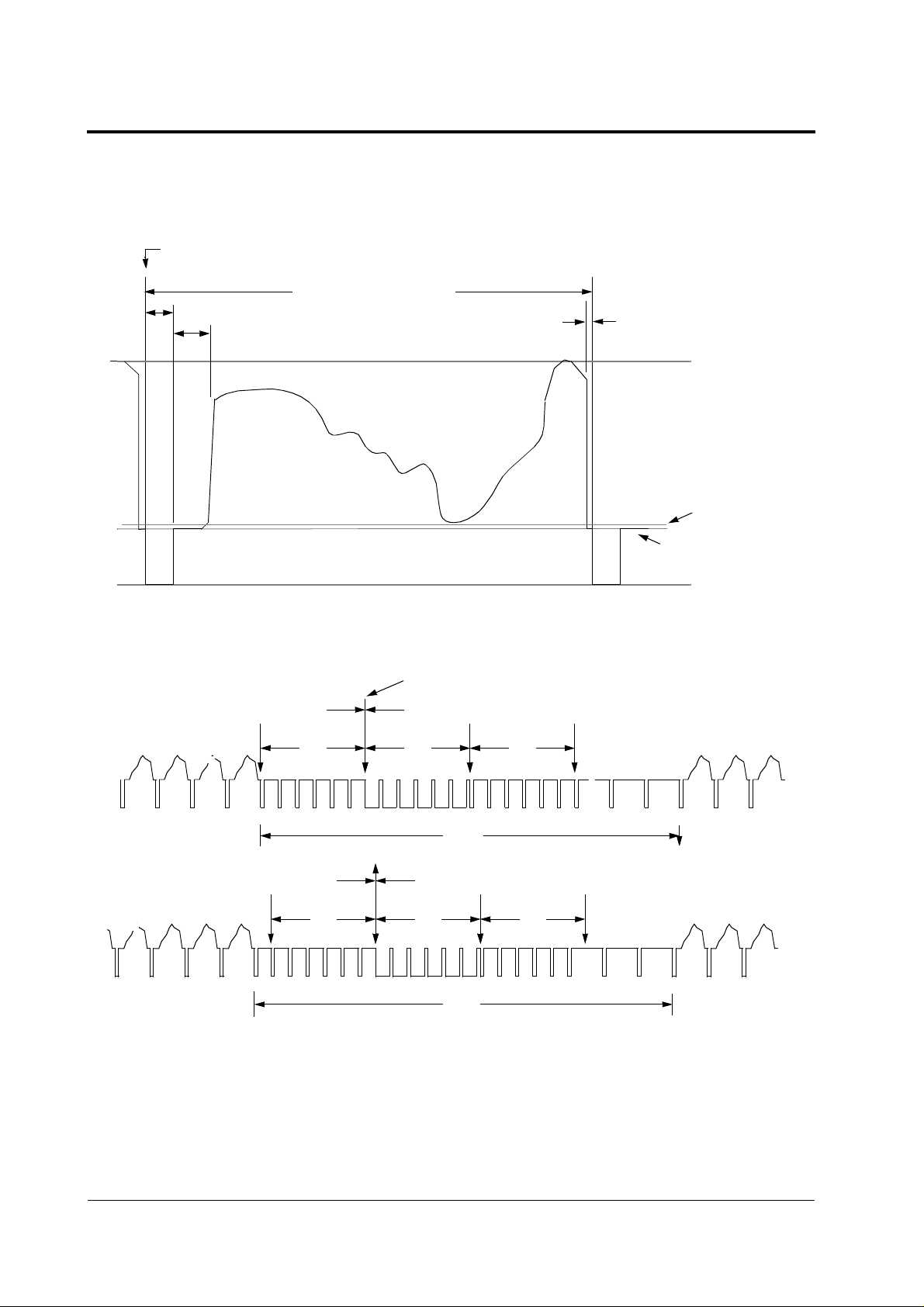
The VV5430 has 2 different video format modes, producing CCIR or EIA standard composite
Monoch rom e video ou tp ut . Line standards and frequ encies are as f ollows:
Video Mode Format Image (Pixels) Crystal Frequency CCIR pin
CCIR 4:3 384 x 287 14.7456 MHz 1
EIA 4:3 320 x 243 12.0000 MHz 0
VV5430 Video Modes
Video signal Characteristics
The following table summaris es th e c om posite video output lev els (AVO) for t he two standards,
which are graphically illustrated on the following pages:
y
Symbol Parameter Min. Typ. Max. Units Notes
V
V
V
V
Sync
blank
black
Sat
CCIR, EIA Sync. level
CCIR, EIA Blanking
level
CCIR Black level
EIA Blac k lev el
CCIR Saturation level
e
EIA Sat uration level
liminar
0.3 V
0.9 V
0.9 V
1.0 V
2.3 V
2.4 V
DC reference
level
Peak Whi te ;
AVO clipped at
this level
Pr
Note: All measurements are made with AVO driving one 75Ω load.
10 cd27033c.fm
Page 11
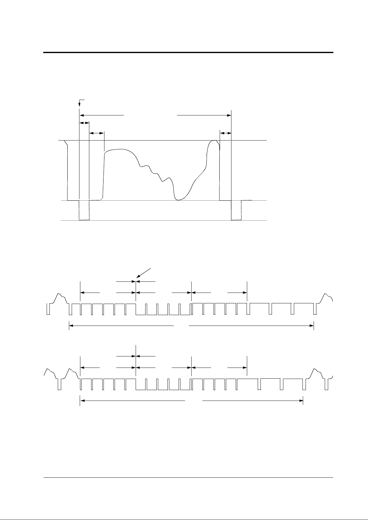
CCIR Timing Diagram
Video Standards
line time reference poin
line sync. 4.7µs
back porch 5.8µs
t
line period H = 64µs
front porch 1.5µs
peak white level
CCIR composite video signal - line level timing
frame start
rise times
(10% - 90%)
line blank 0.3 ± 0.1µs
{
line sync. 0.25 ± 0.05µs
2.3v
0.9v
0.3v
black &
blanking level
sync. level
field 0
2.5H 2.5H2.5H 2.5H
field 1
26H
Preliminary
field 1 field 2
2.5H 2.5H 2.5H
25H
CCIR composite video signal - field level timing
≈
≈
09/04/97 11
Page 12
VISION VV 5430 Sensor
EIA Timing Diagrams
line time reference point
line sync. 4.83µs
back porch 4.00 µs
rise times
(10% - 90%)
line period H = 63.5µs
front porch 1.33µs
peak white level
EIA composite video signal - line level timing
frame start
line blank 0.3 ± 0.1µs
{
line sync. 0.25 ± 0.05µs
2.4v
y
0.9v
0.3v
black level
1.0v
blanking level
sync. level
≈
≈
field 0 field 1
liminar
e
19H
field 1 field 2
Pr
20H
EIA composite video signal - field level timing
3H3H3H
≈
3H3H3H
≈
12 cd27033c.fm
Page 13
Control Signals for Image Digitisation
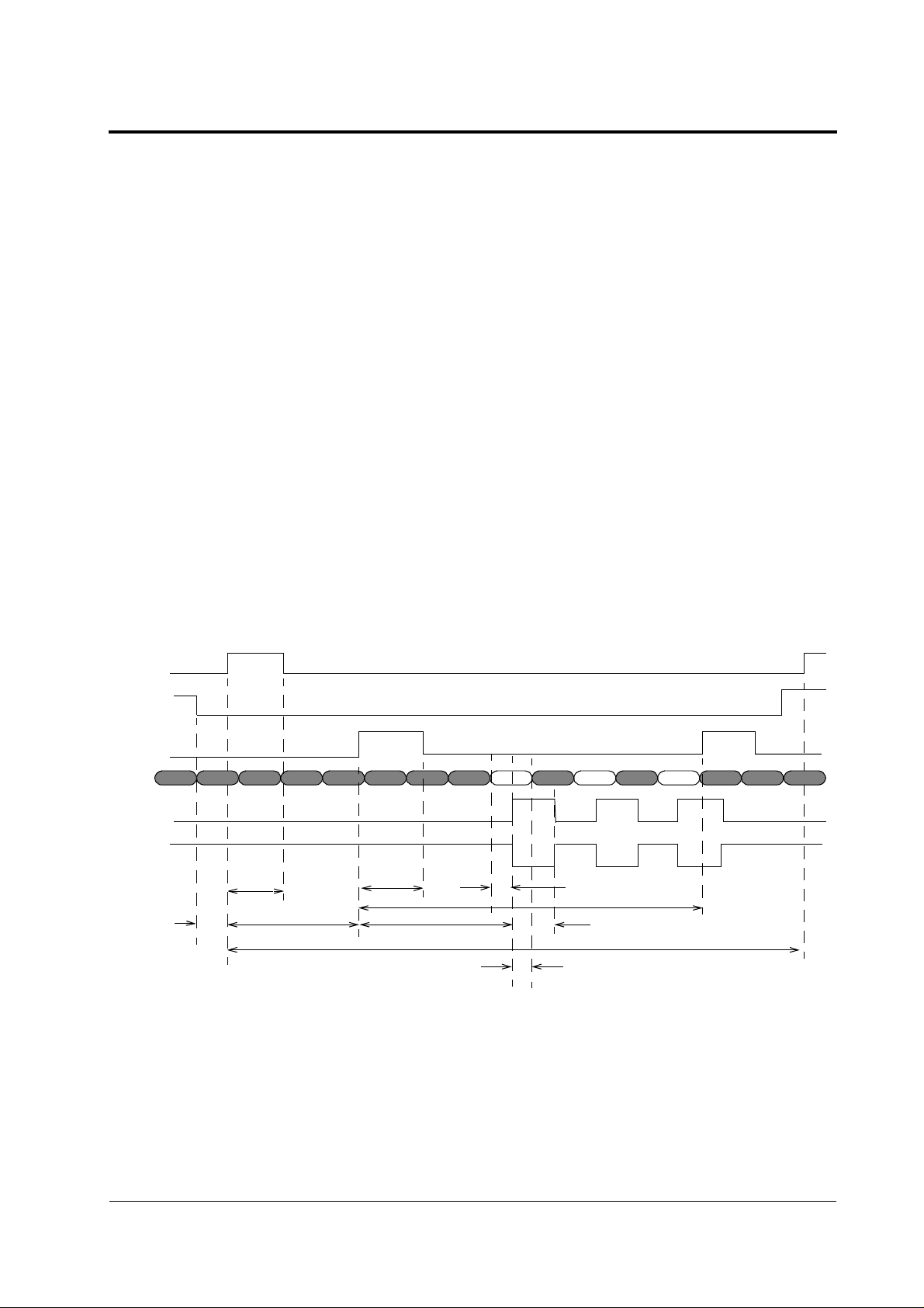
CONTROL SIGNALS FOR IMAGE DIGITISATION
The VV5430 camera can be used with an Ana log-to-Digit al Convert er (ADC) and t he necessa ry
logic to form an image capture and processing system. The camera provides an analogue video
output together with digital signals t o qualify this ou t put and synchronise image capture.
The signa ls provided for im age capture are the following:-
• PV,PVB: (Pixel Valid, PV Bar) Complementary signals, their leading edges qualify valid pixel levels.
• LST: (Line STart) The rising edge signals the start of a visible line.
• FST: (Field STart) The rising edge signals the start of a field.
• ODD: Identifies an odd field within a frame.
• CPE (Clock Pulse Enable): Disables generation of PV/PVB and LST signals. The state of this pin is
sampled only during a system reset. Its state after reset can be overridden via the serial interface
using Set-up Code_2.
The following diagram illustra te s th e relative timin g of th e im age capture signals. Sc ale is not
actual bu t e dge success ion is preserv ed.
FST
ODD
LST
AVO
PV
PVB
T
Todd
Preliminary
fst
T
blank
T
lst
T
porch
T
psu
T
phd
T
line
T
pv
T
field
Frame Capture signal timing
09/04/97 13
Page 14

VISION VV 5430 Sensor
Image Capture Control Signal Timing
The time int ervals give n are correct fo r th e recomme nded crystals :
Name CCIR EIA
Crystal Frequency (F
Pixel clock period (T
PV (Pixel clock) mark:space 1:1 1:1
PV high period (T
Even (first) field period (T
Odd (second) field period (T
FST duration (T
Line period (T
LST duration (T
First visible line delay (T
First visible pixel delay (T
Visible line period 52.083 µsec
pv
FST
) 64.0 usec
line
LST
) 14.7456 MHz 12.0000 MHz
CKIN
= 2/F
pck
= T
/2) 67.82 nsec 83.34 nsec
pck
field
) 7.73 µsec
) 4.61 µsec
blank
porch
e
) 135.63 nsec 166.67nsec
CKIN
) 20.032 msec
(313 x T
) 19.968 msec
field
(312 x T
line
line
)
)
y
(57 x T
(472 x T
(34 x T
) 704.949 µsec
(11xT
line
) 10.58 µsec
liminar
(78 x T
(384 x T
)
pck
)
pck
)
pck
+ 7xTpck)
)
pck
)
pck
(12xT
16.7005 msec
(263 x T
16.637 msec
(262 x T
6.1 µsec
(45 x T
63.5 µsec
(381 x T
4.66 µsec
(28 x T
762.833µsec
line
8.833 µsec
(53 x T
53.333 µsec
(320 x T
line
line
pck
pck
pck
+ T
pck
pck
)
)
)
)
)
pck
)
)
)
Max AVO to PV setup time (T
Min. PV to AVO hold time (T
ODD to FST rise (TODD) 21.700 msec
14 cd27033c.fm
Pr
) 33.9 nsec 41.7nsec
psu
) 30nsec 40nsec
phd
11.500 msec
(160 x Tpck)
(69 x Tpck)
Page 15
Shuffle Modes
SHUFFLE MODES
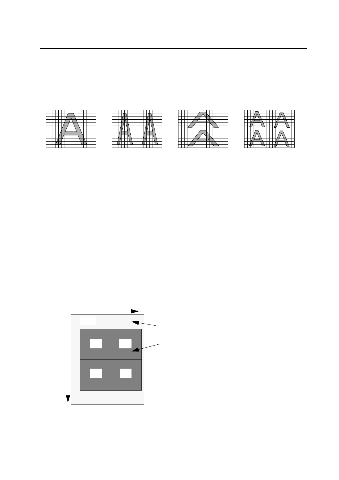
The pixel s in th e VV5430 se ns or array can be output to AVO as alternate colum ns and rows by
setting bit s 5 and 6 in the Se tu p C ode_1 regis t er (header c ode 0001 - see Serial Interf ac e for
details). This has the effect of generating two, or four, identical low resolution images in one field:
Unshuffled Image Horizontal Shuffle Vertical Shuffle Hor. + Vert. Shuffle
When this facility is combined with AVO Enable selected for the appropriate quarter, it is possible
to display t he images fr om f our separate cameras on one monitor.
In order to a c hieve four identical ima ges in one fram e (from one s ensor), bits 5 and 6 of Setu p
Code_1 must both be set via the serial i nt erfa ce, that i s HSHUFFLE=1 and VSHUFFLE=1. The
former interleaves odd and even pixel lines in the image, and the latter interleaves pixel columns.
OE[0..2] ca n t hen Enable AVO outp ut fo r any one quart er of t he display fie ld.
Quarter mode output
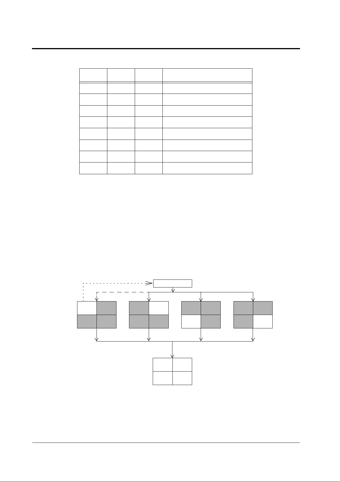
The VV5430 video output can be Enabled in different parts of the standard field by programming
bits 9..11 of Setup Code_2, that is CE[0..2]; when not enabled, the AVO output is Tristated, that
is floating at high impedance. Thus, a number of different sensor AVO outputs can be connected
together and selectively enabled. This feature, together with bus addressing of up to four VV5430s
on one serial link, is intended for multi-sensor systems that, in conjunction with bits 5,6 of Setup
Code_1, enable the images from up to four came ras t o be displayed on a singl e m onitor.
By program ming CE[ 0. . 2] dif f erent areas of th e f ield can be en abled:.
Pixels
Sync
Lines
Preliminary
Sync + Blanking
Q1 Q2
Q3 Q4
Image subdivided i nto 4 quarters :
CCIR: 384 pixels x 287 lines:
Q1,Q2 = 192 x 142
EIA: 320 pixels x 243 lines:
Q1,Q2 = 160 x 120
Q3, Q4 = 192 x 142
Q3, Q4 = 160 x 120
The effec t o f O E[ 0. . 2] on AVO outp ut is su m m arised in the f ollowing tab le:
09/04/97 15
Page 16
VISION VV 5430 Sensor
:
OE[2] OE[1] OE[0] Regions where AVO is enabled
0 0 0 All (Normal operation)
0 0 1 None (AVO permanently tristate)
0 1 0 Sync only
0 1 1 Sync plus Q1 image
100Q1
101Q2
110Q3
111Q4
AVO Enable selection
Since each of the horizontal ‘halves’ of the frame is only 142 lines (CCIR) or 120 lines (EIA), there
is a ‘black band’ of three lines separating the top half from the bottom ha lf . Sim ilarly, for tim ing
purposes, there is a two pixel vertical black band separating the left and right halves of the frame.
(See the timing diagram below. )
Multiplexing four cameras
Using the quarter mode of operation, it is possible, therefore, to combine the outputs of four separate VV5430 cameras (with app ropriate con trol logic) and display fo ur half resolut ion images on
one monit or:
Synchronisation
liminar
FST
Q1 Image + Sync.
SIN
A
A
Pr
AVO
A
A
e
SIN SIN SIN
B
B
AVO AVO
B
B
C
C
Composite Video
C
C
y
D
D
AVO
D
D
Monitor Display
A
C
Note: One VV5430 camera would normally be used as ‘master’, and provide the Sync-plus-Q1 out-
put for the monitor or other video device. A synch. signal, at frame frequency, is required via
SIN (pin 17) to keep the four cameras in step. This signal can be derived from the master camera FST output (with ‘SNO Enable’ set via Setup Code_3 bit 6), or be generated externally.
16 cd27033c.fm
B
D
Page 17
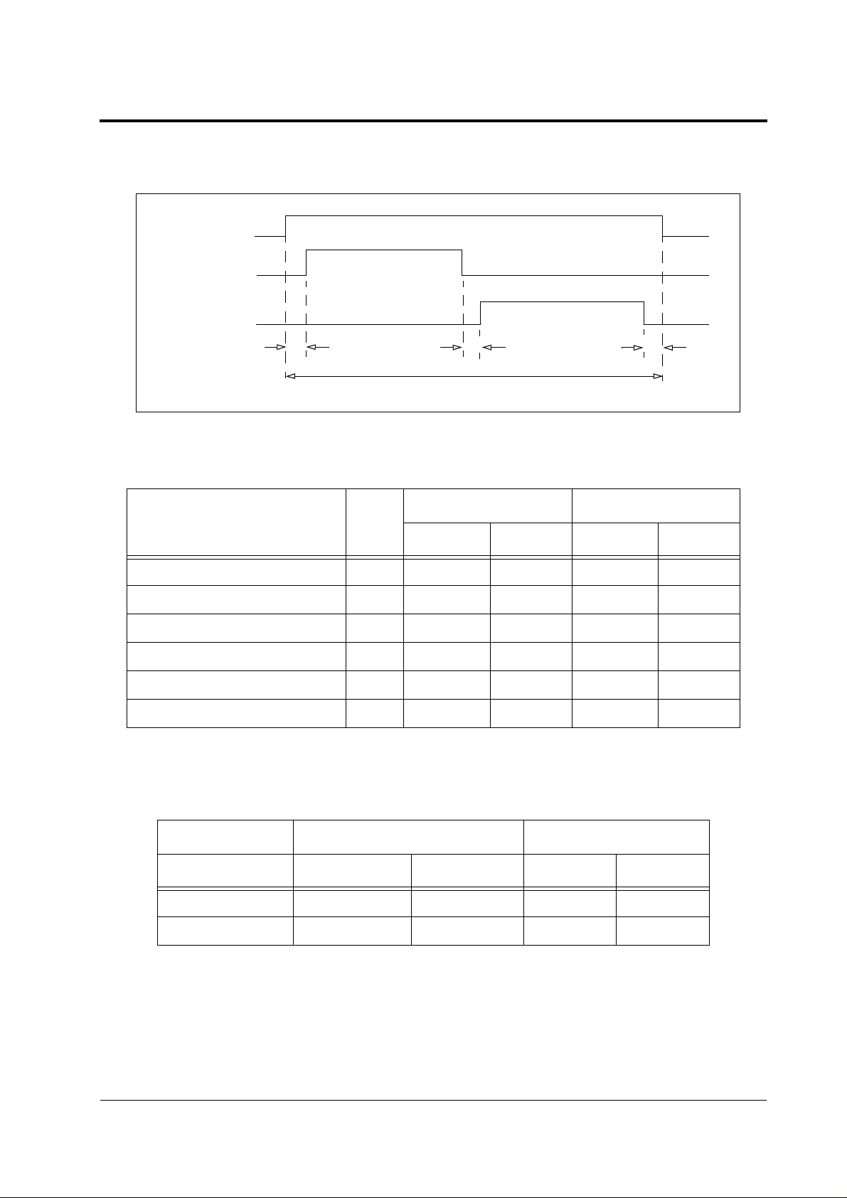
Quarter mode lin e timing.
Standard Line
Left Quarter
Right Quarter
Pixel timings for AVO 1/4 Mode:
Shuffle Modes
t1
t4
t2 t3
CCIR EIA
Description #t
pck cycles Time (us) pck cycles Time (us)
Left quarter Line Delay t1 1 0.1356 1 0.1667
Duration of left quarter line 190 25.4928 158 26.0052
Inter-quarter Interval t2 2 0.2713 2 0.3333
Duration of right quarter line 190 25.4928 158 26.0052
Right quarter border t3 1 0.1356 1 0.1667
Duration of standard SI t4 384 52.0704 320 53.3440
In additio n t here are line lev el signals to identify the to p and bottom half of the act iv e v ideo area
of the field: .
Description Start line Number of lines
Top half of field Fi rst active line First active line 142 120
Preliminary
CCIR EIA CCIR EIA
Bottom half of field Active line 145 Active line 124 142 120
There is a ‘b lac k band’ of three video line s bet w een the valid lines in the top half of th e f ield and
the valid lines in the bottom half of the field. This ensures that both halves of the field are the same
size and pr ov ides a horizontal fram e line. The line le v el t im ing described above als o provides a
two pixel v ert ic al black line, hence the fo ur quarters ap pear to be ‘fram ed’ in the display.
09/04/97 17
Page 18

VISION VV 5430 Sensor
EXPOSURE CONTROL
Automatic ex posure an d gain control ensure
oper at ion of th e VV 54 30 o ver a wi de ra nge of
lighting conditions. Automatic black level
control an d optional ‘B ac k lit ’ m ode further
ensure consistent picture quality. The
VV5430 controls exposure over a range of
99,000:1 in EIA mode and 146,000:1 in CCIR
mode, an d operates at illumination levels as
low as 0.5 lux.
Note: The System Clock can be divided by up
to eight times to further increase sensitivity by
extending the exposure time. Th is, of course,
also reduc es t he frame rate to non-standard
values.
Automatic ex posure an d gain control are
enab led with AE C=1 (pin 21 ) and AGC=1
(pin22), but c an be inhibit ed via the seri al
interface (Setup Code_1). However, If AEC is
inhibited by pin 21, AGC is also inhibited and
the serial in te rf ac e has no cont rol. Inhibit ing
AEC or AGC v ia t he serial interface, or by
taking pin 21 or 22 low, freezes the current
value(s) for these, whic h can then be altered
by writing to th e ex posure an d gain control
registers. (See Serial I nt erf ace for deta ils . )
Note: Th e t im ing of exposu re and gain con t rol
messages on the serial interface is very
importan t. Ex t ernal valu es fo r ex posure an d
gain are on ly applied at the s t art of a f ram e,
and the ser ial interface m us t be paused un t il
the new values are inst alled—no f urt her
communic ations will be ac c epted dur ing this
time.
elimina
Pr
Automatic Exposure Control (AEC)
Automatic ex posure control is ach iev ed by
varying pi xe l c urrent integration time
accordin g t o th e average light level on the
sensor. Th is int egration tim e can vary from
one pixel cl oc k period to one fr am e period.
is other than correct ly ex posed, a new v alue
for integ rat ion time is calc ulated an d applied
for the next f rame. Corrections a re either ±1/ 8
or ±1/64, depending upon the degree of over
or under ex posure. If the ex posure value is
close to it s limit (12% be low m ax. or 25%
above m in. ), t hen gain is increased or
decreased by one step and exposure is set to
midway in its range. Ex posure is the n
controlled as normal.
Automatic Gain Control (AGC)
The VV5430 automatically inc reases the
system gain of its output stage if with the
current gain setting and maximum exposure
the image is too dark. Gain can be varied from
x1 to x16 in times-two steps, giving five
differen t gain settings.
If the scene is too dark and the integration
period h as alm ost reach ed its maxim um
value, the gain valu e is inc remented by one
step (times two). In the same frame period the
exposure value is divided by two, halving the
integrat ion period. Th e ex posure controller
then incr eases the exposure value as necessary. Sim ilarly if the image is too bright and
the integration period is short then gain will be
reduced by one step (divide by two) and the
exposure value will be doubled. The exposure
controller can then adjust the exposure value
as necessary to provide a correctly exposed
image.
Increasing gain is limited to a programmable
upper limit, for which th e default va lue is x8.
The gain upper limit is programmed by setting
bits [0..3] with header code 0101, when
AGC=1. If Automatic Gain Control is inhibited
(AGC=0), these registers are used instead to
select a gain setting up to x16.
y
r
Pixels abo v e a t hreshold white level are
counted ev ery f ram e, and the number at th e
end of the frame defines the image as overexposed, ab ov e average , correctly exposed,
below average or underexposed. If the image
18 09/04/97
Page 19
Exposure Control
Backlit Mode
The VV 5430 can be co nfig ured to op erat e in t wo auto- expo sure mode s, s elec ted by the BKLI T pin
(pin28) st at e, or v ia the serial int erface (Set up Code_1, bit 0). T he default m ode (BKLIT = 0)
provides exposure control for normally illuminated scenes. For scenes where a bright background
can cause t he foregro und subject to be s ev erely under ex posed, th e ‘Backlit’ mode (BKLIT = 1)
offers sup erior perfor m ance.
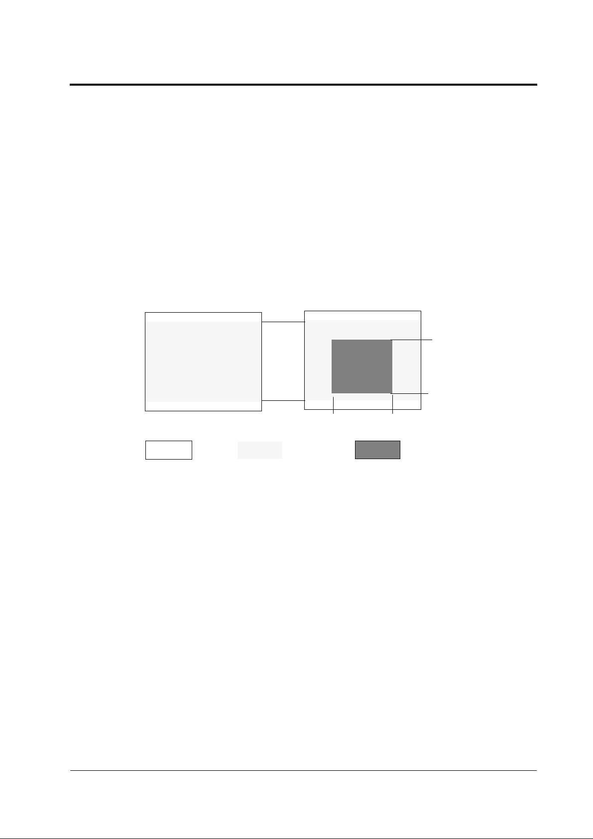
‘Backlit M ode’ (BKLIT= 1) operate s by us ing a higher th reshold level for the exp os ure control
compara t or over the ce nt ral area of an image, which is th erefore exposed for longer and s o
enhanced. The area in which the higher comparator threshold is used when BKLIT=1 is illustrated
below:
Normal operation (BKLIT=0) Hi gher threshold area (BKLIT=1)
10%
30%
80%
90%
25% 75%
Visible
image
Note: The threshold level used for the central area is a preset mutiple of the normal mode reference
level, and is not alterable.
Exposure
control area
25%
80%
Higher
Threshold
Preliminary
09/04/97 19
Page 20
VISION VV 5430 Sensor
SERIAL COMMUNICATION
The VV5430 includ es a f ull duplex (tw o-w ire) serial int erf ace, and ca n be controlled and con fi gured by a hos t processor . The base bus address fo r t he VV5430 is 20
cant bits of the address (SAB0, SAB1) can be selected by hard-wiring pins 20 and 16. This allows
up to four separate camera devices to be controlled on one serial link, which, for example, makes
multiplexing of cam era outputs pos s ible.
The seria l int erface reads or writes da ta to a se t of Re gis t ers that define the characterisatio n of
the sensor, and cont rol c ertain ope rat ions.
Serial Communication Protocol
The host must perform the role of a communications master and th e camera acts as either a slave
receiver or tr ansmitters co m m unication between host and ca m era takes the form of three or fi ve
byte messages of 8-bit dat a, w it h a m ax imum seria l c loc k (SC L) frequen c y of 10 0kHz. Since the
serial clock is generated by th e host, the hos t det ermines the data trans fe r rat e.
, but the two least signifi-
H
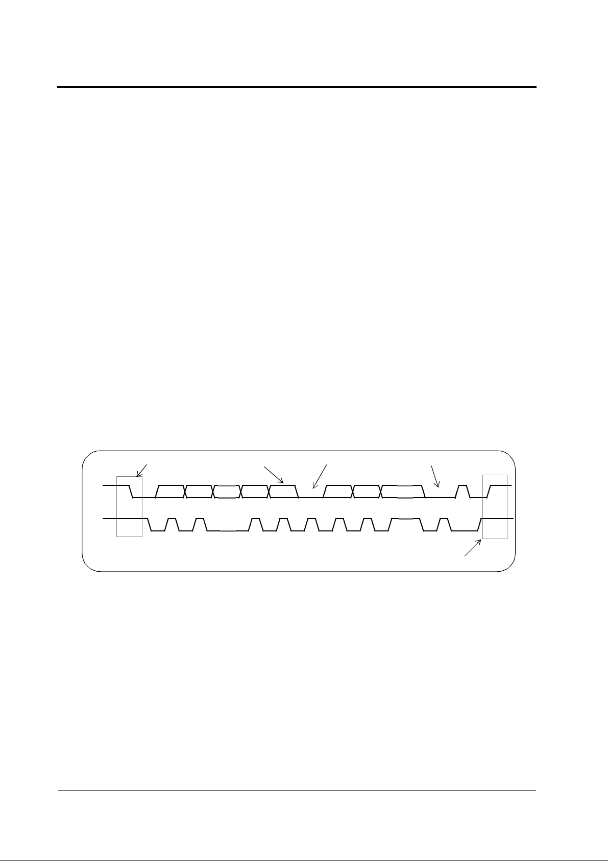
The host processor initiates a message by forcing both Serial Data (SDA) and Serial Clock (SCL)
low. The first byte addresses the required device, and defines either a READ message (four bytes
to follow) or a WRITE message (two bytes to fol low) . A fte r the ca mera has a cknowl edged a valid
address (ACK, bit 9 of SCL), the host then either reads four bytes of data from the camera or transmits a further two bytes to the camera. The data tran s f er protocol on the bus is illus t rat ed below:
Start condition
SDA
MSB
Read/Write bit Acknowledge from receiver
y
liminar
SCL
2
1
7891
e
ACK
2
3 - 8 9
ACK
Stop condition
PS
Pr
Data Transfer Protocol
20 cd27033c.fm
Page 21
Serial Communication
stopstartstop start
SDA
T
T
buf
T
lo
r
SCL
T
hd;sta
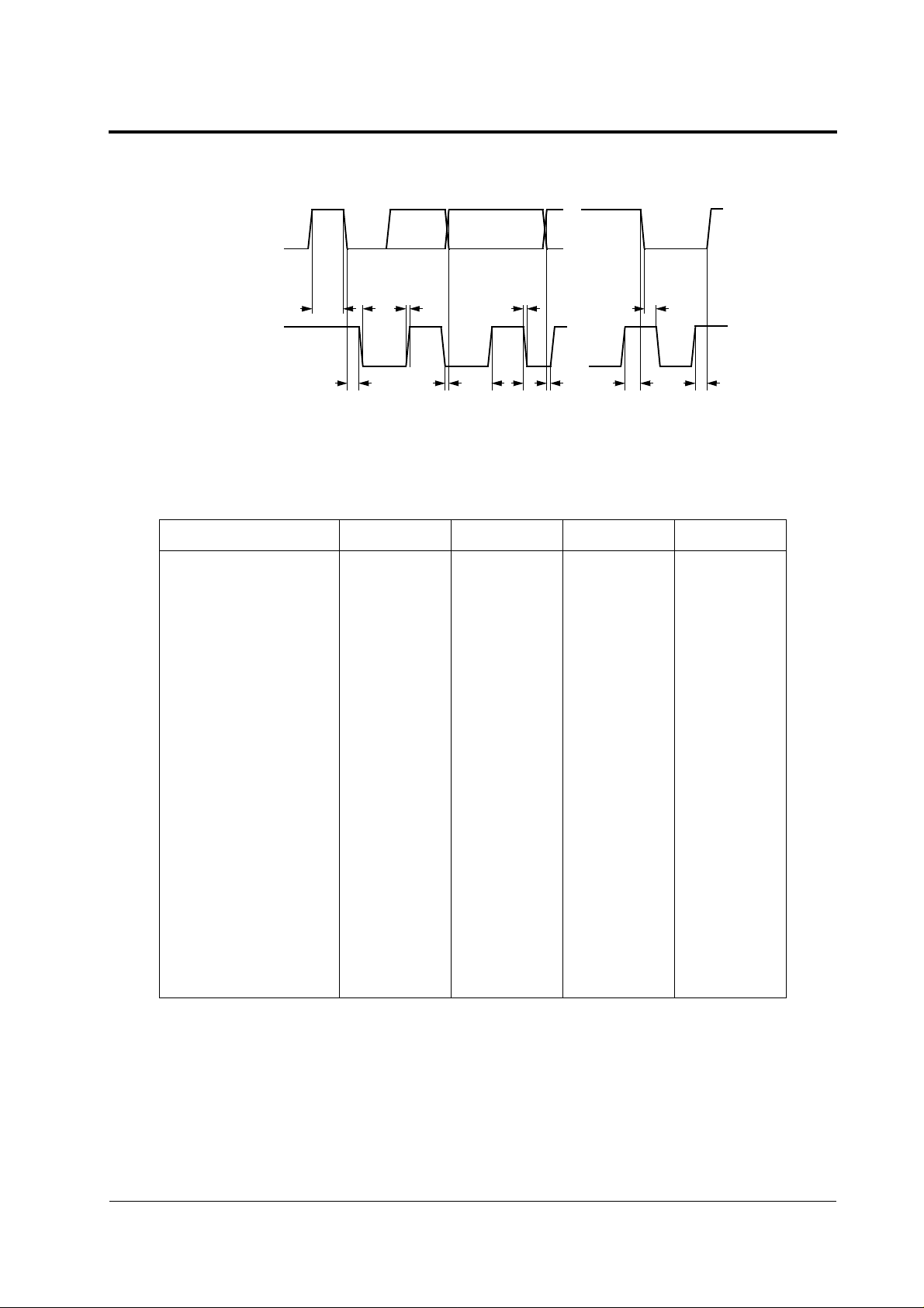
Note: All values referred to the minimum input level (high) = 3.5V, and maximum input level (low) = 1.5V
Parameter Symbol Min. Max. Unit
SCL clock frequency F
Bus free time between
a stop and a start
Hold time for a
repeated start
scl
T
buf
T
hd;sta
T
hd;dat
T
hi
0100kHz
4.7 - µs
4.0 - µs
...
T
f
T
hd;sta
...
T
su;dat
T
su;sta
T
su;sto
LOW period of SCL T
HIGH period of SCL T
Set-up time for a
repeated start
Data hold time T
Data Set-up time T
Rise time of SCL, SDA T
Fall time of SCL, SDA T
Set-up time for a stop T
Capacitive load of each
bus line (SCL, SDA)
1. The VV5430 internally provides a hold time of at least 300ns for the SDA signal
(referred to the minimum input level (high) of the SCL signal) to bridge the undefined region of the falling edge of SCL
Preliminary
lo
hi
T
su;sta
hd;dat
su;dat
r
f
su;sto
C
b
4.7 - µs
4.0 - µs
4.7 - µs
1
0
250 - ns
- 1000 ns
-300ns
4.0 - µs
-100pF
-µs
Serial Interface Timing Charac teri stics
09/04/97 21
Page 22
VISION VV 5430 Sensor
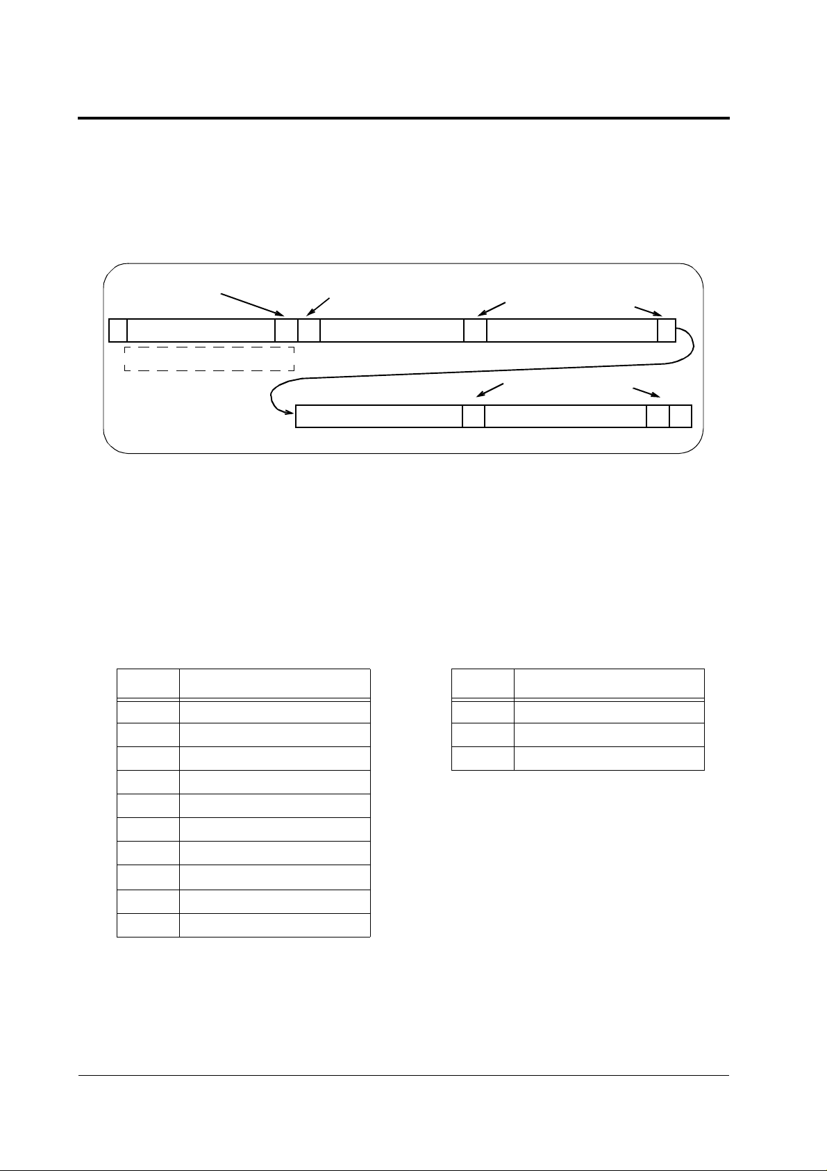
READ DATA FRO M CA ME R A
Information describing the current configuration and the current exposure values can be read from
the camera. The data is formed into four bytes of 8 bits. E ach pair of bytes is considered to be a
data word and is read out msb first.
Read = 1
S
ADDRESS[7:1] DATA[31:24]
0 0 1 0 0 x x 1
The following tables defines th e inf ormation contained in th e read messa ges. By default, the
Primary Read Data is a ccessed; only if a Secondary Read Select bit is set in Setup Code_2
(header co de 0010) is the Seconda ry inf ormation read.
Primary Read Data:
Bit Function
Camera acknowledge (valid address)
R
/
AA A
W
DATA[15:8] DATA[7:0]
Read Data Format
A
Secondary Read Data:
Master acknowledge
DATA[23:16]
Master acknowledge
AP
y
Bit Function
liminar
31 - 23 Coarse Exposure Value (9 bits)
22 - 14 Fine Exposure Value (9 bits)
e
31 - 18 Undefined
17 Blac k Level monitor in progress
13 - 10 Gain Value (4 bits)
9 Auto Exposure Control on/off
8 Internal Black Calibration on/off
7 Auto Gain Control on/off
6 Gamma or Linear Video Output
5
4 Undefined
3 - 0 Camera Type ID Code (4 bits)
1. Bit 5 of the Primary Read message only reflects the
22 cd27033c.fm
Normal or Back lit mode
state of the BKLIT pin, not the combined result of
the pin and the serial interface BKLIT control bit.
Pr
1
16 - 0 White Pixel count (17 bits)
Page 23
Write to Camera
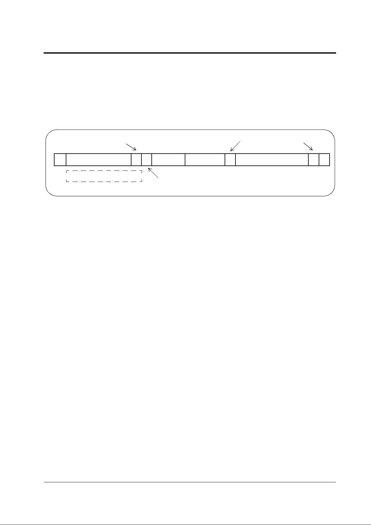
WRITE TO CAMERA
Information to be communic ated f rom host to camera consists of conf igura ti on d ata ( fo r exampl e
automatic gain control ON), and parametric information (for example sensor integration time). The
write data is formed into two bytes. A 4-bit Header Code in the first byte is used by the camera to
determin e t he destinat ion of the 12-bit message fo llow ing the he ader.
Write = 0
R
S
ADDRESS[7:1]
/
W
A
HEADER
DATA[11:8] DATA[7:0]
Camera acknowledge
AAP
0 0 1 0 0 x x 0
Camera acknowledge (valid address)
Receive Data Format
After the camera acknowledges the receipt of a valid address the host transfers the first data byte
which the camera acknowledges by pulling SDA low. The second byte is then sent followed by a
final acknowledge fro m th e c amera. A stop condition is produced by t he host after t he second
message byte. As with the read procedu re, th e stop condition is not abs olutely nec es s ary as the
camera’ s se rial interface w ill reset automatically after two bytes have been re c eiv ed.
The valid Header Codes and their data structures are fully described in the following pages.
Timing Protocol
When an exposure or gain value has been written to the camera it is held in the interface until the
camera is ready to consume the new data. For correct operation, there should be no further read
or write acc es s es to the cam era during th is hold period. N orm al commu nic ation between other
modules connected to the serial interface will not cause problems. The minimum length of the wait
period is
09/04/97 23
40ms in EIA mode and 34ms in CCIR mode from the end of the data transfer.
Preliminary
Page 24

VISION VV 5430 Sensor
Header Codes
The message can be a configuration word, an exposure, gain or calibration value. The camera’s
interpret at ion of the header code a nd t he set-up code messag e are given in the ta ble below.
Defaults fo r eac h control bit are built in to th e c am era’s reset c ycle, and may be changed on-thefly under h os t co nt rol.
Code Interpretation Comment
0000 Invalid
0001 Set-up code_1 (9 bits) Basic funtionality options
0010 Set-up code_2 (9 bits) Pixel control & Read Data
001 1 Coarse exposure value (9 bits) Set AEC=0 to enable
0100 Fine exposure value (9 bits) Set AEC=0 to enable
0101 Gain control value (4 bits) S et AG C=0 to enable
0110 Unused
0111 Unused
1000 Exposure control T1 threshold (9 bit)
1001 Exposure control T2 threshold (9 bit)
1010 Analogue control register (8 bit)
1011 Reserved Not applicable to normal use
1100 Reserved Not applicable to normal use
1101 Reserved Not applicable to normal use
1110 Set-up code_3 (6 bits) Pixel synchronisation
1111 Test mode select Not applicable to normal use
Message content
e
Pr
y
liminar
Header Codes
The following Table s co nt ain details of th e data associa t ed with each header code , and the
number of va lid data bits in eac h of the regis t ers . In all c ases the full 1 2 bit m es s age tail can be
sent, the valid bits being packed to the lsb. (Normally, the unused bits would be assigned zeroes.)
24 cd27033c.fm
Page 25

Write to Camera
Setup Code_1
Header Code = 0001 Valid data bits: 11
The code_1 setup register is used to select d ifferent basic operating modes:
Bit Function Default Comment
0 Normal/Backlit 0 Selects between normal and backlit exposure
modes. The power-on default is normal mode. See
Exposure Control for full description
1 Linear Correction enable 0 Selects betwee n a linear (LIN=1) or gamma cor-
rected video signal on AVO. The power-on default is
gamma corrected.
2 Auto gain control enable 1 Allows automatic gain control to be inhibited. The
current gain value selected is frozen. With AGC=0 a
new gain value can be written to the gain register via
the serial interface (header code 0101).
3 Inhibit black calibration 0 Allows automatic black calibratio n to be inhibited.
4 Auto exposure control enable 1 Allows automatic exposure control to be inhibited.
The current exposure value selected is frozen. Note
that if automatic exposure control is inhibited then
automatic gain control is also disabled. With AEC=0
a new exposure value can be selected by writing to
the coarse and fine exposure registers via the serial
interface (header codes 0011 & 0100).
5 Horizontal shuffle enable 0 Shuffles the read out of the horizontal shift register.
Even columns read out together then odd columns.
6 Vertical shuffle enable 0 Shuffles the readout of the vertical shift register.
Even lines read out together then odd lines.
7 Force black calibration 1 Requests a re-calibration of the black level while bit
is low.
8 Clock divisor DIV0 0 Sy stem clock division: (see Note)
9 Cl ock divisor DIV1 0
10 Internal Register 1 This bit must be set(=1) for correct sensor operation
11 Not used 0
Preliminary
0,0=1; 0,1=÷2; 1,0=÷4; 1,1=÷8
Set-up code_1
Note: Decreasing the system clock rate proportionately increases sensor sensitivity (by i ncreasing
exposure time), but also decreases frame frequency. System Clock must be x1 for standard
CCIR or EIA framing.
09/04/97 25
Page 26
VISION VV 5430 Sensor
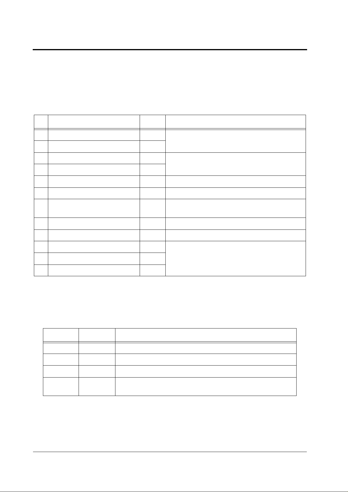
Setup Code_2
Header Code = 0010 Valid data bits: 12
The code _2 setup regis t er is used to select read dat a, valid pixels and video ou t put operating
modes:
Bit Function Default Comment
0 Shadow read mode (A) enable 0
1 Shadow read mode (B) enable 0
2 Pixel sample clock select (SEL0) CPE
3 Pixel sample clock select (SEL1) 0
4 Not used 0 MUST be set to 0
5 E nable free running pixel clock 0 Overrides SEL0 & SEL1.
6 Enable external pixel thresholds 0 Use external algorithm thresholds in exposure con-
7 Not used 0 MUST be set to 0
8 Not used 0 MUST be set to 0
9OE[0] 0
10 OE[1] 0
11 OE[2] 0
Select shadow read mode A or B.
Note: bits 0,1 are mutually exclusive.
Pixel sample clock mode (PV/PVB). See below.
troller
AV O output enable control bits [0..2]. See Shuffle
Modes above for explanation.
Setup Code_2
y
liminar
The table below shows the function of SEL0 and SEL1 (Bit 2 and Bit 3); the default value of SEL0
is set by the CPE pin level:
Bit 3 Bit 2 Pixe l Clock (PV/PVB pins) function
0 0 Disable pixel clock output
0 1 Qualify full image area (as defined for CCIR or EIA)
1 0 Qualify central 256 x 256 pixels (CCIR only)
1 1 PV/PVB active only during interline periods of visible image lines.
26 cd27033c.fm
Pr
e
Note. This mode is required for digitisation of standard video output.
Page 27
Write to Camera
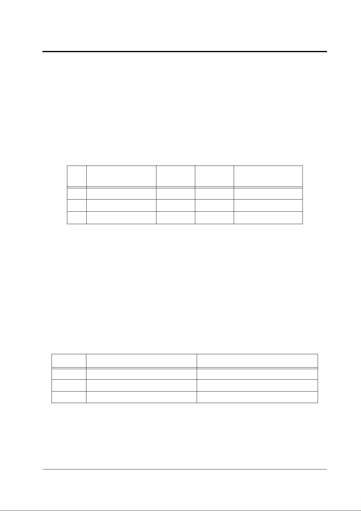
Coarse and Fine Exposure Values.
Header Code (coarse) = 001 1 Valid data bits: 9
Header Code (fine) = 0100 Vali d data bits: 9
The 18 bit e xp os ure control value is for m ed from two 9-b it va lues, coarse (9 msb’s) an d f ine (9
lsb’s). For external exposure control (AEC = 0) the exposure value can be set via the serial interface (header codes 0011 and 0100). Values written that exceed the mode dependant maxima will
be ignore d and the max im um will be us ed.
Bit Function
0-8 Coars e exposu re value 0 310 0 260 Header code 0011
0-8 Fine exposure v alue 0 404 0 325 Header code 0100
9-11 Unused
CCIR
min max
Exposure Values
EIA
min max
Comments
Exposure Control Thresholds T1 and T2
Header Code (T1) = 1000 Valid data bits: 9
Header Code (T2) = 1001 Valid data bits: 9
The lowe r and upper pix el count thre s holds are used by the autom atic expo su re controller. The
power-on default va lues for T1 an d T 2 are exposu re m ode and vid eo mode de pendant. If th e
external pixel threshold control bit (bit 6 in Setup Code_2 register) is set the internal default values
for T1 and T2 are overridden by the serial interface values. Note that only the most significant nine
bits of each s ev enteen bit th reshold can be controlle d.
Preliminary
Bit DAC Comments
0 - 8 Lower Exposure con trol threshold (T1) Header Code 1000
0 - 8 Uppe r Exposure control threshold (T2) Header Code 1001
9 - 11 Unused
Pixel Count Thresholds (T1,T2)
09/04/97 27
Page 28
VISION VV 5430 Sensor
Gain and Gain Ceiling
Header Code = 0101 Val i d data bits : 4
This register is used to select an external gain value when automatic gain control is inhibited (AGC
= 0) and to set th e gain ceiling w hile automat ic gain control is ac t iv e (AGC = 1).
Bit Function Default Co mm ent
0 Gain value G[0] 0 Default gain value
1 Gain value G[1] 0
2 Gain value G[2] 0
3 Gain Val ue G[3] 0 Default gain ceiling
4-11 Unused
Gain Register
The table below shows the valid gain codes.
G[3] G[2] G[1] G[0] Gain Comment
00001Default gain value
00012
00114
01118Default gain ceiling
liminar
111116
e
Gain Value s
Pr
y
28 cd27033c.fm
Page 29

Write to Camera
Analogue Control Register
Header Code = 1010 Valid data bits: 10
A number of parameters that are u se d t o define intern al operatio ns c an be altered by th e s erial
interface:
Bit Function Default Comm ents
0 Internal 1 Must be set(=1) for normal op.
1 Internal 0 Must be 0 for normal op.
2 Internal 0 Must be 0 for normal op.
3 Disable anti-blooming protection 0
4 Internal 0 Must be 0 for normal op.
5 Internal 0 Must be 0 for normal op.
6 Enable external black reference 0
7 Enable external white threshold 0
8 Internal 0 Must be 0 for normal op.
9 Enable binarisation of AVO output 0 AVO output level is either
V
pixel (see Note)l
Control Register
Note: The Threshold Level above which a pixel is deemed to be WHITE is set via the serial interface,
Header Codes 1001 and 1000 (Upper and Lower Exposure Control Thresholds).
BLACK
or V
WHITE
for each
Preliminary
09/04/97 29
Page 30

VISION VV 5430 Sensor
Setup Code_3
Header Code = 1110 Valid data bits: 7
This regist er stores da ta us ed during se ns or synchro nis ation and wh en the pixel counter in the
video timing logic is reset, either at the end of a video line or when the sensor is forced to synchronise externally.
Bit Function Default Comment
5:0 Video timing pixel counter offset 3 Vari able offset that is added to the fixed pixel
counter preset value when the counter is
reset, at the end of a video line or when an
external synchronisation is applied
6 Enable SNO 0 Synchronising signal to other cameras in
multi-camera applications (see Note)
11:7 Not used 0
Set-Up Code_3
Note: En able SNO adjust s the timing of the FST signal (output on pin 36) to correctly synchronise
external slave cameras. Alternatively, the synchronising signal for all cameras can be generated externally, which may be more useful in image processing applications.
y
liminar
e
Pr
30 cd27033c.fm
Page 31
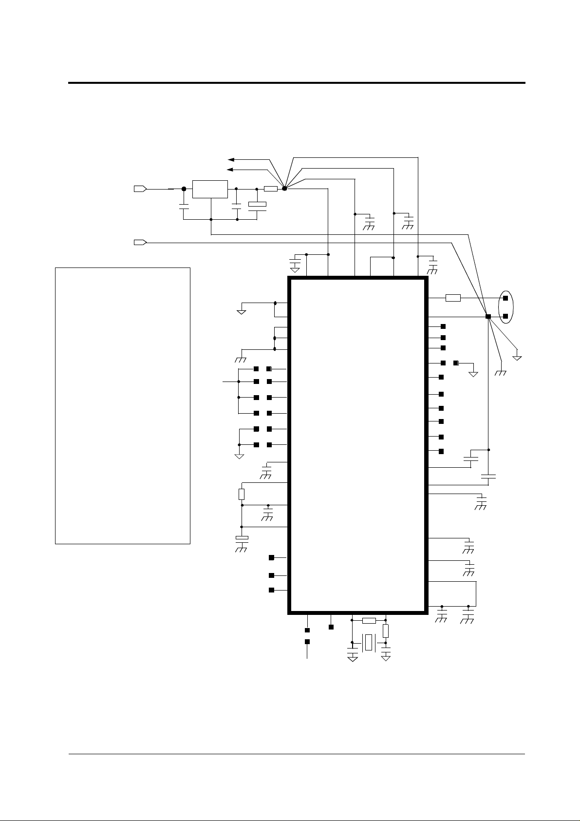
EXAMPLE SUPPORT CIRCUIT
AVD
VDD
8
REG1
+7 to +12v dc
0v
C1
2,3,
6,7
C2
Example Support Circuit
1
C3
R1
C5
C6
Component Value
IC1 VV5430
REG1 LM78L05
C1,C2 0.22 µF
C3 68 µF
(6V Tant.)
C4 - C9,C13, 0.1 µF
C15 - C19
C10 4.7µF
C11, C12 10 pF
C14 100pF
R1 5R6
R2 10R
R3 10M
R4 75R
R5 33R
X1 Crystal
CCIR:14.7456 MHz
EIA:12.0000 MHz
Preliminary
Use Surface Mount components
throughout.
VDD
R5
C10
C8
C9
SCL
SDA
C4
24
31
42
10
48
16
20
28
19
22
21
44
45
46
47
39
40
29
27
VSS1
VSS2
DVSS
AVSS
AGND
SAB1
SAB0
BKLIT
LIN
AGC
AEC
VBLOOM
VRT
VCM
VREF2V7
SCL
SDA
RESETB
CPE
35
41
34
VDD2VDD1
DVDD
IC1
(48 pin LCC)
VV5430
CKIN CKOUT
SIN
26
17
1
7
AVCC AVDD
VOFF/VPED
25
R3
R2
13
VVDD
AVO
VGND
SCI
LST
SCE
CCIR
FST
PVB
PV
ODD
AMP2
AMP1
EBCK
EVWT
VBLTW
DNC
DEC2V7
DEC2V2
VBG
14
38
30
18
23
33
32
37
12
8
43
6
5
4
15
36
3
2
C7
R4
11
C19
9
C13
MONITOR
C18
C17
C16
C15
C14
C11
VDD
C12
X1
1. Keep nodes Supply and Ground pi ns low impedance and independ ent
2. Video output should be referred to VGND.
3. Keep circuit components close to chip pins (especially de-coupling capacitors)
09/04/97 31
Page 32

VISION VV 5430 Sensor
VLSI VISION LIMITED
UK Office
Aviation House,
31 PInkhill,
Edinburgh, UK
EH12 7BF
Tel: +44 (0)131 539 7111
Fax: +44 (0)131 539 7140
Email: [email protected]
VLSI Visio n Lt d. res erv es the right to make changes to its pro ducts and specifications at any time. Information furnished by VISION is believed to be accurate, but no responsibility is ass um ed by VISION fo r t he use of said inf ormation, nor a ny inf ringemen ts of patents or of any other t hird party right s w hic h
may result f rom s aid use. No lice ns e is granted by implicati on or otherwis e
under an y pat ent or patent rights of any VI SION group co m pany.
USA West Office
18805 Cox Avenue,
Suite 260,
Saratoga,
California 95070, USA
Tel: +1 408 374 5323
Fax: +1 408 374 4722
Email: in fo @ v v l.co . uk
© Copyrigh t 1996, VLSI VI SI ON
liminar
USA East Office
2517 Highway 35
Bldg F, Suite 202
Manasquan
New Jersey 08736
Tel: +1 908 528 2222
Fax: +1 908 528 9305
Email: [email protected]
e
y
VLSI Vision agent or distributor
Pr
32 cd27033c.fm
 Loading...