

Page 1

cd38041a.fm 08/10/98 1
Commercial In Confidence
VV5409 is a highly-integrated CMOS camera with output
in 3 digital video formats:
1. 525 line, 60 fps - 306 x 244 image size -13. 5 M Hz or
14.31818 MHz crystals.
2. 625 line, 50 fps - 356 x 292 image siz e -13. 5 MHz or
17.734475 MHz crystal.
3. “VV6404 mode” - 356 x 292 image size .
VV5409 contains a two stage flash 8-bit analogue-todigital converter. Device set-up is fully automatic through
the CMOS sensor’s built in automatic black level
calibration algorithm.
The main features of the sensor’s digital interface are as
follows:
1. Tri-stateable 1 / 2 / 4 - wire output vi deo- data-b us for
8-bit video-data. Frame and line format information
is encoded within the video output data stream.
2. A 2-wire serial-interface for controlling the operation
of the sensor.
3. Data qualification clock, QCK (Tri-stateable)
4. Frame synchronisation signal, FST (Tri-stateable)
Exposure and gain values ar e progr ammed t hrough t he b idirectional 2-wire serial-interface.
• 525 line, 60 fps / 625 line, 50 fps output formats
• CCIR-601/656 compliant timing
• CIF Format Pixel-Array:
355 x 292 (306 x 244 for 525 line mode)
• Variable frame rate:
60/30/15/7.5 fps & 50/25/12.5/6.25 fps
• Crystals Supported:
13.5 MHz, 14.31818 MHz, and 35.46895 MHz
• On-chip 8-bit A/D convertor
• 1 / 2/ 4 - wire proprietary digital video bus
• 2-wire serial control interface
• Programmable exposure and gain values
• Automatic black level calibration
• Programmable inter line/frame timings
•Low power
• Standard 48 BGA and 48LCC Packages
• On-chip Audio pre-amp.
Pixel Resolution 306 x 244 or 356 x 292
Pixel Size 9.0 µm x 8.25 µm
Exposure control 25000:1 (performed by
host)
Format CIF
SNR TBD
Supply Voltage 5.0 V DC +/- 5%
Supply Current TBD
Operating
Temperature
Range
0
o
C - 40oC
Technology 0.6um 2-Level Metal CMOS
Package type 48BGA and 48LCC
TECHNICAL SPECIFICATION
GENERAL DESCRIPTION
CIF Format Monochrome Digital Image Sensor
VISION
VV5409 Digital CMOS Sens or
CUSTOMER DATASHEET (RESTRICTED)
CHARACTERISTICS
Important:
A host processor is required to perform Automatic Exposure and Gain control (AEC/AGC) via the sensor
serial interface, and to generate an appropriate video output timing format.
cd38041a.fm 08/10/98 2
VV5409 CMOS Monochrome Sensor Datasheet (Restricted)
Rev 1.0
Commercial In Confidence
Table of Contents
1. Introduction.....................................................................................................................................4
1.1 Typical applications ........................................................................................................................4
1.2 VV5409 overview ...........................................................................................................................4
1.3 Automatic Black Level Calibration..................................................................................................4
1.4 Exposure Control............................................................................................................................5
1.5 Digital Interface..............................................................................................................................5
1.6 System Reset.................................................................................................................................6
1.7 Startup configuration of Setup Data...............................................................................................6
1.8 Other Features.................. .............. .............. .............. ............................. .............. .............. ..........6
2. Operatin
g
Modes .................................................. ............... ............................ .............. .............. ...8
2.1 Video Timing.............. .............. .............. ............................. .............. .............. .............. .............. ...8
2.2 Pixel-Array.................... .............. .............. ............... ............................ .............. .............. ...............9
3. Automatic Black Level Calibration.............................................................................................. 11
4. Exposure Control.......... .............. .............. ............................. .............. .............. ...........................12
5. Di
g
ital Video Interface Format.....................................................................................................14
5.1 General description ......................................................................................................................14
5.2 Embedded control data ................................................................................................................15
5.3 Video timing reference and status/configuration data.................................................................. 17
5.4 Detection of sensor using data bus state.....................................................................................33
5.5 Resetting the Sensor Via the Serial Interface.............................................................................. 33
5.6 Power-up, Low-power and Sleep modes .....................................................................................33
5.7 Qualification of Output Data.........................................................................................................38
6. Serial Control Bus........................................................................................................................43
6.1 General Description......................................................................................................... ............. 43
6.2 Serial Communicati on Pro to co l........................ .............. .......................................... ............... .....43
6.3 Data Format.................................................................................................................................43
6.4 Message Interpretation................................................................................................................. 45
6.5 The Programmers Model..............................................................................................................45
6.6 Register descriptions....................................................................................................................47
6.7 Types of serial interface messages..............................................................................................58
6.8 Serial-Interfac e Ti mi n g............... .............. ............... .............. .......................................... ............. 62
7. Clock Si
g
nal..................................................................................................................................64
8. Synchronisin
g
Multiple Cameras................................................................................................65
9. Other Features ..............................................................................................................................67
9.1 Microphone Amplifier....................................................................................................................67
9.2 Debounced Switch Input . . ............................................................................................................68
9.3 Serial-Interface Programmable Pins ............................................................................................ 68
10. Detailed specifi cations................................................ ............... .............. ....................................69
11. Pinouts and pin descriptions.......................................................................................................70
11.1 Sensor pin list...............................................................................................................................70
11.2 48BGA pinout...............................................................................................................................72
11.3 48LCC Pinout............................................................................................................................... 73
12. Packa
g
e dimensions.............................. .............. ........................................... .............. .............. .74
Page 2
cd38041a.fm 08/10/98 3
VV5409 CMOS Monochrome Sensor Datasheet (Restricted)
Rev 1.0
Commercial In Confidence
12.1 48BGA (400G)......... ............... .............. .......................................... ............... ...............................74
12.2 48LCC.............. ........................................... .............. .............. ........................................... .......... 75
13. Su
gg
ested VV5409 support circuit..............................................................................................76
14. Evaluation kits (EVK’s).......................................................... .............. .............. ............... ............78
15. Orderin
g
details........................................................... ............... .............. ....................................78
Note
: In this document, where hexadecimal values are used, they are indicated by a subscript H, such as
FF
H
; other values are decimal.
cd38041a.fm 08/10/98 4
VV5409 CMOS Monochrome Sensor Datasheet (Restricted)
Rev 1.0
Commercial In Confidence
1. Introduction
The VV5409 is a highly integrated CMOS digital imaging sensor with 3 different digital video output formats.
The sensor contains a two-stage flash, 8-bit ADC (Analogue to Digital Converter). Exposure control can be
handled automatically by the host. Other device set-ups can be controlled using the 2-wire serial-interface.
1.1 Typical applications
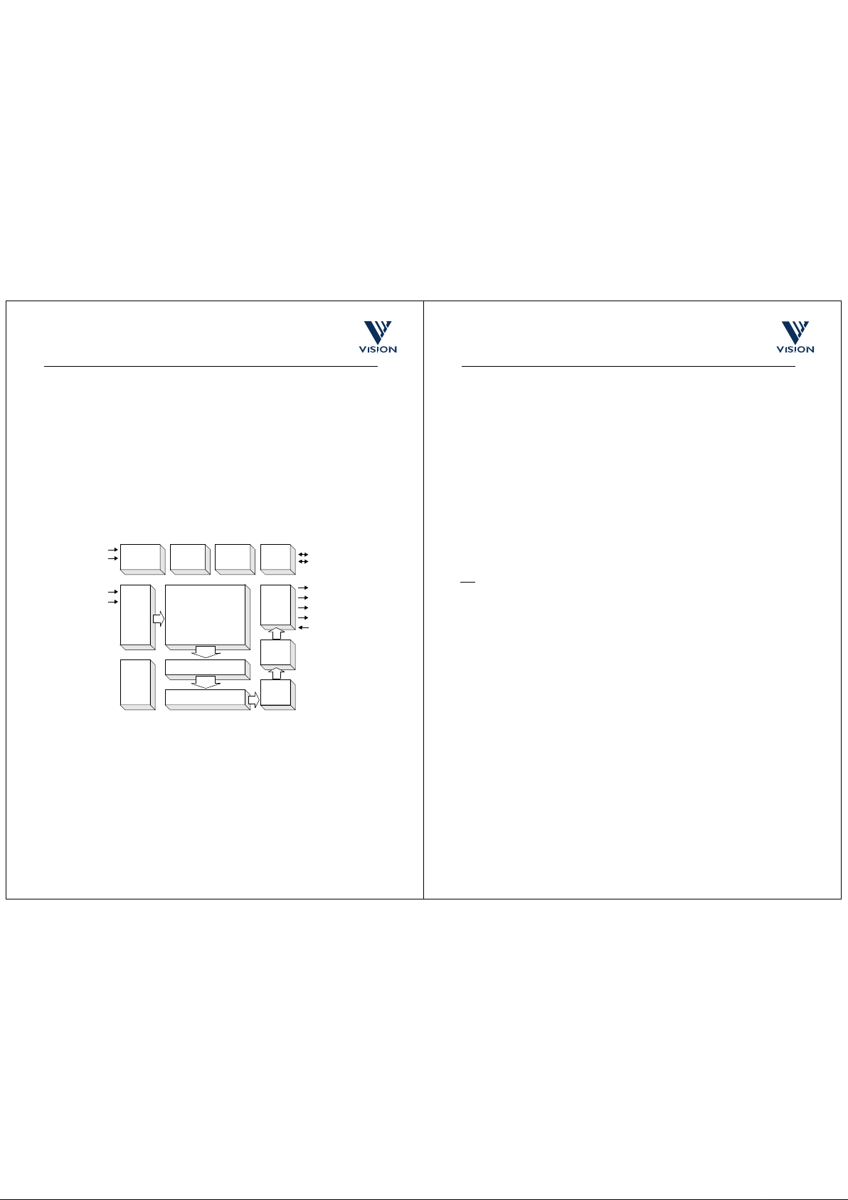
• Monochrome Video Surveillance/CCTV
• Biometrics
• Automotive
• Machine Vision
Figure 1.1 : Typical block diagram: Monochrome Video application
1.2 VV5409 overview
VV5409 is a CIF format CMOS image sensor which outputs digital pixel-data at frame and line rates
compatible with either NTSC or PAL video standards. Table 1.1 summarises the main video modes.
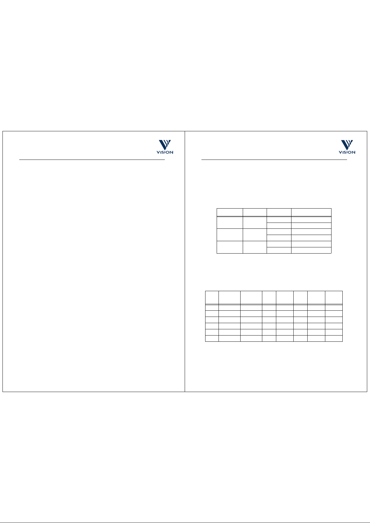
The pixel-data is digitised by an on-chip 8-bit ADC (Figure 1.2).
All of the video modes can be programmed through the serial-interface. The various operating modes are
detailed in Section 2.
Important:
The sensor’s video-data stream only contains raw pixel-data. An intelligent host co-processor is
required to perform auto-exposure and gain control, and to generate appropriate video output timing.
1.3 Automatic Black Level Calibration
Automatic black level control ensures consistent picture quality across the whole range of operating
conditions.
Mode
Clock
(MHz)
Pixel
Clock
Divisor
Image
Size
Line Time
(µs)
Lines
per
Frame
Frame
Rate
(fps)
CIF - 25 fps 7.15909 2 356 x 292 131.580969 304 24.99961
CIF - 30 fps 7.15909 2 356 x 292 109.790490 304 29.96137
PAL (656) 13.500000 2 356 x 292 64.000000 625 25.00000
NTSC (656) 13.500000 2 306 x 244 63.555564 525 29.97003
PAL (8 fsc) 35.46895 5 356 x 292 63.999639 625 25.00014
NTSC (8 fsc) 28.636360 5 306 x 244 63.555564 525 29.97003
Table 1.1 : Video Modes
- AEC/AG C
- Custom
VV5409
Camera
Head
409 clk
serial comm s
4-bit 409 video data
Host
controller
Video
Output
Custom
Video Output
Page 3
cd38041a.fm 08/10/98 5
VV5409 CMOS Monochrome Sensor Datasheet (Restricted)
Rev 1.0
Commercial In Confidence
1.4 Exposure Control
VV5409 does not include any form of automatic exposure and gain control. To produce a correctly exposed
image in the sensor-array, an exposure control algorithm must be implemented externally. This must be
performed by a host controller/co-processor.
1.5 Digital Interface
The sensor offers a very flexible digital interface, its main components are listed below:
1. A tri-stateable, 4-wire, data-bus (D[3:0]) for sending both video-data, and embedded timing references
2. A data qualification clock, QCK, which can be programmed through the serial-interface, to behave in a
number of different ways (Tri-stateable)
3. A line start signal, LST (Tri-stateable)
4. A frame start signal, FST (Tri-stateable)
5. OEB tri-states all 8 data-bus lines, D[7:0], the qualification clock, QCK, LST, and FST
6. The ability to synchronise the operation of multiple cameras
7. A 2-wire, serial-interface, (SDA,SCL) for controlling and setting up the device
1.5.1 Digital Data Bus
Along within the pixel-data, codes representing the start and end of fields and the start and end of lines are
embedded within the video-data stream to allow a host controller to synchronise with video-data the camera
module is generating. Section 5. defines the format for the output video-data stream.
The 8-bit data which makes up the video-data stream can be output on the data-bus in one of 3 ways:
1. A series pair of 4-bit nibbles, most significant nibble first, on 4-wires.
2. Four, 2-bit values, most significant 2-bit value first, on 2-wires.
3. Bit-serial data, eight 1-bit values, least significant bit first, on 1-wire.
For the 2, and 1-wire modes, the complement of the data can also be enabled in addition to the data itself.
SAMPLE & HOLD
HORIZONTAL SHIFT
PHOTO DIODE
ANALOG
VOLTAGE
REFS.
VERTICAL
SHIFT
REGISTER
8-bit
ADC
ARRAY
REGISTER
SERIAL
INTER-
FACE
Figure 1.2 : Block Diagram of VV5409 Image Sensor
OUTPUT
FORMAT
GAIN
IMAGE
FORMAT
BLACK
CALIBRATION
EXPOSURE
CONTROL
STAGE
D[3:0]
QCK
LST
FST
OEB
RESETB
SIN
SDA
SCL
CLKI
MODE
cd38041a.fm 08/10/98 6
VV5409 CMOS Monochrome Sensor Datasheet (Restricted)
Rev 1.0
Commercial In Confidence
1.5.2 Frame Grabber Control Signals
To complement the embedded control sequences, the data qualification clock (QCK), the line-start-signal
(LST) and the field-start-signal (FST), signals can independently be set-up to either be:
1. Disabled
2. Free-running
3. Qualify only the control sequences and the pixel-data
4. Qualify the pixel-data only.
There is also the choice of two different QCK frequencies where one is twice the frequency of the other.
1. Fast QCK: the falling edge of the clock qualifies every 4, 2 or 1-bit block of data that makes up a pixel
value.
2. Slow QCK: the rising edge qualifies the 1st, 3rd, 5th, etc. blocks of data which make up a pixel value,
while the falling edge qualifies the 2nd, 4th, 6th etc. blocks of data. For example, in the 4-wire mode,
the rising edge of the clock qualifies the most significant nibbles, while the falling edge of the clock
qualifies the least significant nibbles.
1.5.3 Synchronisation of Multiple Cameras
Multiple camera configurations can be synchronised by applying a rising edge to the SIN pins once per frame
(every second field).
The FST/DIN pin of the one of cameras (the master) can be re-configured as a SNO output to supply the
synchronidsation signal for the other cameras.
Note
: The SNO function has not been verified.
1.5.4 2-wire Serial-Interface
The 2-wire serial-interface provides complete control over how the sensor is setup and run. The sensor serial
address is fixed at 20
H
.
Two broadcast serial-interface addresses are supported. One allows all sensors to be written to in parallel,
and if a VISION co-processor is in use, the other allows all sensors and co-processors to be written to in
parallel.
Section 6. defines the serial-interface communications protocol, and the register map of all the locations
which can be accessed through the serial-interface.
1.6 System Reset
Using the RESETB pin (active low, internal pull-up), a System Reset of the sensor can be activated. The
sensor behaves exactly as if a power down then power up has taken place, i.e., all sensor serial registers are
reset to their default status, and video timing will be reset.
1.7 Startup configuration of Setup Data
The sensor should be correctly configured on power up, or following a System Reset (Section 1.6), , for
correct operation of the sensor, by writing settings to the camera registers on startup. This applies to the
Setup0 [16], Setup1 [17], and at1 [121] registers in particular.
1.8 Other Features
1.8.1 Microphone Pre-Amplifier
Pins AIN, and AOUT, are the input, and output respectively, for a 2-stage Microphone amplifier. The gain of
this amplifier is programmable through the serial-interface.
The output of the Microphone can be multiplexed at the end of a video line, onto the input of the 8-bit ADC
Page 4
cd38041a.fm 08/10/98 7
VV5409 CMOS Monochrome Sensor Datasheet (Restricted)
Rev 1.0
Commercial In Confidence
digitised pixel-data. This value is output, once per line, as part of the embedded “end-of-line” sequence.
While this amplifier is primarily intended as a Microphone amplifier, it can be used as way to digitise any
“slow-moving” analogue input. The maximum sample rate is approximately 15k samples/second as there is
only one sample per line of video. See also Section 9.1.
1.8.2 Debounced Switch Input
This de-bounced input (the FST/DIN pin re-configured as a debounced switch input pin) is designed for use
with a switch, for still-image capture. If the switch is pressed, it sets a flag in the status line for the next field,
marking it as the one the user has selected. See also Section 9.2.
cd38041a.fm 08/10/98 8
VV5409 CMOS Monochrome Sensor Datasheet (Restricted)
Rev 1.0
Commercial In Confidence
2. Operating Modes
2.1 Video Timing
The video format mode on power-up is determined by the value of bits 6-7 of the setup0 register. It may be
desirable to access a larger image array size by enabling PAL or NTSC video output modes. While the video
outout timing from the sensor is
compatible
with PAL.NTSC/CCIR656 formats, video sync timing and
encoding must be performed by an external host controller.
The frame/field rate is programmable only through the serial-interface. Setup0 bit 3 selects between 30 and
25 frames per second for the CIF modes, and 60/50 fields per second for the Digital, and Analog Timing
modes.
The number of video lines-in for each frame-rate, is the same (304) for each of the CIF modes. The slower
frame rate is implemented, by simply extending the line period from 393 pixel periods, to 471 pixel periods.
Table 2.2 details the setup for each of the video timing modes. Changing either the mode pin, or a serial write
to the
video_timing
register will force the contents of other registers in the serial-interface to change to the
appropriate values. If, for example, a different data output-mode is required from the default, for a particular
video mode, a write to the appropriate register after the mode has changed will setup the desired value.
For flexibility, the number of pixel clocks per line, and the number of lines per field, can be programmed
through the serial-interface, both to a maximum value of 510.
Video Mode setup0[6-7] setup0 Bit3 Video Mode
CIF (VV6404) 00
2
0 CIF - 25 fps
1 CIF - 30 fps
DIGITAL (CCIR) 01
2
0 PAL (656)
1 NTSC (656)
ANALOG (TV) 10
2
0 PAL (8 fsc)
1 NTSC (8 fsc)
Table 2.1 : Video Timing Mode Select Pins
Mode Video Mode
Clock
(MHz)
Pixel
Clock
Divisor
Video
Data
Line
Length
Field
Length
Data
Output
Mode
0 CIF - 25 fps 7.15909 2 356 x 292 471 304 4-wire
1 CIF - 30 fps 7.15909 2 356 x 292 393 304 4-wire
2 PAL(656) 13.500000 2 356 x 292 432 312/313 4-wire
3 NTSC (656) 13.500000 2 306 x 244 429 262/263 4-wire
4 PAL (8 fsc) 28.636360 5 356 x 292 454 312/313 4-wire
5 NTSC (8 fsc) 35.46895 5 306 x 244 364 262/263 4-wire
Table 2.2 : Video Timing Modes
Page 5

cd38041a.fm 08/10/98 9
VV5409 CMOS Monochrome Sensor Datasheet (Restricted)
Rev 1.0
Commercial In Confidence
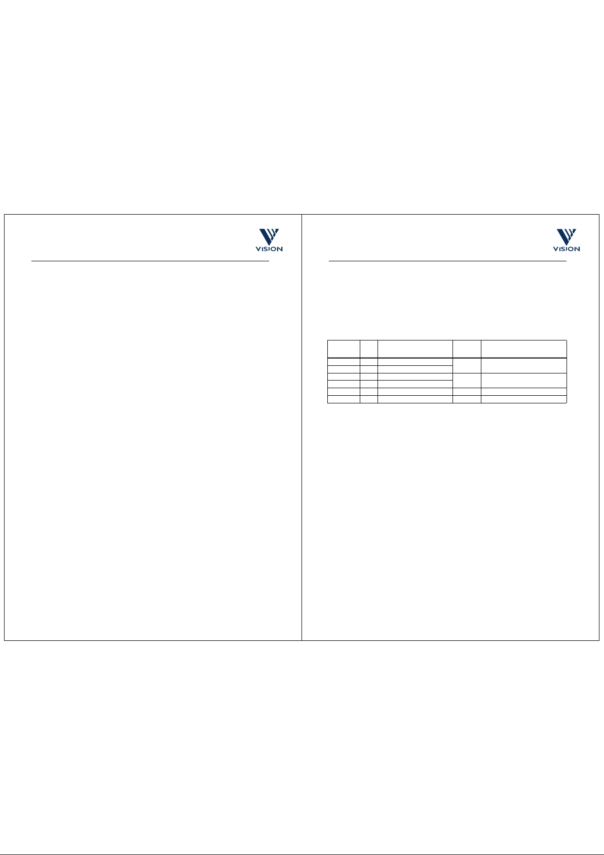
2.2 Pixel-Array
The physical pixel-array is 360 x 292 pixels. The pixel size is 9.0µm by 8.25 µm. The useable image size for
NTSC format is 302 x 240 pixels while for PAL and CIF formats it is 352 x 288 pixels. An optional border 2
pixels deep on all 4 sides of the array can be enabled (Figure 2.3). The resulting image sizes are 306 x 244
for NTSC, and 356 x 292 pixels for PAL and CIF video modes.The border option is programmable through
the serial-interface.
Figure 2.2 shows how the 302 x 240 sub-array is aligned within the bigger 352 x 288 pixel-array.The position
of the 306 x 244 sub-array has been offset by one column, relative to central location. Image read-out is noninterlaced raster scan. The larger 352 x 288 array covers pixels 4-355 and 2-289.
With extra border rows/columns enabled, and Figure 2.3 shows the relative array positions.
Note
: To enable correct readout of sensor pixels, bit 7 of the Setup1 register [17] must be set to 0. Its default
power-up value is 1.
Figure 2.1 : VV5409 Image format with border rows/columns disabled
Video Modes Border
Output Image size
(column x row)
NTSC Disabled 302 x 240
Enabled 306 x 244
PAL, CIF Disabled 352 x 288
Enabled 356 x 292
Table 2.3 : Image Format Selection
302 Pixels
352 Pixels
240 Pixels
288 Pixels
4, 5, 6, 7, 8, 9, ...
..., 352, 353, 354, 355
26 Pixels
24 Pixels
2, 3, 4, 5, 6, 7, ...
..286, 287., 288, 289
24 Pixels
24 Pixels
cd38041a.fm 08/10/98 10
VV5409 CMOS Monochrome Sensor Datasheet (Restricted)
Rev 1.0
Commercial In Confidence
Figure 2.3 : VV5409 Image format with border rows/columns enabled
356 Pixels
360 Pixels
306 Pixels
302 Pixels
352 Pixels
240 Pixels
244 Pixels
288 Pixels
292 Pixels
0, 1, 2, 3, 4, 5,...
..., 355, 356, 358, 359
0, 1, 2, 3, 4, 5,...
..., 288, 289, 290, 291
24 Pixels
22 Pixels
22 Pixels22 Pixels
3210
1
3
2
0
54
289
291
290
288
357
356
355
354
359
358
Page 6
cd38041a.fm 08/10/98 11
VV5409 CMOS Monochrome Sensor Datasheet (Restricted)
Rev 1.0
Commercial In Confidence
3. Automatic Black Level Calibration
Black calibration is used to remove voltage offsets that cause shifts in the black level of the video signal.
VV5409 is equipped with an automatic function that continually monitors the output black level and calibrates
if it has moved out of range. The signal is corrected using two “Black-Calibration” DACs:
1. ADC stage DAC, B0[7:0].
2. OSA Input Offset Compensation DAC, B1 [7:0]
Black calibration can be split into two stages,
monitor
and
update
. During the monitor phase the current
black level of 4 black reference lines at the top of the pixel array is compared against two threshold values.
If the current value falls outside the threshold window then an update cycle is triggered. The update cycle can
also be triggered by a change in the gain applied to sensor core or via the serial interface (see also Section
6.6.5).
cd38041a.fm 08/10/98 12
VV5409 CMOS Monochrome Sensor Datasheet (Restricted)
Rev 1.0
Commercial In Confidence
4. Exposure Control
The exposure time for a pixel and the gain of the input amplifier to the 8-bit ADC are programmable via the
serial interface. The explanation below assumes that the gain and exposure values are updated together as
part of a 5 byte serial interface auto-increment sequence.
The exposure is divided into 2 components - coarse and fine. The coarse exposure value sets the number of
lines a pixel exposes for, while the fine exposure sets the number of additional pixel clock cycles a pixel
integrates for. The sum of the two gives the overall exposure time for the pixel array.
Exposure Time = Clock Divider Ratio x (Coarse x Line Length + Fine) x (CLKI clock period)
If an exposure value is loaded outwith the valid ranges listed in the above table the value is clipped to lie
within the above ranges.
Exposure and gain values are re-timed within the sensor to ensure that a new set of values is only applied to
the sensor array at the start of each frame. Bit 0 of the Status Register is set high when a new exposure value
is written via the serial interface but has not yet been applied to the sensor array.
There is a 1 frame latency between a new exposure value being applied to the sensor array and the results
of the new exposure value being read-out. The same latency does not exist for the gain value. To ensure that
the new exposure and gain values are aligned up correctly the sensor delays the application of the new gain
value by one frame relative to the application of the new exposure value.
To eliminate the possibility of the sensor array seeing only part of the new exposure and gain setting, if the
serial interface communications extends over a frame boundary, the internal re-timing of exposure and gain
data is disabled while writing data to any location in the Exposure page of the serial interface register map.
Thus if the 5 bytes of exposure and gain data is sent as an auto-increment sequence, it is not possible for
the sensor to consume only part of the new exposure and gain data.
See also Section 6.6.3.
Register
Index
Bits Function Default Comment
32 0:0 Fine MSB exposure value 0 Maximum Line Length Mode
Dependant
33 7:0 Fine LSB exposure value
34 0:0 Coarse MSB exposure value 302 Maximum equals Field Length-1.
35 7:0 Coarse LSB exposure value
36 3:0 Gain value 0
37 1:0 Clock divisor value 0
Table 4.1 : Exposure, Clock Rate and Gain Registers
Page 7
cd38041a.fm 08/10/98 13
VV5409 CMOS Monochrome Sensor Datasheet (Restricted)
Rev 1.0
Commercial In Confidence
Gain Binary code Actual signal gain Gain Binary code Actual signal gain
0000
2
0.500 1000
2
0.533
0001
2
1.000 1001
2
1.143
0010
2
0.667 1010
2
0.727
0011
2
2.000 1011
2
2.667
0100
2
0.571 1100
2
0.615
0101
2
1.333 1101
2
1.600
0110
2
0.8 00 1110
2
0.889
0111
2
4.0 00 1111
2
8.000
Table 4.2 : System Analog Gain Values
Clock Divisor Setting Pixel Clock Divisor
00
2
2
01
2
4
10
2
8
11
2
16
Table 4.3 : Clock Divisor Values
cd38041a.fm 08/10/98 14
VV5409 CMOS Monochrome Sensor Datasheet (Restricted)
Rev 1.0
Commercial In Confidence
5. Digital Video Interface Format
5.1 General description
The video interface consists of a unidirectional, tri-stateable 4-wire data-bus. The nibble transmission is
synchronised to the rising edge of the system clock.
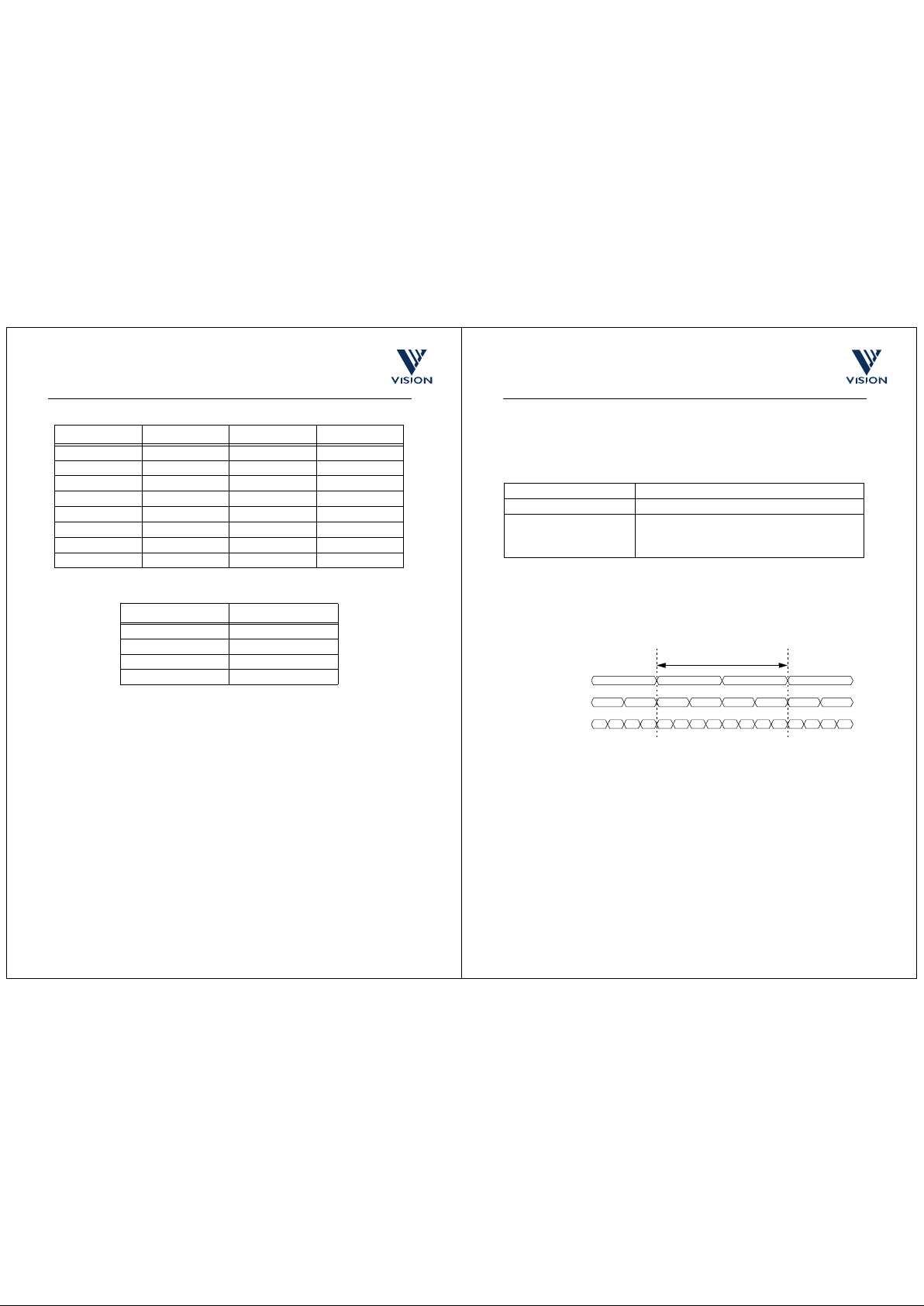
Digital video-data is 8 bits per sample, and can be transmitted in one of three ways:
1. A series pair of 4-bit nibbles, most significant nibble first, on 4-wires
2. Four 2-bit values, most significant 2-bit value first, on 2-wires
3. Bit-serial data, eight 1-bit values, least significant bit first, on 1-wire.
In the following description the 4-wire mode is used as an example. The 2-wire, and 1-wire modes can be
viewed as variants of the 4-wire mode.
Control information is multiplexed with the sampled pixel-data. Such control information includes both video
timing references, sensor status/configuration data and digitised values for VV5409’s analogue input pin,
AIN.
Video timing reference information takes the form of field start characters, line start characters, end of line
characters and a line counter.
Read-out Order Progressive Scan (Non-interlaced)
Form of encoding Uniformly quantised, PCM, 8 bits per sample
Correspondence between video
signal levels and quantisation
levels:
Internally valid pixel-data is clipped to ensure that 00
H
and FFH
values do not occur when pixel-data is being output on the databus. This gives 254 possible values for each pixel (1 - 254). The
video black level corresponds to code 16.
Table 5.1 : Video encoding parameters
Figure 5.1 :
4-wir
e, 2-wire and 1-wire Output Modes
4 - wire Output Mode
2 - wire Output Mode
1 - wire Output Mode
D
7,D6
D
7
D
5,D4D3,D2D1,D0
D6D5D4D3D2D1D
0
D
7,D6,D5,D4
D
3,D2,D1,D0
D
7,D6
D
1,D0
D7D
6
D0D
1
D
5,D4
D
3,D2
D
3,D2,D1,D0
D
7,D6,D5,D4
D5D
4
D3D
2
8-bit pixel-data
Page 8

cd38041a.fm 08/10/98 15
VV5409 CMOS Monochrome Sensor Datasheet (Restricted)
Rev 1.0
Commercial In Confidence
5.2 Embedded control data
To distinguish the control data from the sampled video data all control data is encapsulated in embedded
control sequences. These are 6 bytes long and include a combined escape/sync character, 1 control byte
(the ‘command byte’) and 2 bytes of supplementary data.
To minimise the susceptibility of the embedded control data to random bit errors redundant coding
techniques have been used to allow single bit errors in the embedded control words to be corrected.
However, more serious corruption of control words or the corruption of escape/sync characters cannot be
tolerated without loss of sync to the data stream. To ensure that a loss of sync is detected a simple set of
rules has been devised. The four exceptions to the rules are outlined below:
1. Data containing a command words that has two bit errors.
2. Data containing two ‘end of line’ codes that are not separated by a ‘start of line’ code.
3. Data preceding an ‘end of field’ code before a start of frame’ code has been received.
4. Data containing line that do not have sequential line numbers (excluding the ‘end of field’ line).
If the video processor detects one of these violations then it should abandon the current field of video
5.2.1 The combined escape and sync character
Each embedded control sequence begins with a combined escape and sync character that is made up of
three words. The first two of these are FF
H
FFH- constituting two words that are illegal in normal data. The
next word is 00
H
- guaranteeing a clear signal transition that allows a video processor to determine the
position of the word boundaries in the serial stream of nibbles. Combined escape and sync characters are
always followed by a command byte - making up the four byte minimum embedded control sequence.
5.2.2 The command word
The byte that follows the combined escape/sync characters defines the type of embedded control data. Three
of the 8 bits are used to carry the control information, four are ‘parity bits’ that allow the video processor to
detect and correct a certain level of errors in the transmission of the command words, the remaining bit is
always set to 1 to ensure that the command word is never has the value 00
H
. The coding scheme used allows
the correction of single bit errors (in the 8-bit sequence) and the detection of 2 bit errors The three data bits
of the command word are interpreted as shown in Figure 5.2.The even parity bits are based on the following
relationships:
1. An even number of ones in the 4-bit sequence (C
2
, C1, C0 and P0).
2. An even number of ones in the 3-bit sequence (C
2
, C1, P1).
3. An even number of ones in the 3-bit sequence (C
2
, C0, P2).
4. An even number of ones in the 3-bit sequence (C
1
, C0, P3).
Table 5.3 shows how the parity bits maybe used to detect and correct 1-bit errors and detect 2-bit errors.
5.2.3 Supplementary Data
The last 2 bytes of the embedded control sequence contains supplementary data. Three options:
1. The current 12-bit line number. The 12-bit line number is packaged up by splitting it into two 6-bit values. Each 6-bit values is then converted into an 8-bit value by adding a zero to the start and an odd
word parity bit at the end.
2. If the line code equals the end of line, the 2 bytes are padded out using null characters (FF
H
).
3. If the line code equals the end of line and digitise analogue input enabled then the 2 supplementary
data bytes contain 2 8-bit values representing the values of the analogue input at those two points in
time.
cd38041a.fm 08/10/98 16
VV5409 CMOS Monochrome Sensor Datasheet (Restricted)
Rev 1.0
Commercial In Confidence
Line Code Nibble XH (1 C2 C1 C0) Nibble YH (P3 P2 P1 P0)
End of Line 10002 (8H) 00002 (0H)
Table 5.2 : Embedded Line Codes
Figure 5.2 :
Embedded Control Sequence
Command
(Line Code)
Supplementary Data
(i) Line Number (L
11
MSB)
or
(ii) If Line Code = End of Line then
Odd
word
parity
01234567
Bit
Nibble D2 = FHNibble D3 = FHNibble D0 = FHNibble D1 = F
H
11 1 1
L110 L10L9L7L8L6P
A6A7A5A4A2A3A1A
0
11 1 1 11 1 1 11 1 1
Nibble D2Nibble D
3
01234567
Bit
L50 L4L3L1L2L0P
Nibble D0Nibble D
1
B6B7B5B4B2B3B1B
0
Nibble D2Nibble D3Nibble D0Nibble D
1
or
(iii) If Line Code = End of Line and digitise analogue input enabled then
01234567
Bit
C21 C1C0P2P3P1P
0
Nibble YHNibble X
H
4-wire output
mode
8-bit Data
Escape/Sync Sequence
D0D1D2D3YHXH0H0HFHFHFHF
H
FFHFFH00HXY
HD3D2D1D0
Page 9

cd38041a.fm 08/10/98 17
VV5409 CMOS Monochrome Sensor Datasheet (Restricted)
Rev 1.0
Commercial In Confidence
5.3 Video timing reference and status/configuration data
Each frame of video sequence is made up of 2 fields. Each field of data is constructed of the following
sequence of data-lines.
1. A start-of-field line
2. 2 ‘black lines’ (used for black level calibration)
3. A number of blank lines
4. A number active video lines
5. An end of field line
6. A number of blank lines.
Blank Line (BL) 1001
2 (9H
) 11012 (DH)
Black line (BK) 1010
2 (AH
) 10112 (BH)
Visible Line (VL) 1011
2 (BH
)0110
2
(6H)
Start of Even Field (SOEF) 1100
2 (CH
) 01112 (7H)
End of Even Field (EOEF) 1101
2 (DH
)1010
2
(AH)
Start of Odd Field (SOOF) 1110
2 (EH
) 11002 (CH)
End of O dd Fi eld (EO OF ) 1111
2 (FH
) 00012 (1H)
Parity Checks
Comment
P
3
P
2
P
1
P
0
4444
Code word un-corrupted
4448
P
0
corrupted, line code OK
4484
P
1
corrupted, line code OK
4844
P
2
corrupted, line code OK
8444
P
3
corrupted, line code OK
8848
C
0
corrupted, invert sense of C
0
8488
C
1
corrupted, invert sense of C
1
4888
C
2
corrupted, invert sense of C2
All other codes 2-bit error in code word.
Table 5.3 : Detection of 1-bit and 2-bit errors in the Command Word
Line Code Nibble X
H
(1 C2 C1 C0) Nibble YH (P3 P2 P1 P0)
Table 5.2 : Embedded Line Codes
cd38041a.fm 08/10/98 18
VV5409 CMOS Monochrome Sensor Datasheet (Restricted)
Rev 1.0
Commercial In Confidence
Table 5.4 details the number of each type of data-lines for NTSC, PAL and CIF output formats when the
border rows and columns, are output, and not output, on the data-bus.
Each line of data starts with an embedded control sequence, which identifies the line type (as outlined in
Table 5.2). The control sequence is then followed by two bytes which, except in the case of the end-of-frame
line, contain a coded line number. The line number sequences starts with the start-of-frame line at 00
H,
and
increments, one per line, until the end-of-frame line. Each line is terminated with an end-of-line embedded
control sequence. The line start embedded sequences, must be used to recognise data-lines, as a number
of null bytes may be inserted between data-lines.
5.3.1 Blank lines
In addition to padding between data-lines, actual blank data-lines may appear in the positions indicated
above. These lines begin with start-of-blank-line embedded control sequences, and are constructed
identically to active video lines except that they will contain only blank bytes (07
H
).
5.3.2 Black line timing
The black lines (which are used for black level calibration) are identical in structure to valid video lines except
that they begin with a start-of-black line sequence and contain either information from the sensor ‘black lines’
or blank bytes (07
H
).
Video Format NTSC PAL CIF
Border Lines On Off On Off On Off
1st Field
Start-of-field Line 1 1 1 1 1 1
Black Lines 222222
Blanking Lines 7 9 7 9 7 9
Active Video lines 244 240 292 288 292 288
End of Field Line 1 1 1 1 1 1
Blanking Lines 7 9 9 11 1 3
Total 262 262 311 311 304 304
2nd Field
Start-of-field Line 1 1 1 1 1 1
Black Lines 222222
Blanking Lines 7 9 7 9 7 9
Active Video lines 244 240 292 288 292 288
End of Field Line 1 1 1 1 1 1
Blanking Lines 8 10 10 12 1 3
Total 263 263 312 312 304 304
Table 5.4 : Field and Frame Formats
Page 10

cd38041a.fm 08/10/98 19
VV5409 CMOS Monochrome Sensor Datasheet (Restricted)
Rev 1.0
Commercial In Confidence
Figure 5.3 : NTSC Field and Frame Formats - Borders On, Extra Black Lines Off
8 Blanking Lines
263
2 Black Lines
Start Of 2nd Field Line
End Of 2nd Field Line
7 Blanking Lines
244 Visible Lines
8 Blanking Lines
0
2nd Field = 263 Lines
Frame = 525 Lines
1
0
2
3
9
10
11
253
251
252
12
254
263
255
2 Black Lines
Start Of 1st Field Line
End Of 1st Field Line
7 Blanking Lines
244 Visible Lines
7 Blanking Lines
1st Field = 262 Lines
1
0
2
3
9
10
11
253
251
252
12
254
262
255
Start Of 1st Field Line
8
8
cd38041a.fm 08/10/98 20
VV5409 CMOS Monochrome Sensor Datasheet (Restricted)
Rev 1.0
Commercial In Confidence
Figure 5.4 : NTSC Field and Frame Formats - Borders On, Extra Black Lines On
8 Blanking Lines
263
8 Black Lines
Start Of 2nd Field Line
End Of 2nd Field Line
Blanking Line
244 Visible Lines
8 Black Lines
0
2nd Field = 263 Lines
Frame = 525 Lines
1
0
2
3
9
1011253
251
25212254
263
255
8 Black Lines
Start Of 1st Field Line
End Of 1st Field Line
Blanking Line
244 Visible Lines
7 Black Lines
1st Field = 262 Lines
1
0
2
3
9
1011253
251
25212254
262
255
Start Of 1st Field Line
8
8
Page 11
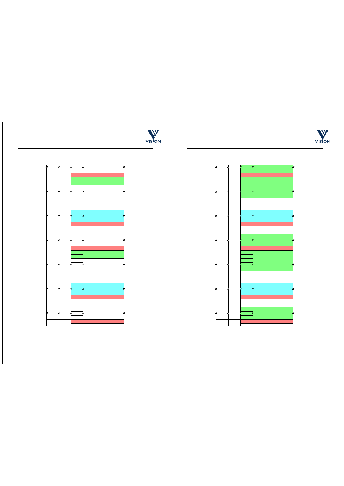
cd38041a.fm 08/10/98 21
VV5409 CMOS Monochrome Sensor Datasheet (Restricted)
Rev 1.0
Commercial In Confidence
Figure 5.5 : NTSC Field and Frame Formats - Borders Off, Extra Black Lines Off
10 Blanking Lines
263
2 Black Lines
Start Of 2nd Field Line
End Of 2nd Field Line
9 Blanking Lines
240Visible Lines
10 Blanking Lines
0
2nd Field = 263 Lines
Frame = 525 Lines
1
0
2
3
9
10
11
253
251
252
12
254
263
255
2 Black Lines
Start Of 1st Field Line
End Of 1st Field Line
9 Blanking Lines
240 Visible Lines
9 Blanking Lines
1st Field = 262 Lines
1
0
2
3
9
10
11
253
251
252
12
254
262
255
Start Of 1st Field Line
8
8
cd38041a.fm 08/10/98 22
VV5409 CMOS Monochrome Sensor Datasheet (Restricted)
Rev 1.0
Commercial In Confidence
Figure 5.6 :
NTSC Field and Frame Fo
rmats - Borders Off, Extra Bl
ack Lines On
8 Blanking Lines
263
8 Black Lines
Start Of 2nd Field Line
End Of 2nd Field Line
3 Blanking Lines
240 Visible Lines
8 Black Lines
0
2nd Field = 263 Lines
Frame = 525 Lines
1
0
2
3
9
1011253
251
25212254
263
255
8 Black Lines
Start Of 1st Field Line
End Of 1st Field Line
240 Visible Lines
7 Black Lines
1st Field = 262 Lines
1
0
2
3
9
1011253
251
25212254
262
255
Start Of 1st Field Line
8
8
2 Blanking Lines
3 Blanking Lines
2 Blanking Lines
Page 12
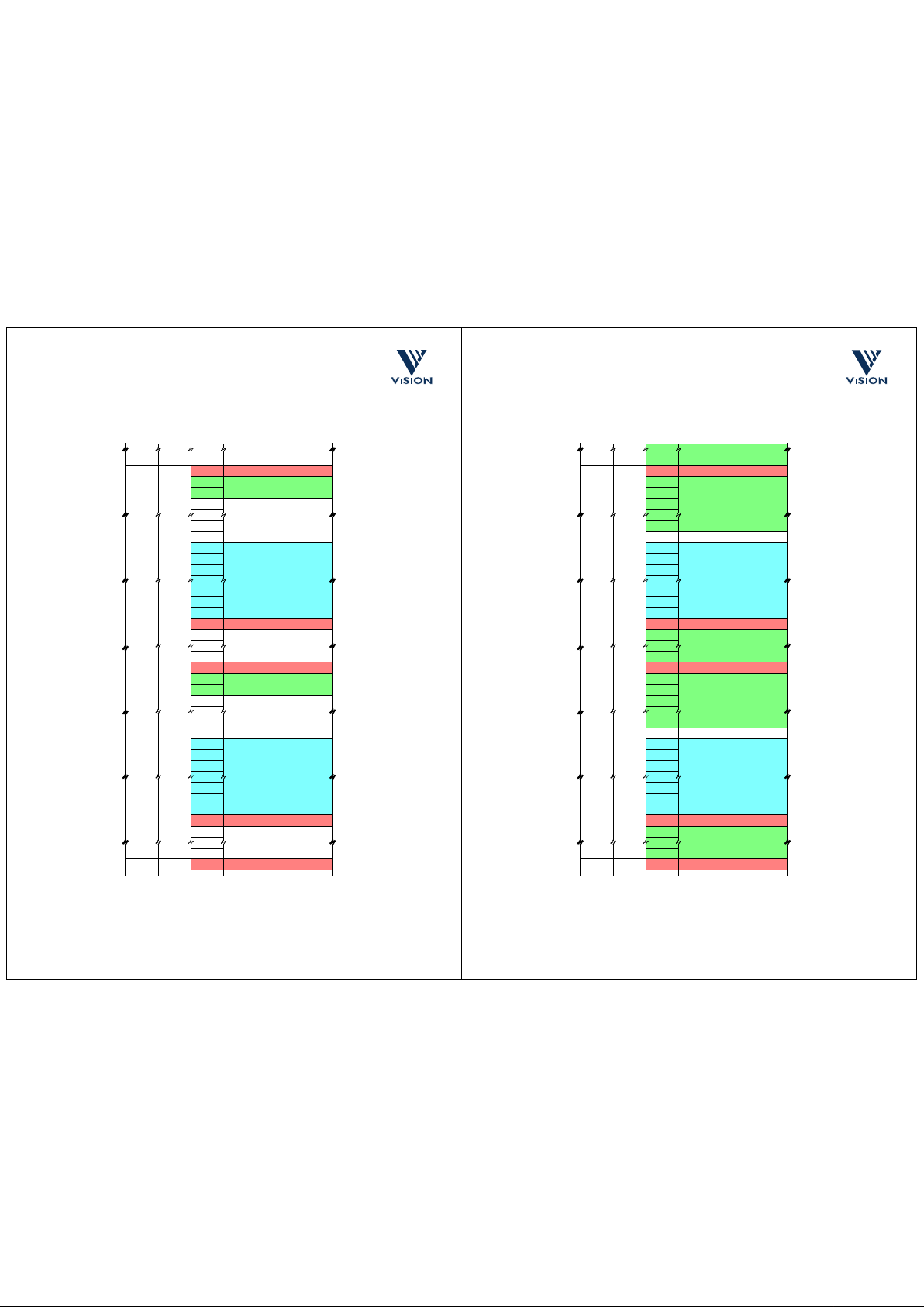
cd38041a.fm 08/10/98 23
VV5409 CMOS Monochrome Sensor Datasheet (Restricted)
Rev 1.0
Commercial In Confidence
Figure 5.7 : PAL Field and Frame Formats - Borders On, Extra Black Lines Off
10 Blanking Lines
312
2 Black Lines
Start Of 2nd Field Line
End Of 2nd Field Line
7 Blanking Lines
292 Visible Lines
10 Blanking Lines
0
2nd Field = 313 Lines
Frame = 625 Lines
1
0
2
3
9
10
11
301
299
300
12
302
312
303
2 Black Lines
Start Of 1st Field Line
End Of 1st Field Line
7 Blanking Lines
292 Visible Lines
9 Blanking Lines
1st Field = 312 Lines
1
0
2
3
9
10
11
301
299
300
12
302
311
303
Start Of 1st Field Line
8
8
cd38041a.fm 08/10/98 24
VV5409 CMOS Monochrome Sensor Datasheet (Restricted)
Rev 1.0
Commercial In Confidence
Figure 5.8 : PAL Field and Frame Formats - Borders On, Extra Black Lines On
10 Black Lines
312
8 Black Lines
Start Of 2nd Field Line
End Of 2nd Field Line
Blanking Line
292 Visible Lines
10 Black Lines
0
2nd Field = 313 Lines
Frame = 625 Lines
1
0
2
3
9
1011301
299
30012302
312
303
8 Black Lines
Start Of 1st Field Line
End Of 1st Field Line
Blanking Line
292 Visible Lines
9 Black Lines
1st Field = 312 Lines
1
0
2
3
9
1011301
299
30012302
311
303
Start Of 1st Field Line
8
8
Page 13
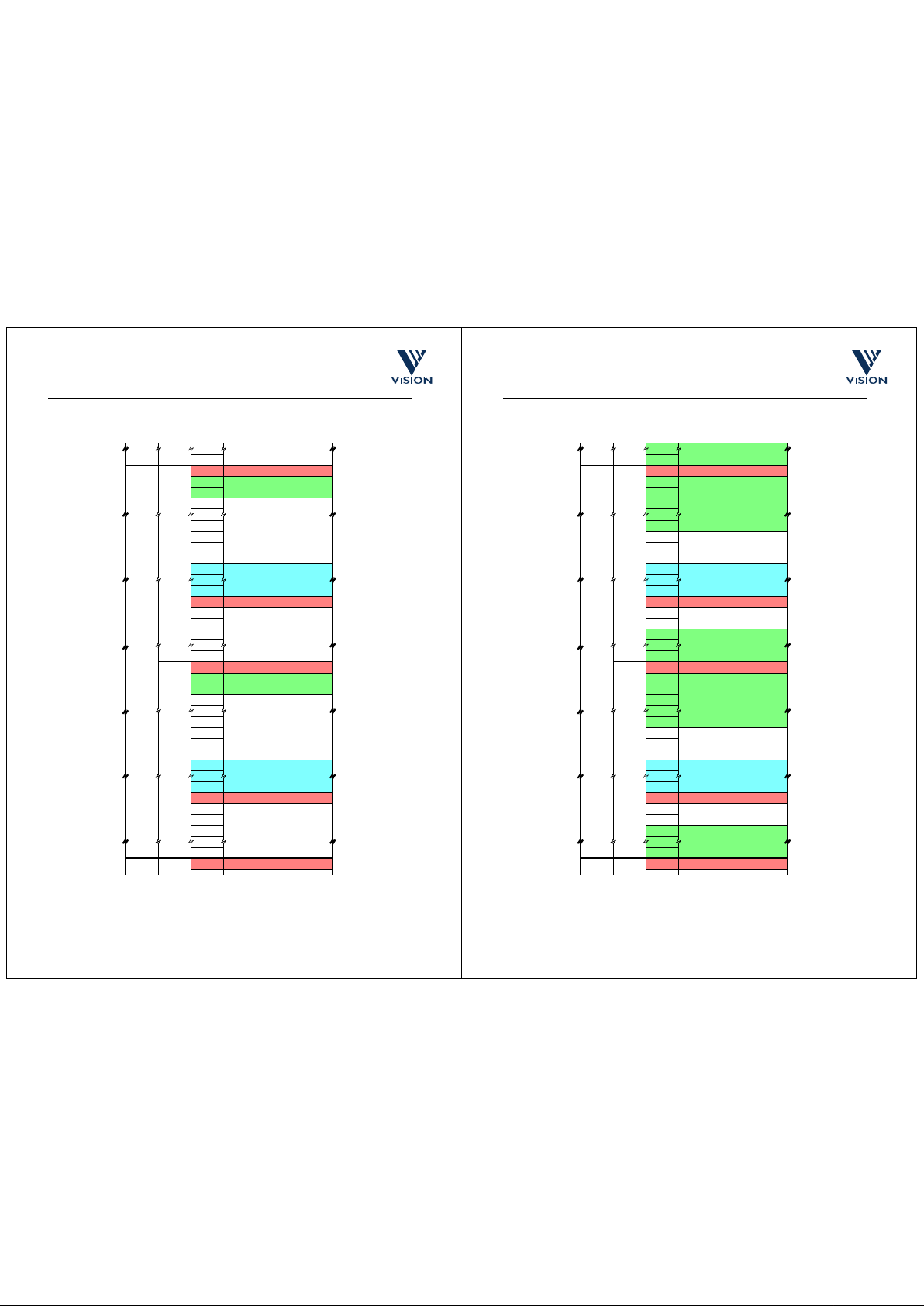
cd38041a.fm 08/10/98 25
VV5409 CMOS Monochrome Sensor Datasheet (Restricted)
Rev 1.0
Commercial In Confidence
Figure 5.9 : PAL Field and Frame Formats - Borders Off, Extra Black Lines Off
12 Blanking Lines
312
2 Black Lines
Start Of 2nd Field Line
End Of 2nd Field Line
9 Blanking Lines
288 Visible Lines
12 Blanking Lines
0
2nd Field = 313 Lines
Frame = 625 Lines
1
0
2
3
9
10
11
301
299
300
12
302
312
303
2 Black Lines
Start Of 1st Field Line
End Of 1st Field Line
9 Blanking Lines
288 Visible Lines
11 Blanking Lines
1st Field = 312 Lines
1
0
2
3
9
10
11
301
299
300
12
302
311
303
Start Of 1st Field Line
8
8
cd38041a.fm 08/10/98 26
VV5409 CMOS Monochrome Sensor Datasheet (Restricted)
Rev 1.0
Commercial In Confidence
Figure 5.10 :
PAL Field and Frame F
ormats - Borders Off, Extra Black Lines On
10 Black Lines
312
8 Black Lines
Start Of 2nd Field Line
End Of 2nd Field Line
3 Blanking Lines
288 Visible Lines
10 Black Lines
0
2nd Field = 313 Lines
Frame = 625 Lines
1
0
2
3
9
1011301
299
30012302
312
303
8 Black Lines
Start Of 1st Field Line
End Of 1st Field Line
3 Blanking Lines
288 Visible Lines
9 Black Lines
1st Field = 312 Lines
1
0
2
3
9
1011301
299
30012302
311
303
Start Of 1st Field Line
8
8
2 Blanking Lines
2 Blanking Lines
Page 14
cd38041a.fm 08/10/98 27
VV5409 CMOS Monochrome Sensor Datasheet (Restricted)
Rev 1.0
Commercial In Confidence
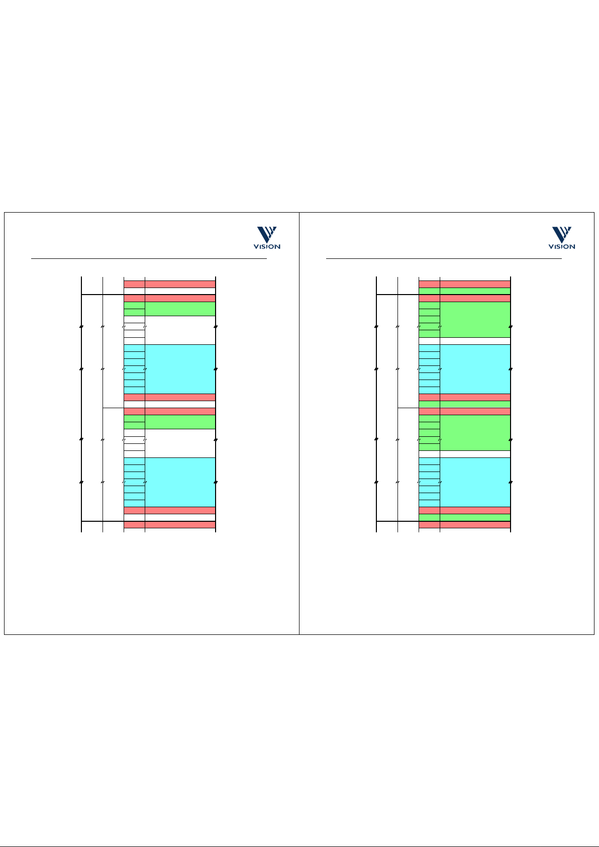
Figure 5.1 1 : CIF Field and Frame Formats - Borders On, Ext ra Bla ck L i nes Off
0
Frame = 608 Lines
Start Of 1st Field Line
2 Black Lines
Start Of 1st Field Line
End Of 1st Field Line
7 Blanking Lines
292 Visible Lines
Blankin
g
Line
1st Field = 304 Lines
1
0
2
3
9
10
11
301
299
300
12
302
303
8
End Of 2nd Field Line
Blanking Line
302
303
2 Black Lines
Start Of 1st Field Line
End Of 1st Field Line
7 Blanking Lines
292 Visible Lines
Blankin
g
Line
2nd Field = 304 Lines
1
0
2
3
9
10
11
301
299
300
12
302
303
8
cd38041a.fm 08/10/98 28
VV5409 CMOS Monochrome Sensor Datasheet (Restricted)
Rev 1.0
Commercial In Confidence
Figure 5.12 : CIF Field and Fr am e Fo rmat s - B o rder s On, Ext ra Black L ine s On
0
Frame = 608 Lines
Start Of 1st Field Line
8 Black Lines
Start Of 1st Field Line
End Of 1st Field Line
Blanking Line
292 Visible Lines
Black Line
2nd Field = 304 Lines
1
0
2
3
9
10
11
301
299
30012302
30388 Black Lines
Start Of 1st Field Line
End Of 1st Field Line
Blanking Line
292 Visible Lines
Black Line
1st Field = 304 Lines
1
0
2
3
9
1011301
299
30012302
3038End Of 2nd Field Line
Black Line
302
303
Page 15
cd38041a.fm 08/10/98 29
VV5409 CMOS Monochrome Sensor Datasheet (Restricted)
Rev 1.0
Commercial In Confidence
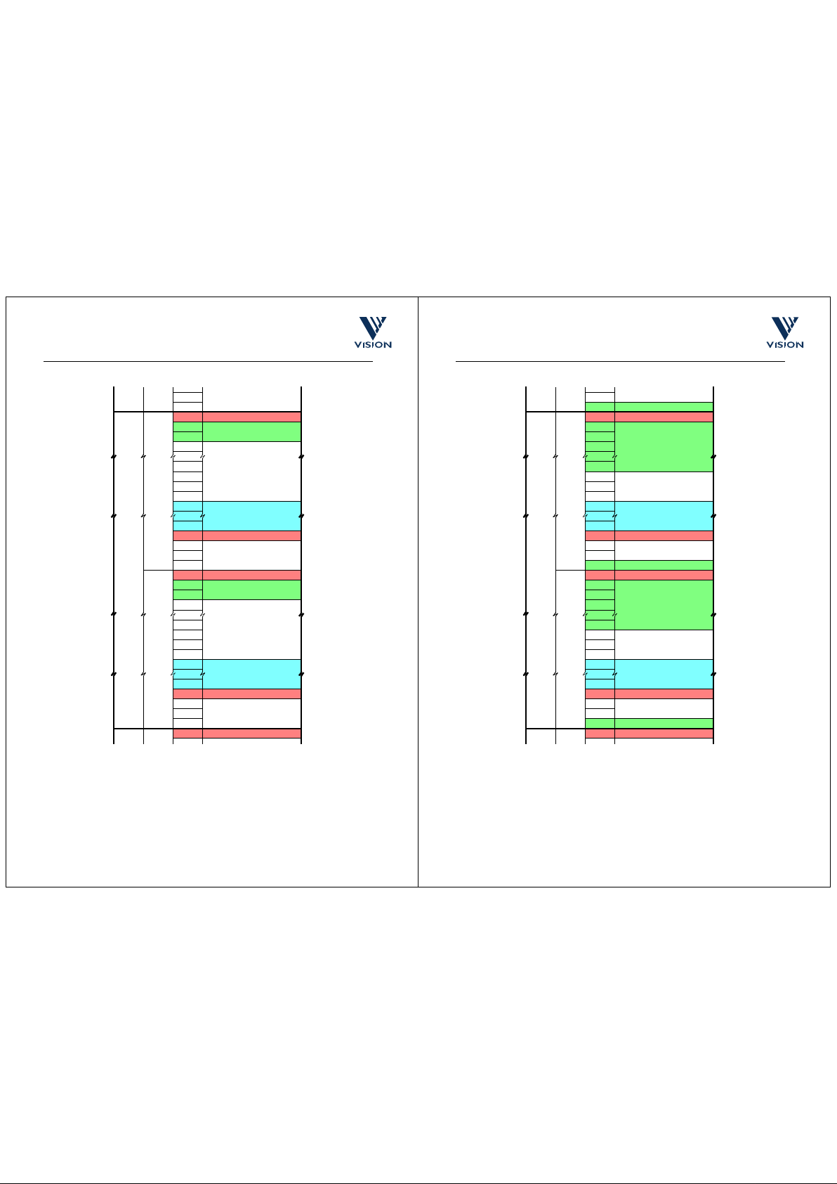
Figure 5.13 : CIF Field and Frame Fo rmats - Borders Off , Extra Bl ack Lin es Off
0
Frame = 608 Lines
Start Of 1st Field Line
2 Black Lines
Start Of 1st Field Line
End Of 1st Field Line
9 Blankin
g
Lines
288 Visible Lines
2nd Field = 304 Lines
1
0
2
3
9
10
11
301
299
300
12
302
303
8
2 Black Lines
Start Of 1st Field Line
End Of 1st Field Line
9 Blanking Lines
288 Visible Lines
1st Field = 304 Lines
1
0
2
3
9
10
11
301
299
300
12
302
303
8
Blanking Lines302
303
3 Blanking Lines
3Blanking Lines
cd38041a.fm 08/10/98 30
VV5409 CMOS Monochrome Sensor Datasheet (Restricted)
Rev 1.0
Commercial In Confidence
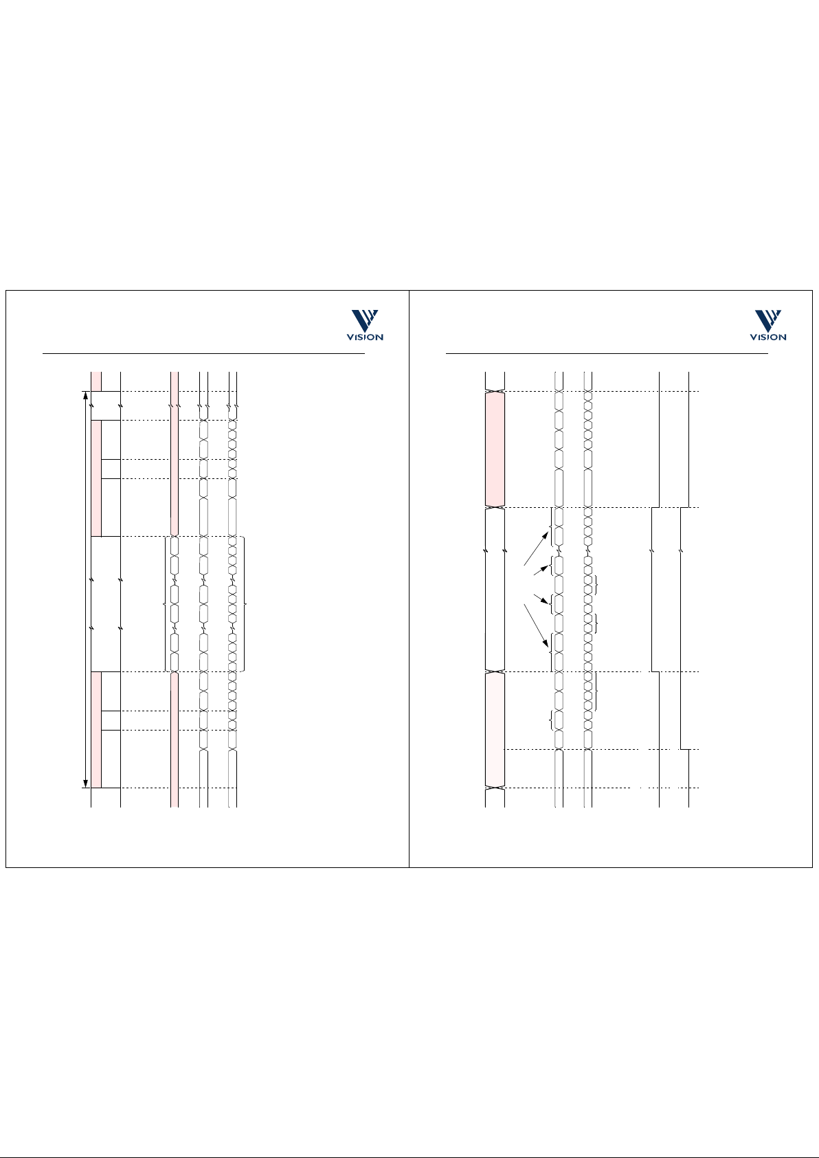
5.3.3 Valid video line timing
All valid video data is contained on active video lines. The pixel data appears as a continuous stream of bytes
Figure 5.14 :
CIF Field and Frame Format
s - Borders Off, Extr a Blac
k Lines On
0
Frame = 608 Lines
Start Of 1st Field Line
8 Black Lines
Start Of 1st Field Line
End Of 1st Field Line
3 Blanking Lines
288 Visible Lines
Black Line
2nd Field = 304 Lines
1
0
2
3
9
10
11
301
299
30012302
30388 Black Lines
Start Of 1st Field Line
End Of 1st Field Line
3 Blanking Lines
288 Visible Lines
Black Line
1st Field = 304 Lines
1
0
2
3
9
1011301
299
30012302
3038Blanking Line
Black Line
302
303
2 Blanking Lines
2 Blanking Lines
Page 16
cd38041a.fm 08/10/98 31
VV5409 CMOS Monochrome Sensor Datasheet (Restricted)
Rev 1.0
Commercial In Confidence
Start of Active Video (SAV)
Line
Figure 5.15 : Line Data Format
End of Active Video (EAV )
Video Data
Y
H
D
1
D
0
D
3
D
2
P
M
P
L
P
M
P
L
P
M
P
L
P
M
P
L
P
M
P
L
P
M
P
L
Number
SAV
8
H
0
H
X
H
Line
Code
Escape/Sync
Sequence
Null
Characters
Line
Code
Escape/Sync
Sequence
P
M
= Pixel Value - Most Significant Nibble, P
L
= Pixel Value - Least Significant Nibble, P = 8-bit Pixel Value
(i)
(ii)
(iii)
(iv)
(v)
Blanking Line (BL)
Black Line (BK)
Visible Line (VL)
Start of Frame (SOF)
End of Frame (EOF)
P = Blanking Level (07
H
)
P = Valid Black Pixel Data
P = Valid Pixel Data
P = Sensor Status Data
P = Blanking Level (07
H
)
N Pixels
0 1 N/2 -1 N/2 N -1 N -2
Pixel Number
4-wire Output Mode
Line Format
8-bit Data
FF
H
00
H
X
H
Y
H
D
3
D
2
D
1
D
0
P P P P P P
FF
H
00
H
80
H
FF
H
0
H
F
H
0
H
F
H
Line Period
F
H
D
1
D
0
D
3
D
2
D
3
D
2
D
1
D
0
cd38041a.fm 08/10/98 32
VV5409 CMOS Monochrome Sensor Datasheet (Restricted)
Rev 1.0
Commercial In Confidence
Start of Active Video
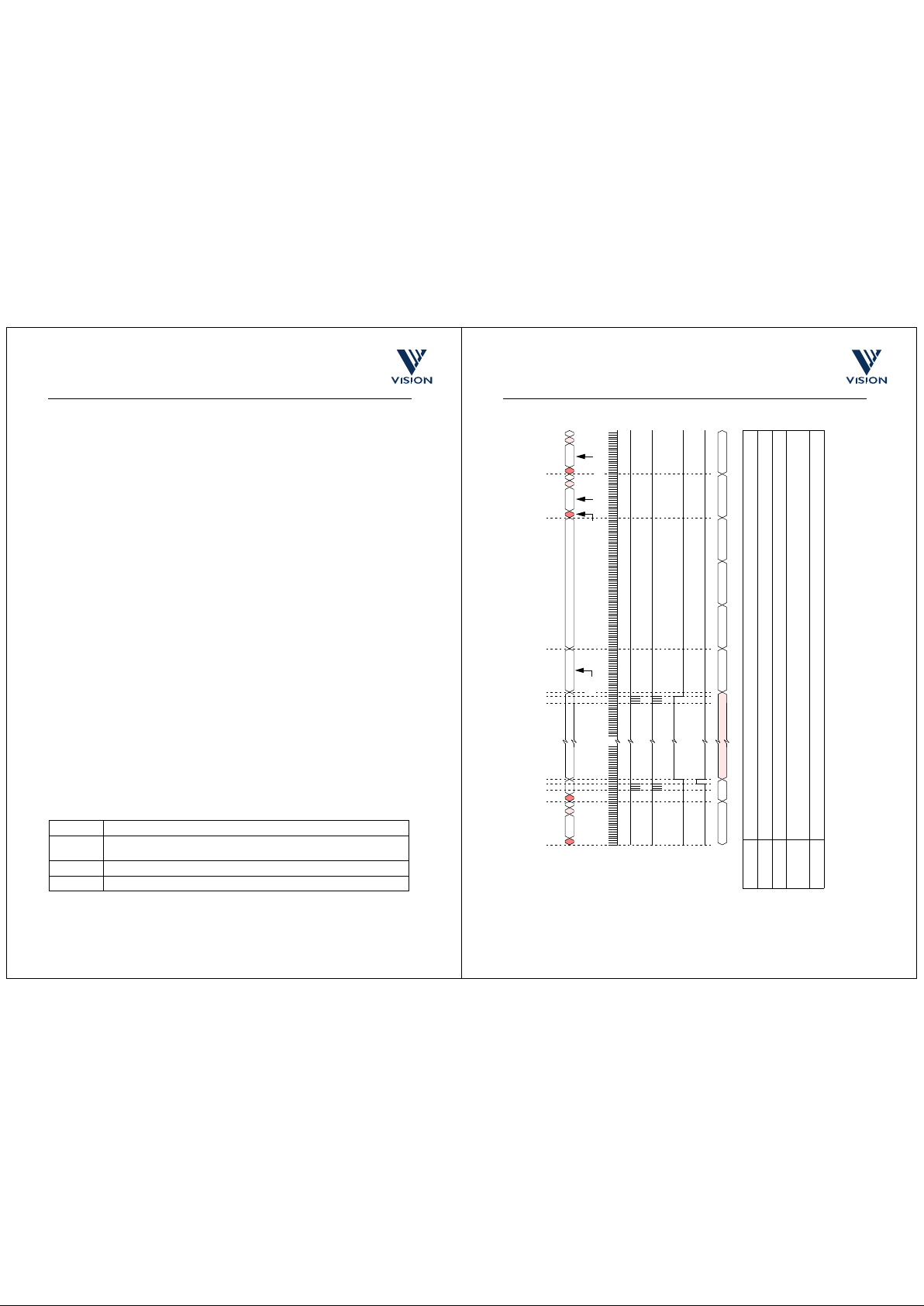
Figure 5.16 : Status Line Data Format and FST/SNO Signals
End of Active Video
Serial Interface Register Values
0
H
1
H
0
H
1
H
0
H
7
H
F
H
F
H
1
H
9
H
(SAV) (EAV)
C
H
7
H
0
H
7
H
0
H
7
H
4
H
0
H
0
H
7
H
0
H
7
H
0
H
7
H
8
H
0
H
0
H
0
H
Start of Frame
Line Code
Line
Number 0
DeviceH
(Register 0)
DeviceL
(Register 1)
Padding
Characters
FF
H
00
H
80
H
FF
H
07
H
07
H
07
H
07
H
19
H
07
H
40
H
07
H
00
H
C7
H
01
H
01
H
FF
H
8-bit Data
4-wire Output Mode
D
1
D
0
D
3
D
2
D
3
D
2
D
1
D
0
F
H
FST Pin:
(ii) Synchronisation Output - SNO
(i) Frame start pulse - qualifies status line information
Page 17
cd38041a.fm 08/10/98 33
VV5409 CMOS Monochrome Sensor Datasheet (Restricted)
Rev 1.0
Commercial In Confidence
within the active lines. The pixel data may be separated from the line header and end-of-line control
sequence by a number of ‘blank’ bytes (07
H
) e.g. when the border lines and pixels are disabled 07H is output
in place of first 2 and last 2 pixels in a valid video line.
5.3.4 Start of frame line timing
The start of frame line which begins each video field contains no video data but instead contains the contents
of all the serial interface registers. This information follows the start-of-line header immediately and is
terminated by an end-of-line control sequence. To ensure that no escape/sync characters appear in the
sensor status/configuration information the code 07
H
is output after each serial interface value. Thus it takes
256 pixel clock periods (512 system clocks) to output all 128 of the serial interface registers. The remainder
of the 356 pixel periods of the video portion of the line is padded out using 07
H
values. The first two pixel
locations are also padded with 07
H
characters (Figure 5.16)
If a serial interface register location is unused then 07
H
is output.
5.3.5 End of frame line timing
The end of frame line which begins each video field contains no video data. Its sole purpose is to indicate the
end of a frame.
5.4 Detection of sensor using data bus state
The video processor device must have internal pull-down terminations on the data bus. On power-up a
sensor will pull all data lines high for a guaranteed period. This scheme allows the presence of a sensor on
the interface to be detected by the video processor on power-up, and the connection of a sensor to an already
power-up interface (a ‘hot’ connection).
The absence of a sensor is detected by the video processor seeing more than 32 consecutive nibbles of 0
H
on the data bus. On detecting the absence of a sensor, CKI, should be disabled (held low).
The presence of a sensor is detected by the video processor seeing more than 32 consecutive nibbles of F
H
on the data bus. On detecting the presence of a sensor, CKI, should be enabled.
5.5 Resetting the Sensor Via the Serial Interface
Bit 2 of setup register 0 allows the VV5409 sensor to be reset to its power-on state via the 2-wire serial
interface. Setting this “Soft Reset” bit causes all of the serial interface registers including the “Soft Reset” bit
to be reset to their default values. This “Soft Reset” leaves the sensor in low-power mode and thus an “Exit
Low-Power Mode” command (Table 6.7, Section 6.6.2) must be issued via the serial interface before the
sensor will start to generate video data (Figure 5.17).
5.6 Power-up, Low-power and Sleep modes
To clarify the state of the interface on power-up and in the case of a ‘hot’ connection of the interface cable
the power-up state of the bus is defined below.
PU0 System Power Up or Sensor Hot Plugged
PU1 Sensor Internal-on Reset Triggers, the sensor enters low power mode and D[3:0] is set
to F
H
.
PU2 Video Processor released from reset.
PU3 Video Processor enables the sensor clock, CLKI.
Table 5.5 : System Power-Up or Hot-plugging Device Behaviour
cd38041a.fm 08/10/98 34
VV5409 CMOS Monochrome Sensor Datasheet (Restricted)
Rev 1.0
Commercial In Confidence
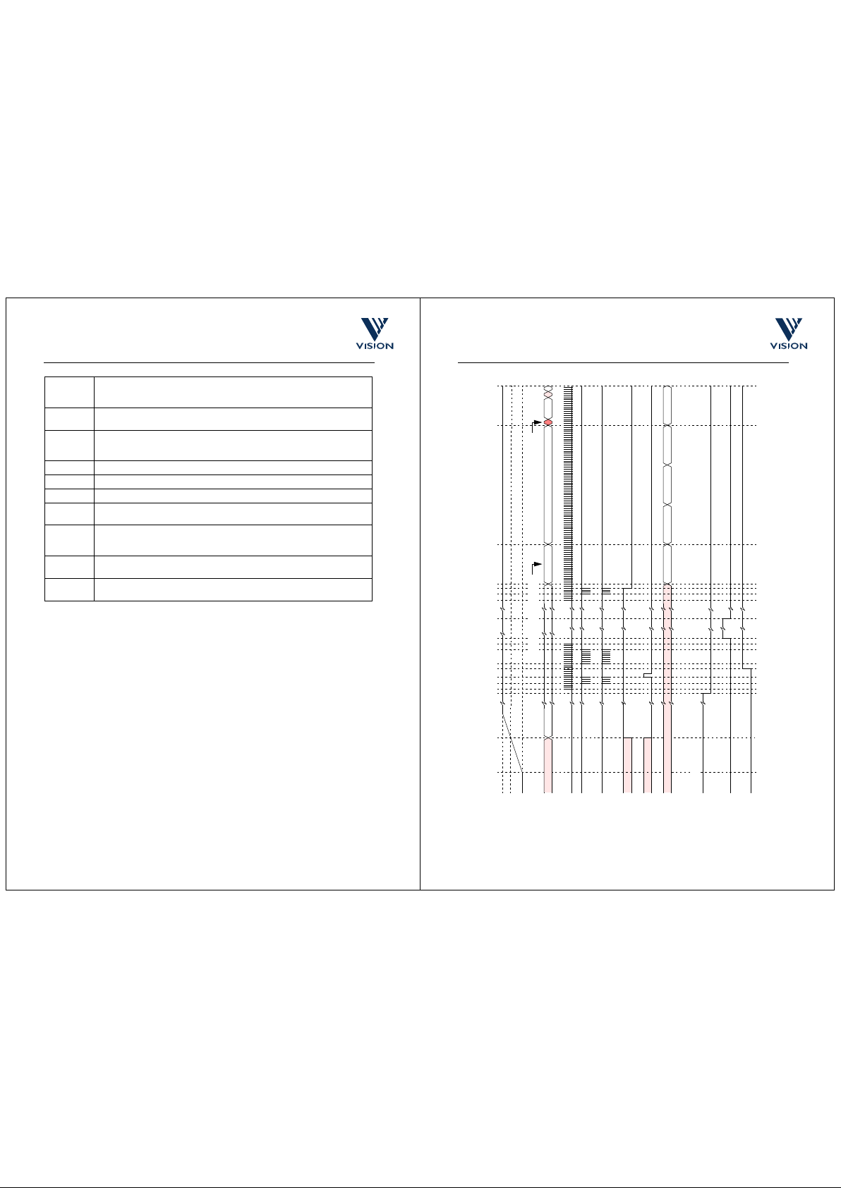
Figure 5.17 : Resetting the VV5409 Sensor via the Serial Interface
F
H
9
H
,6
H
,9
H
,6
H
...
N 0 1
D[3:0]
CLKI
Frame
Number
SDA
SCL
2 3 4 5
Start of Frame Line for the 1st
frame of valid video data.
Valid Video data.
SR0
SR1
SR2
SR6
SR7
setup0[2]
SR0-SR1 “Soft-Reset” Command. At the end of the command the sensor is reset and enters low-power mode.
SR2 The sensor enters low-power mode.
SR3-SR4 “Exit Low Power Mode” Command. Powers-up analogue circuits and initiates the VM5409 sensor’s 4-frame start-up sequence
SR5-SR6 1 Frame of alternating 9
H
& 6
H
data on D[3:0] for the video processor to determine the best sampling phase for the nibble data
(D[3:0]).
SR7-SR8 4 Frames after the “Exit Low-Power mode” command, the sensor starts outputting valid video data.
One frame of 9
H
& 6
H
data.
F
H
SR3
SR4
SR5
SR8
setup0[0]
Page 18
cd38041a.fm 08/10/98 35
VV5409 CMOS Monochrome Sensor Datasheet (Restricted)
Rev 1.0
Commercial In Confidence
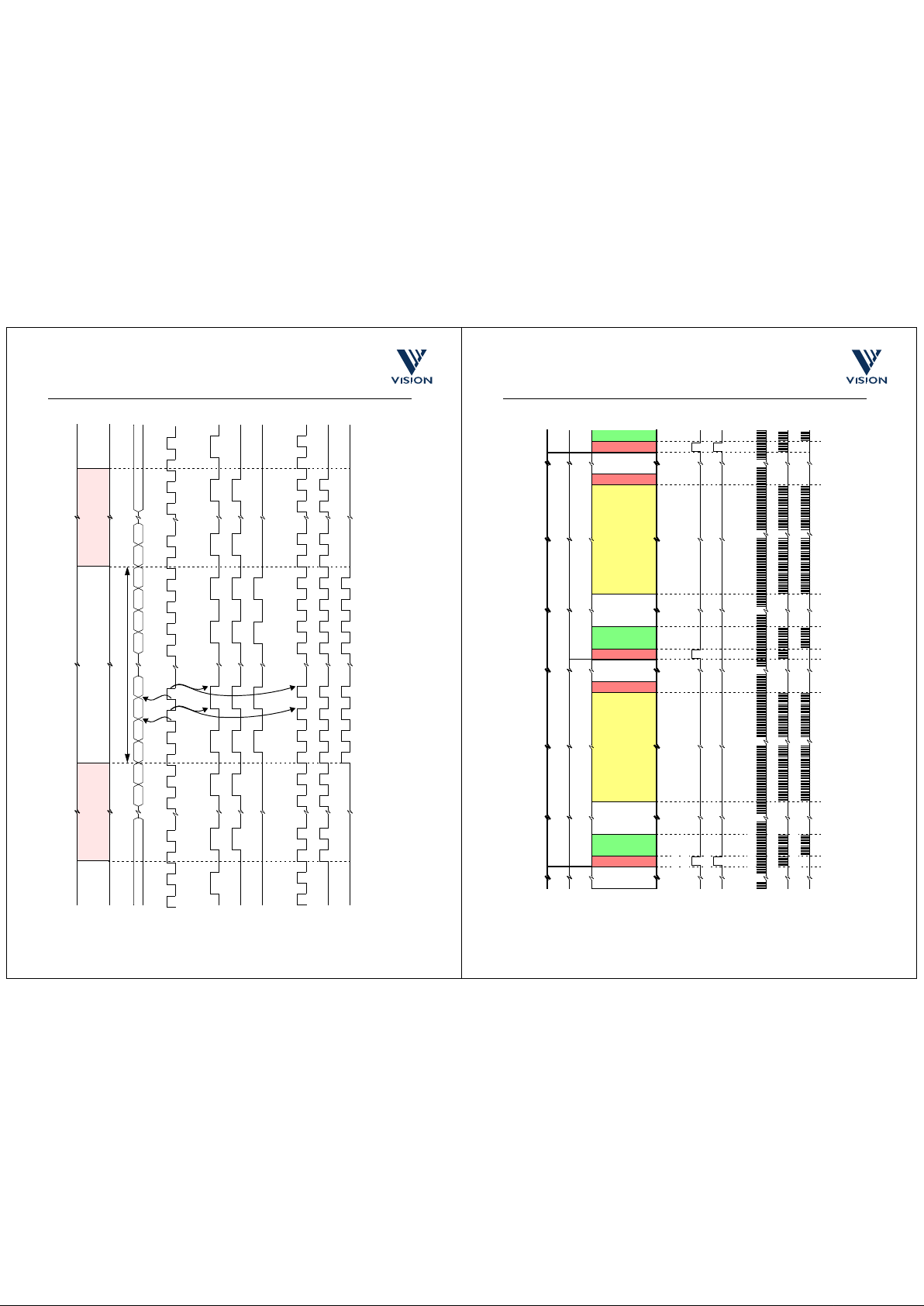
5.6.1 Power-Up/Down (Figure 5.18)
There are two options:
1. Sensor starts running on power-up.
2. Sensor enters low-power after power-up.
The choice of which state the sensor is in on power-up depends of the values of the mode select pins on
power-up
When the sensor starts running on power-up, the power-up sequence is as follows:
1. One field of a continuous stream of alternating 9
H
and 6H values on the data bus. By locking onto the
resulting 0101/1010 patterns appearing on the data bus lines the video processor can determine the
best sampling position for the video data stream.
2. 3 Fields of constant FF
H
(F H) on the data bus
3. 4 Fields after power-up valid video data in generated.
In the case of the sensor entering low-power mode on power-up, the sequence to exit low power-mode is as
follows.
On power-up all of the data bus lines will go high Immediately FF
H
(F H) to indicate that the device is “present”
and the device enters it low-power mode (Section 5.6.2).
When the Video Processor is reset the following sequence should be executed to ensure that the VM5409
starts to generate video data:
1. After the Video Processor has been released from reset, the sensor clock, CLKI, should be enabled
immediately
2. After waiting for at least 16 CLKI clock cycles, a “Soft Reset” command should be issued to the sensor.
This is necessary to ensure that the sensor is brought into a known state. If the sensor is not present
PU4-PU5 At least 16 CLKI clock periods after CLKI has been enabled the host controller must send
a “Soft-Reset” command to the sensor via the serial interface. This ensures that if a
sensor is present then it is in low-power mode.
PU6 On detecting 32 consecutive FF
H
(FH) values on the data bus, the Video Processor sets
the no_camera low.
PU7-PU8 Initiate the Auto-load Daisy-Chain (only where a VISION co-processor is used) to read
setup data and the sensor defect map from the appropriate serial E
2
PROMs into the
sensor and co-processor.
PU9 Video Processor disables the sensor clock, CLKI.
PU10 Video Pr ocesso r generates the VP_Ready interrupt.
PU11 The host software services the VP_Ready interrupt.
PU12 Host issues command to remove sensor from low-power mode. co-processor/hos t
controller enables the sensor clock, CLKI.
PU13-PU4 At least 16 CLKI clock periods after CLKI has been enabled the host controller must send
the “Exit Low-Power Mode” command to the sensor via the serial interface. This initiates
the sensors 4 frame start sequence.
PU15-PU16 One frame of alternating 9
H
& 6H data on D[3:0] for the video processor to determine the
best sampling phase for the nibble data (D[3:0]).
PU17-PU18 4 Frames after the “Exit Low-Power Mode” serial comms, the sensor starts outputting
valid video data.
Table 5.5 : System Power-Up or Hot-plugging Device Behaviour
cd38041a.fm 08/10/98 36
VV5409 CMOS Monochrome Sensor Datasheet (Restricted)
Rev 1.0
Commercial In Confidence
Figure 5.18 : System Power-Up or Hot-plugging Device Behaviour
43
2
10
F
H
F
H
5V
0V
2.8V
9
H
,6
H
,9
H
,6
H
...
Regulated
Sensor
Power
D[3:0]
CLKI
Frame
Number
SDA
SCL
PU0
PU1
PU10
PU3
PU2
PU4
PU5
PU6
PU7
PU8
PU9
PU11
VP dev_reset
PU12
Start of Frame Line for the
1st frame of valid video data.
VP_Ready
Camera_Present
Video Processor
One frame of 9
H
& 6
H
data.
PU13
PU14
PU15
PU16
PU17
PU18
setup0[2]
setup0[0]
Page 19

cd38041a.fm 08/10/98 37
VV5409 CMOS Monochrome Sensor Datasheet (Restricted)
Rev 1.0
Commercial In Confidence
then the serial interface communications by Video Processor will not be acknowledged.
3. Poll for 32 consecutive F
H
values on the data bus, if this condition is satisfied then the sensor is
present. The Video processor should set the camera_present flag.
4. Initiate the Auto-load daisy-chain to read setup data and the defect data from the appropriate serial
CMOS E
2
PROMs into the sensor and co-processor as a appropriate (only where a VISION coo-proc-
essor is used).
5. Disable the sensor clock CKI.
6. The Video Processor should generate the VP_Ready interrupt.
7. Once the host software serviced the VP_Ready interrupt, then the sensor and video processor is ready
to generate video data.
8. To enab le video data, the host software, sets the low-power mode bit low. The video processor must
enable CLKI at least 16 CLKI clock cycles before issuing the “Exit Low-Power Mode” command via the
serial interface.
After the “Exit Low-Power Mode” command has been sent the sensor will output for one frame, a continuous
stream of alternating 9
H
and 6 H values on D[3:0]. By locking onto the resulting 0101/1010 patterns
appearing on the data bus lines the video processor can determine the best sampling position for the nibble
data. After the last 9
H
6 H pair has been output the data bus returns to F H until the start of fifth frame after
CKI has been enabled when the first active frame output. After the video processor has determined the
correct sampling position for the data, it should then wait for the next start of frame line (SOF).
If the video processor detects 32 consecutive 0
H
values on the data bus, then the sensor has been removed.
The sensor clock, CKI, should be held low.
5.6.2 Low-Power Mode
Under the control of the serial-interface, the sensor’s analogue circuitry can be powered-down, and then
powered-up. When the low-power bit is set through the serial-interface, all the data-bus lines will go high at
the end of the current frame’s, end-of-frame line. At this point the analogue circuits in the sensor, will powerdown. The system clock must remain active for the duration of low power mode.
Only the analogue circuits are powered-down, the values of the serial-interface registers e.g. exposure, and
gain are preserved.
The internal frame timing is reset to the start of a video frame, on exiting low-power mode.
In a similar manner to the previous section, the first frame after the serial comms contains a continuous
stream of alternating 9
H
and 6 H to allow the video processor to re-confirm its sampling position. Then three
frames later the first start-of-frame line is generated.
5.6.3 Sleep Mode
Sleep mode is similar to the low-power mode, except that the analogue circuitry remains powered. When the
sleep command is received through the serial-interface, the pixel-array will be put into reset, and all the datalines will go high at the end of the current frame. Again the system clock must remain active for the duration
of the sleep mode.
When the sleep mode is disabled, the CMOS sensor’s frame timing, is reset to the start of a frame. During
the first frame, after exiting from the sleep mode, the data-bus will remain high, while the exposure value
propagates through the pixel-array. At the start of the second frame, the first start-of-field line will be
generated.
5.6.4 Application of the system clock during sensor low-power modes
For successfully entry and exit into and out of low power and ‘sleep’ modes the system clock, CLKI, must
remain active for the duration of these modes.
cd38041a.fm 08/10/98 38
VV5409 CMOS Monochrome Sensor Datasheet (Restricted)
Rev 1.0
Commercial In Confidence
5.7 Qualification of Output Data
There are two distinct ways for qualifying the data nibbles appearing of the output data bus
5.7.1 Using the External Clock signal applied to CLKI
The data on the output data bus, changes on the rising edge of CLKI. The delay between the video processor
supplying a rising clock edge and the data on the data bus becoming valid, depends on the length of the cable
between the sensor and the video processor. To allow the video processor to find the best sampling position
for the data nibbles, via the serial interface the data bus can be forced to output continuously 9
H
, 6H, 9H, 6H,...
5.7.2 Data Qualification Clock, QCK
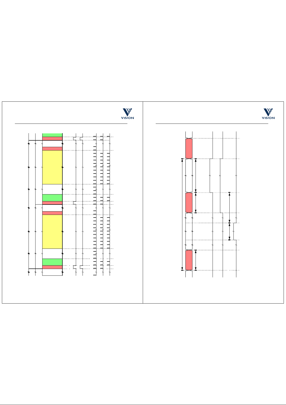
VV5409 provides a data qualification clock for the output bus There are two frequencies for the qualification
clock: one runs at the nibble rate and the other at the pixel read-out rate. The falling edge of the fast QCK
qualifies every nibble irrespective of whether it is most or least significant nibble. For the slow QCK, the rising
edge qualifies the most significant nibbles in the output data stream and the falling edge qualifies the least
significant nibbles in the output data stream.
There are 4 modes of operation of QCK.
1. Disabled (Always low - (Default)
2. Free running - qualifies the whole of the output data stream.
3. Embedded control sequences, status data and pixel data.
4. Pixel Data Only.
The operating mode for QCK is set via the serial interface. The QCK output is tri-stated when OEB is high.In
one of the modes available via the serial interface the slow version of QCK will appear on the QCK pin while
the fast version of the same signal will appear on the FST pin.
In the case where the border rows and columns are disabled, there is simply no qualification pulse at that
point in time i.e. when pixels 0,1, 354 and 355 are normally output.
The QCK pin can also be configured to output the state of a serial interface register bit. This feature allows
the sensor to control external devices, e.g. stepper motors, shutter mechanisms. The configuration details
for QCK can be found in sections 5.5.7 and 5.5.8 of this document.
5.7.3 Line Start Signal, LST
There are 4 modes of operation for the LST pin programmable via the serial interface:
1. Disabled (Always Low- Default).
2. Free running - LST signal occurs once at the beginning of every line.
3. All lines except blanking lines are qualified by LST.
4. Only Black and Visible Lines are qualified by LST.
The LST is tri-stated when OEB is high.
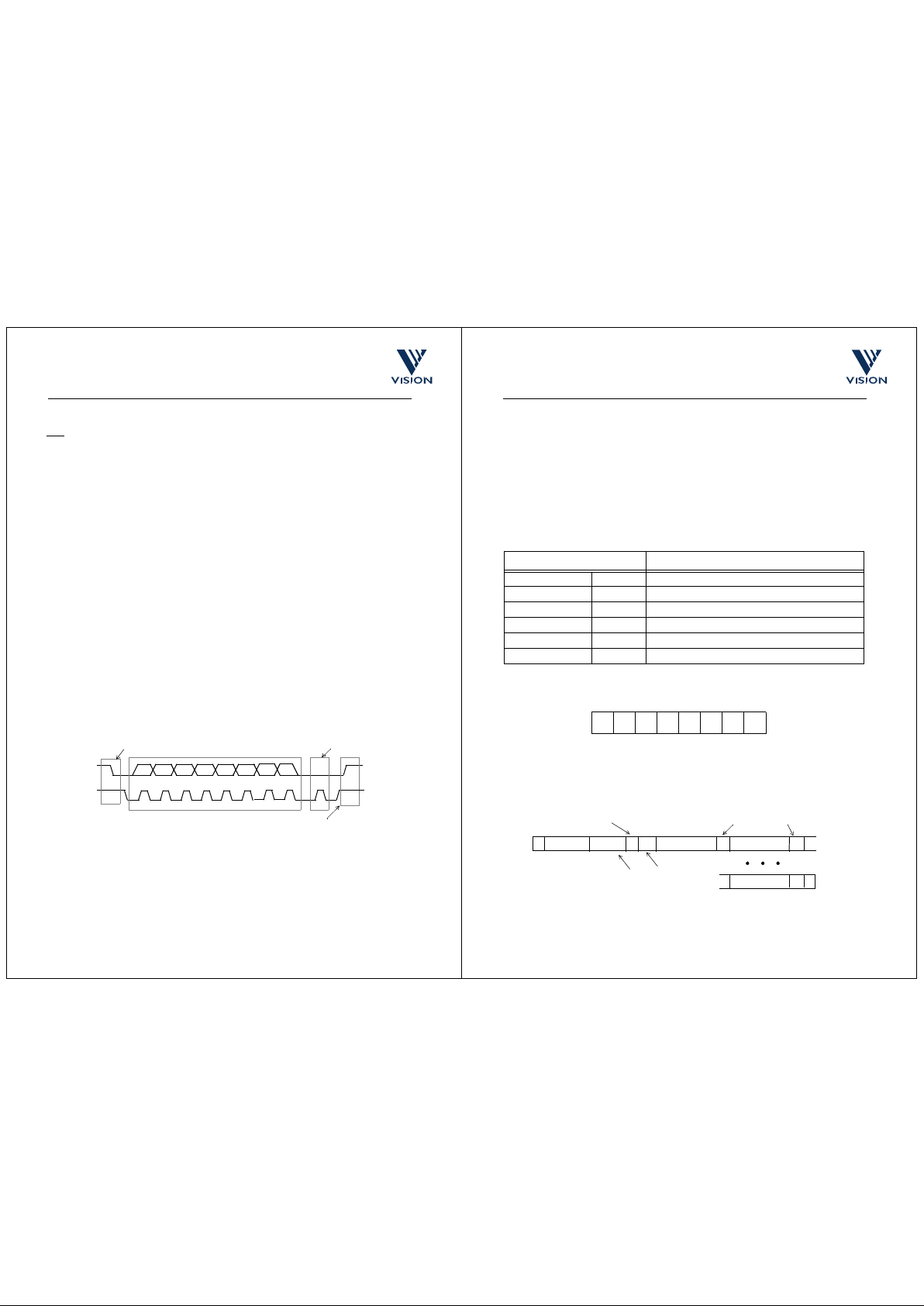
5.7.4 Frame Start Signal, FST
There are 3 modes of operation for the FST pin programmable via the serial interface:
1. Disabled (Always Low- Default).
2. Frame start signal. The FST signal occurs once frame, is high for 356 pixel periods (712 system clock
periods) and qualifies the data in the start of frame line.
3. Synchronisation Output Pulse -SNO - Refer to Section 8. on Synchronising multiple cameras.
4. As the de-bounced switch input.
Note
: The function of the SNO pin has not been verified.
The FST is tri-stated when OEB is high.
The FST pin can also be configured to output the state of a serial interface register bit. This feature allows
Page 20
cd38041a.fm 08/10/98 39
VV5409 CMOS Monochrome Sensor Datasheet (Restricted)
Rev 1.0
Commercial In Confidence
End of Active V i deo
(EAV)
Start of Active Video
(SAV)
Pixel Data
Figure 5.19 : Qualification of Output Data (Border Rows and Columns Enabled)
Video Data
F
H
Line Format
4-wire Nibble Output Mo de - D[3 :0 ]
D
1
D
0
F
H
F
H
F
H
P
M
P
L
P
M
P
L
P
M
P
L
P
M
P
L
External clock applied to CLKI
Slow Qualification Clock, QCK
(i) Free running
(ii) Control sequences and Pixel Data
(iii) Pixel Data only
P
M
= Pixel Value - Most Significant Nibble, P
L
= Pixel Value - Least Significant Nibble, P = 8-bit Pixel Value
Fast Qualification Clock, QCK
(i) Free running
(ii) Control sequences and Pixel Data
(iii) Pixel Data only
cd38041a.fm 08/10/98 40
VV5409 CMOS Monochrome Sensor Datasheet (Restricted)
Rev 1.0
Commercial In Confidence
the sensor to control external devices, e.g. stepper motors, shutter mechanisms.
Figure 5.20 : Frame/Field Level Timings for FST and QCK
Start of Field
Black Lines
Blanking Lines
Visible Lines
End of Field
Blanking Lines
Blanking Lines
Start of Field
2nd Field
1 Frame
Start of Field
Black Lines
Blanking Lines
Visible Lines
End of Field
Blanking Lines
1st Field
Frame/Field Format:
QCK:
(iii) Data Only
(ii) Control plus Data
(i) Free Running
(ii) SNO
FST Pin:
(i) FST
Page 21
cd38041a.fm 08/10/98 41
VV5409 CMOS Monochrome Sensor Datasheet (Restricted)
Rev 1.0
Commercial In Confidence
The configuration details for FST can be found in Section 6.6.2 of this document.
Figure 5.21 : Frame/Field Level Timings for FST and LST
Start of Field
Black Lines
Blanking Lines
Visible Lines
End of Field
Blanking Lines
Blankin
g
Lines
Start of Field
2nd Field
1 Frame
Start of Field
Black Lines
Blanking Lines
Visible Lines
End of Field
1st Field
Frame/Field Format:
LST:
(iii) Data Only
(ii) Control plus Data
(i) Free Running
(ii) SNO
FST Pin:
(i) FST
Blanking Lines
cd38041a.fm 08/10/98 42
VV5409 CMOS Monochrome Sensor Datasheet (Restricted)
Rev 1.0
Commercial In Confidence
Figure 5.22 : Line Level Timings for FST and LST
Video
Data
Start of Active
Video (SAV)
Video Data - 306/356 Pixels
EAV
Inter-line Period (Data Bus = F
H
)
End of Active
Video (EAV)
FST Pin:
(ii) Synchronisation Output - SNO
(i) Frame start pulse - qualifies status line information
End of Active
Video (EAV)
LST Pin:
6 Pixels 306/356 Pixels6 Pixels
1 Line
LST width LST (f) to Start of Video
Page 22
cd38041a.fm 08/10/98 43
VV5409 CMOS Monochrome Sensor Datasheet (Restricted)
Rev 1.0
Commercial In Confidence
6. Serial Control Bus
Note
: Where ‘Recommended settings’ are given in Section 6.5 and Section 6.6, it is recommended that these
settings are writen to the camera registers on startup, for correct operation of the sensor. This applies to the
Setup0 [16], Setup1 [17], and at1 [121] registers in particular.
6.1 General Description
Writing configuration information to the video sensor, and reading both sensor status, and configuration
information, back from the sensor, is performed through the 2-wire serial-interface.
Communication using the serial-control-bus, centres around a number of registers internal to the video
sensor. These registers, store the sensor status, set-up, exposure, and system information. Most of the
registers are read/write, allowing the receiving equipment to change their contents. Others (such as the chip
ID) are read only.
The main features of the serial-interface include:
• Sensor address is now fixed at 20
H
/21 H (whereas in VV6407, 2 possible sensor addresses could be
set by means of the SA[0] pin)
• Broadcast address, to ease setting up multiple camera configurations
• Variable length read/write messages
• Indexed addressing of information source, or destination within the sensor
• Automatic update of the index, after a read, or write message
• Message abort, with negative acknowledge, from the master
• Byte oriented messages.
The contents of all internal registers, accessible through the serial-control-bus, are encapsulated in each
start-of-field line - see Section 5.3.4.
6.2 Serial Communication Protocol
The host controller must perform the role of a communications master, while the camera acts as either a
slave receiver, or transmitter.The communication from host to camera, takes the form of 8-bit data, with a
maximum serial clock video processor frequency of 100 kHz. Since the serial clock is generated by the busmaster, it determines the data transfer rate. Data transfer protocol on the bus is shown below.
6.3 Data Format
Information is packed in 8-bit packets (bytes) always followed by an acknowledge bit. The internal data is
produced by sampling
SDA,
at a rising edge of
SCL
. The external data must be stable during the high period
of
SCL
. The exc e pt i ons to th i s a r e
start
(S) or
stop
(P) conditions when
SDA
falls, or rises resp ective ly, whi le
12
7
8
A
Start condition
Stop condition
SDA
SCL
Acknowledge
P
S
3 4 56
Address or data byte
MSB LSB
Figure 6.1 : Serial-Interface Data Transfer Protocol
cd38041a.fm 08/10/98 44
VV5409 CMOS Monochrome Sensor Datasheet (Restricted)
Rev 1.0
Commercial In Confidence
SCL
is high.
A message contains at least two bytes, preceded by a
start
condition, and followed by either a
stop,
or
repeated start, (Sr)
followed by another message.
The first byte contains the device address byte, which includes the data direction
read,
(r)
, ~write
, (~w), bit.
The allocation of serial-interface addresses for sensors, VISION co-processors, and serial E
2
PROMs is
defined in Table 6.1.The lsb of the address byte, indicates the direction of the message. If the lsb is set high,
the master will read data from the slave, and if the lsb is reset low, the master will write data to the slave. After
the
r, ~w
bit is sampled, the data direction cannot be changed until the next address byte, with a new
r, ~w
bit is received.
In addition to its own specific address, the VV5409 also responds to the sensor and VISION co-processor;
and sensor only, serial-interface addresses. These additional addresses allow sensors and/or VISION coprocessors to be written to in parallel, through the serial-interface bus. The broadcast addresses are only
intended for writing, not reading.
The byte following the address byte contains the address of the first data byte (also referred to as the
index
).
The serial-interface, can address up to 128 registers. If the msb of the second byte is set, the automatic
increment feature of the address index, is selected.
Serial Address Comment
1010_XXX_R/W A0H - AFHSerial E2PROM - 8 possible addresses
0010_000_R/W 20
H
- 21HSensor - address (fixed).
0010_1XX_R/W 28
H
- 2FHVISION Co-processor - 4 possible addresses
0011_000_R/W 30
H
& 31HSensor and VISION Co-processor Broadcast Address
0011_001_R/W 32
H
& 33HSensor Only Broadcast Address
0011_010_R/W 34
H
& 35HVISION Co-processor Only Broadcast Address
Table 6.1 : Allocation of Serial-Interface Addresses
0 0 1 0 0 0 0
Figure 6.2 :
VV
5409
Serial Interface Address
R/W
S
address[7:1]
R
/
W
bitADATA[7:0]
A
Sensor acknowledges valid address
Acknowledge from slave
INDEX[6:0]
INC
P
A
A
DATA[7:0]
[0]
address
Auto increment
Index bit
Figure 6.3 :
Serial-Interface Data Format
Page 23
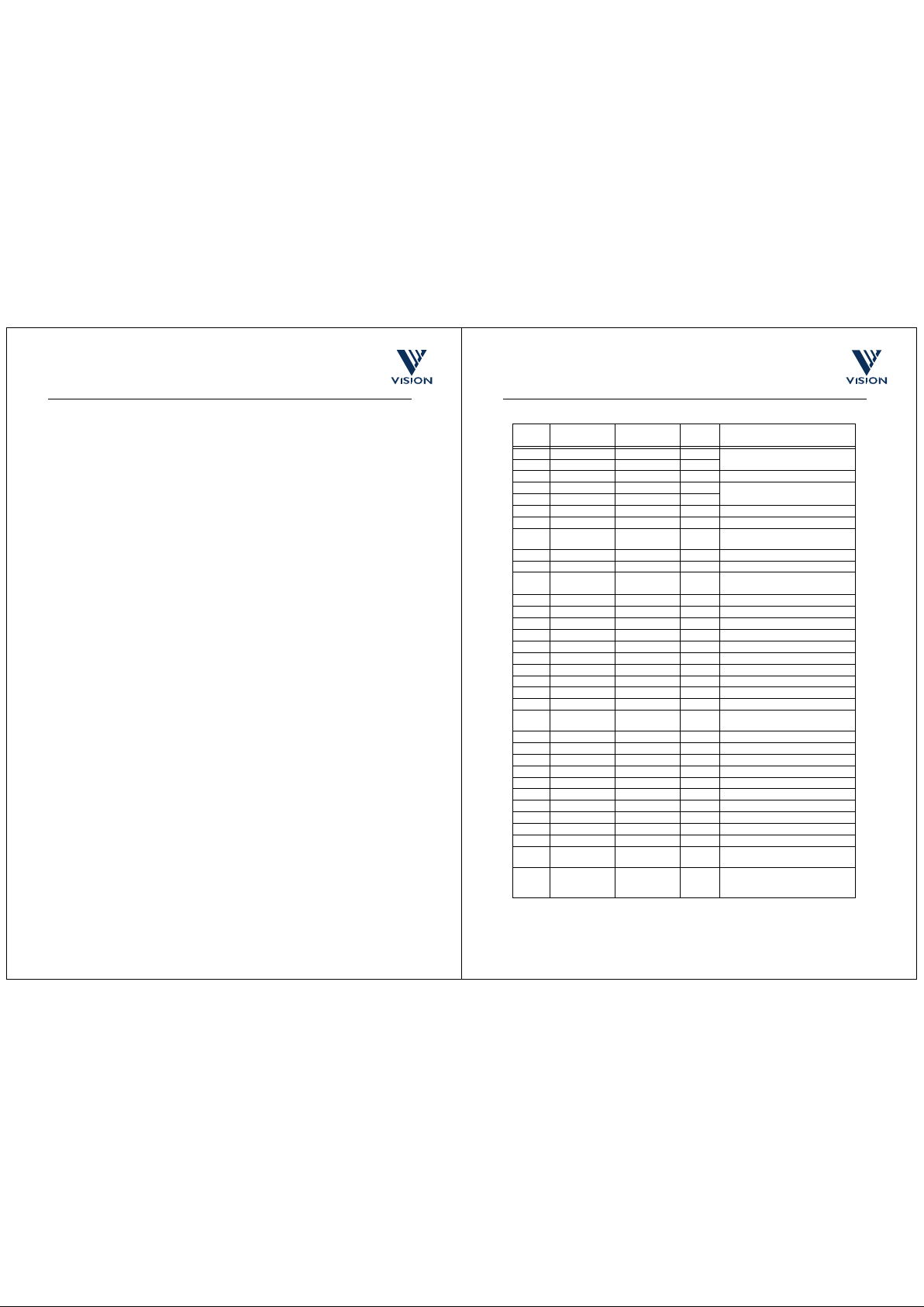
cd38041a.fm 08/10/98 45
VV5409 CMOS Monochrome Sensor Datasheet (Restricted)
Rev 1.0
Commercial In Confidence
6.4 Message Interpretation
All serial-interface communications with the sensor, must begin with a
start
condition. If the
start
condition is
followed by a valid address byte, further communications can take place. The sensor will acknowledge the
receipt of a valid address, by driving the
SDA
wire low. The state of the
read/~write
bit (lsb of the address
byte) is stored, and the next byte of data, sampled from
SDA,
can be interpreted.
During a write sequence, the second byte received is an address index, which points to one of the internal
registers. The msbit of the following byte, is the
index auto increment
flag. If this flag is set, then the serialinterface will automatically increment the index address, by one location, after each slave acknowledge. The
master can therefore send data bytes continuously to the slave, until either:
1. The slave fails to provide an acknowledge
2. The master terminates the write communication with a
stop
condition
3. The master sends a
repeated start, (Sr)
.
If the auto increment feature is used, the master does
not
have to send indexes to accompany the data bytes.
As data is received by the slave, it is written bit by bit to a serial/parallel register. After each data byte has
been received by the slave, an acknowledge is generated. The data is then stored in the internal register,
addressed by the current index.
During a read message, the current index is read out from the byte following the device address byte. The
next byte read from the slave device, is the contents of the register addressed by the current index. The
contents of this register, is then parallel loaded into the serial/parallel register, and clocked out of the device
by
SCL.
At the end of each byte, in both read and write message sequences, an acknowledge is issued by the
receiving device. Although VV5409 is always considered to be a slave device, it acts as a transmitter when
the bus-master requests a read from the sensor.
At the end of a sequence of incremental reads or writes, the terminal index value in the register will be one
greater
than the last location read from, or written to. A subsequent read will use this index to begin retrieving
data from the internal registers.
A message can only be terminated by the bus master, either by issuing a stop condition, a repeated start
condition, or by a negative acknowledge, after reading a complete byte during a read operation.
6.5 The Programmers Model
The serial interface programmer’s model allows for up to 128, 8-bit registers within the sensor, accessible by
the user through the serial-interface. They are grouped, according to function, with each group occupying a
16-byte page of the location address space. There may be up to eight such groups, although this scheme is
purely a conceptual feature, and not related to the actual hardware implementation, The primary categories
are given below:
• Status Registers (Read Only)
• Setup registers, with bit significant functions
• Exposure parameters, which influence output image brightness
• System functions, and analogue test bit significant registers.
Any internal register which can be written to, can also be read from. There are several read-only registers,
which contain device status information, (e.g. design revision details).
Names which end with H or L, denote the most, or least-significant, part of the internal register. Note that
unused locations in the H byte, are packed with zeroes.
VISION sensors, which include a 2-wire serial-interface, are designed with a common address space. If a
register parameter is unused in a design, but has been allocated an address in the generic design model, the
location is referred to as
reserved
. If the user attempts to read from any of these
reserved, or unused
locations, a default byte will be read back. In VV5409 this data is 07H. A write instruction to a reserved (but
unused) location is illegal, and will not be successful, as the device will not allocate an internal register to the
data-word contained in the instruction.
cd38041a.fm 08/10/98 46
VV5409 CMOS Monochrome Sensor Datasheet (Restricted)
Rev 1.0
Commercial In Confidence
A detailed description of each register follows.
Index Name
Recommended
Setting
Register
Type
Comments
0 deviceH RO Chip identification number including
revision indicator
1 deviceL RO
2status0 RO
3 line_countH RO Current line counter value
4 line_countL RO
5 - 11 reserved
12-15 unused
16 setup0 1000_x000
2
R/W Low-power/sleep modes & Video
Timing
17 setup1 01x0_0010
2
R/W Black Calibration
18-19 reserved R/W reserved
20 fg_modes R/W Frame grabbing modes
(FST, LST and QCK)
21 pin_m apping R/ W FST and QCK mapping modes
22 unuse d unused
23 op_format R/W Output coding format
24-31 unused unused
32 fineH R/W Fine exposure
33 fineL R/W Fine exposure
34 coarseH R/W Coarse exposure
35 coarseL R/W Coarse exposure
36 gain R/W ADC Pre-amp gain setting
37 clk_div R/W Clock division
38-111 unused/
reserved
unused/reserved
112 bcal_win R/W Black Calibration Window Select
113 bcal0 R/W Black calibration DAC0
114 bcal1 R/W Black calibration DAC1
115 reserved
116 tms0 R/W Reserved
117 cr0 R/W Analogue Control Register 0
118 cr1 R/W Analogue Control Register 1
119 as0 R /W ADC Setup Register
120 at0 R/W Analogue Test Register
121 at1 0F
H
R/W Microphone Amp Setup Register
122-
126
unused/
reserved
unused/reserved
127 reserved Defect SRAM Auto-load Address,
where required. Contact VLSI VISION
for details
Table 6.2 : VV5409 Serial-Interface Address Map.
Page 24
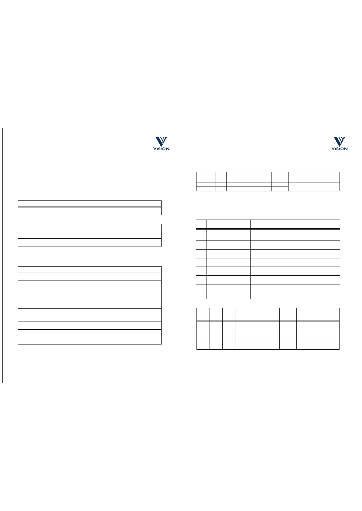
cd38041a.fm 08/10/98 47
VV5409 CMOS Monochrome Sensor Datasheet (Restricted)
Rev 1.0
Commercial In Confidence
6.6 Register descriptions
6.6.1 Status Registers - [0 - 15]
[0-1] - DeviceH and DeviceL
These registers provide read-only information, which identifies the sensor type, coded as a 12-bit number,
and a 4-bit mask set revision identifier. The device identification number, for VV5409 is 409 i.e. 0001 1001
0111
2
.
The initial mask revision identifier is 0 i.e. 0000
2
.
[2] - Status0
Bits Function Default Comment
7:0 Device type identifier 0001 10012Most significant 8 bits of the 12 bit code identifying
the chip type
Table 6.3 : [0] - DeviceH
Bits Function Default Comment
7:4 Device type identifier 01112Least significant 4 bits of the 12 bit code identifying
the chip type
3:0 Mask set revision identifier 1010
2 or
1101
2
Table 6.4 : [1] - DeviceL
Bit Function Default Comment
0 Exposure v alue update pending 0 Exposure sent, but not yet consumed by the
exposure controller
1 Gain value update pending 0 Gain value sent, but not yet consumed by the
exposure controller
2 C lock divisor update pend ing 0 Clock divisor sent, but not yet consumed by the
exposure controller
3 Black calibration fail flag 0 If the black calibration has failed, this flag will be
raised. It will stay act iv e until the last line of the
next
successful
black calibration
4 Odd/ even frame 1 The flag, will toggle-state on alternate frames
5 Video Timing upd ate pend ing 0 New line, or frame length, value written, but not
yet consumed by the video timing controller
6 Debounced Digital Input Flag 0 Debounced, and re-timed version, of DIN pin. If
set, cleared at end of status line
7 Auto-loa d Succes sful 0 S et if auto-load has been com pleted
successfully, (where used) i.e. E
2
PROM present
and no serial communications errors have
occurred.
Table 6.5 : [2] - Status0
cd38041a.fm 08/10/98 48
VV5409 CMOS Monochrome Sensor Datasheet (Restricted)
Rev 1.0
Commercial In Confidence
[3-4] - Line_countH & Line_countL
6.6.2 Setup Registers - [16 - 31]
[16] - Setup0
Register
Index
Bits Function Default Comment
3 0:0 Current line count MSB - Displays current line count
4 7:0 Current line count LSB -
Table 6.6 : Current Line Counter Value.
Bit Function
Recommended
setting
Comment
0 Low Power Mode:
Off /
On
0
(Default 1)
Powers down the sensor-array. The output
data-bus goes to F
H
. On power-up, the sensor
enters low power mode
1 Sleep Mod e:
Off
/ On
0 Puts the sensor-array into reset. The output
data-bus goes to F
H
2 Soft Reset
Off
/ On
0 Setting this bit, resets the sensor to its power-
up defaults. This bit is also reset
3 Frame/Field Rate select:
25 fps (PAL) /
30 fps (NTSC)
1 (NTSC)
0 (PA L)
Frame/Field Rate select
4 Tri-state output data-bus
Outputs Enabled
/ Tri-state
0 On power-up, the data-bus pads are enabled
by default
5 Re-time tri-state update.
Off
/ On
0 Re-time, new tri-state value to a field boundary
7:6 Video Timing Mode Select As required
(Defult 00)
00 - CIF Timin
g
Modes
01 - PAL/ NTSC 13.5 MHz Timing Modes
10 - PAL/NTSC 3.2 fsc Timing Modes
11 - unused.
Table 6.7 : Setup0 [16]
Video
Mode
setup0
bits
[7:6]
setup0
bit [3]
Pixel
Clock
Divisor
Video
Data
Line
Length
Field
Length
Data
Format
Comment
000
2
0 2 356 x 292 471 304 4-wire CIF - 25 fps
1 1 2 356 x 292 393 304 4-wire CIF - 30 fps
201
2
0 2 356 x 292 432 312/313 4-wire PAL(13.5 MHz)
3 1 2 306 x 244 429 262/263 4-wire NTSC
(13.5 MHz)
Table 6.8 : Video Timing Modes
Page 25
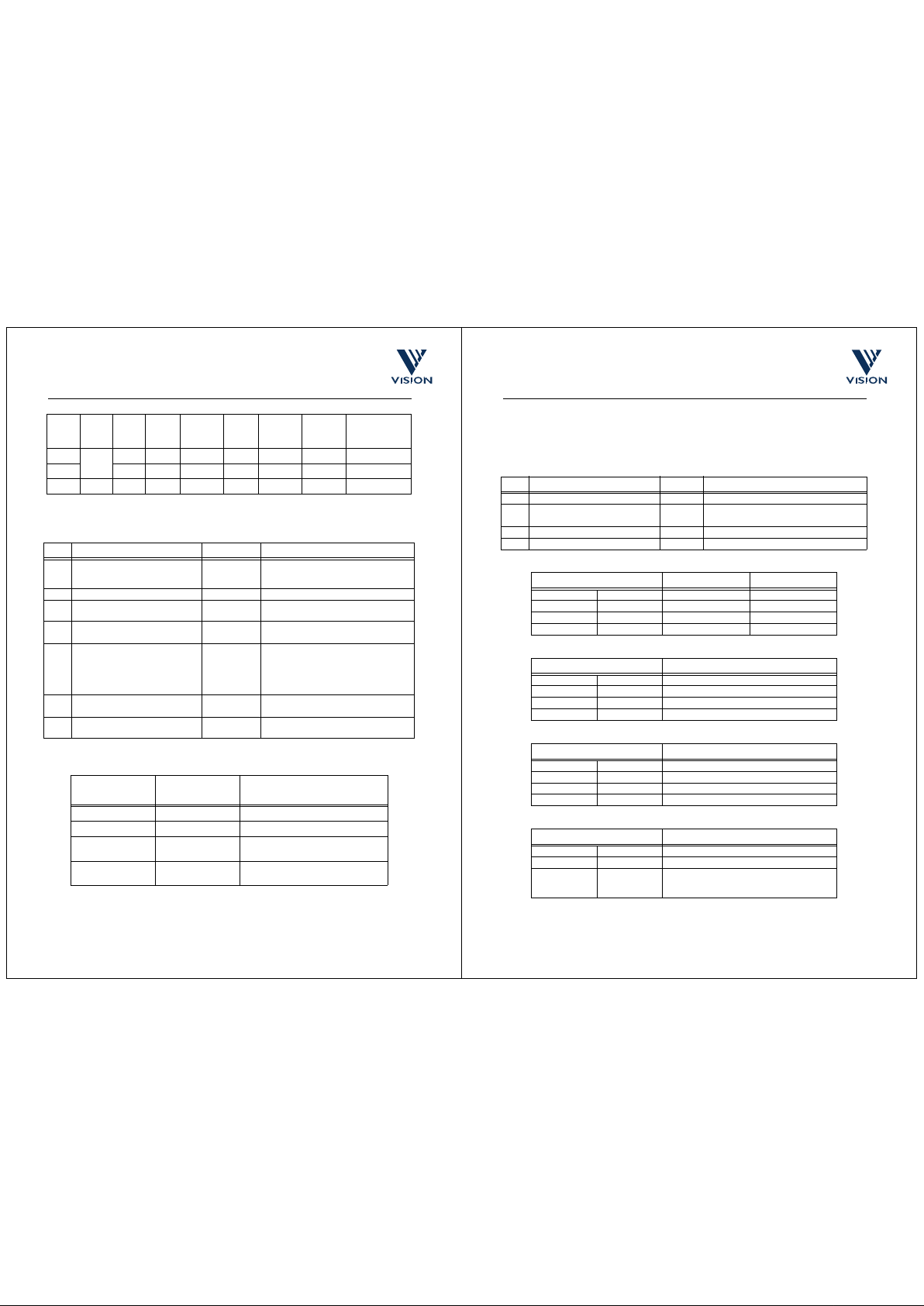
cd38041a.fm 08/10/98 49
VV5409 CMOS Monochrome Sensor Datasheet (Restricted)
Rev 1.0
Commercial In Confidence
[17] - Setup1
If the gain, change trigger option, has been selected, then care should be taken when writing the new gain
410
2
0 2 356 x 292 454 312/313 4-wire PAL (3.2 fsc)
5 1 2 306 x 244 364 262/263 4-wire NTSC (3.2 fsc)
6-7 11
2
X Unused
Bit Function Default Comment
1:0 Black calibration mode selection 10 Black calibration trigger selection. Default
setting decision based on result of monitor
test. See table below
2 reserved
3 Enable immediate clock division
update.
Off
/On
0 Allow manual change, to clock-division, to
be applied immediately
4 Enable immediate gain update.
Off
/On
0 Allow manual change, to gain, to be
applied immediately
5 Enable additional black lines (lines
3-8)
Off
/On
0 If enabled, this bit, will enable the lines
immediately following the end-of-frame
line
0 - CIF
1 - NTSC and PAL (13.5 MHz and 3.2 fsc)
6 Border rows and columns:
Masked or
Output
1 These extra pixels/rows are optional
7 Res erved 1 Must be set to 0 for normal pixel readout
(see Section 2.2)
Table 6.9 : [17] - Setup1
Black Calibration
Mode[1]
Black Calibration
Mode[0]
Comment
0 0 No black calibration
01
Always
trigger black calibration
1 0 Black calibration triggered by a
failed
monitor test
1 1 Trigger black calibration only if the gain
setting changes
Table 6.10 : Black Calibration Mode
Video
Mode
setup0
bits
[7:6]
setup0
bit [3]
Pixel
Clock
Divisor
Video
Data
Line
Length
Field
Length
Data
Format
Comment
Table 6.8 : Video Timing Modes
cd38041a.fm 08/10/98 50
VV5409 CMOS Monochrome Sensor Datasheet (Restricted)
Rev 1.0
Commercial In Confidence
value if the
immedi at e ga i n u p da te
option has been selected. It is strongly advised that the user should
not
write a new gain value between line 0 (the status line) and line 9 (the last black calibration line). If the gain
values are written in a timed manner, then no restriction applies.
[20] - fg_modes
Bit Function Default Comment
1:0 FST/QCK pin modes 0 Selection of FST, QCK pin data
3:2 QCK modes 0 00 -CIF and CCIR-601/656
01 - NTSC and PAL
5:4 LST modes 0 See Table 6.14
7:6 FST modes 0 S ee T able 6.15
Table 6.11 : [20] - fg_modes
FST/QCK pin mode[1:0] FST pin QCK pin
00 FSTSlow QCK
01 FST Fast QCK
1 0 Fast QC K Slow QCK
1 1 Invert of Fast QCK Fast QCK
Table 6.12 : FST/QCK Pin Selection
QCK mode[1:0] QCK state
00Off
01Free Running
1 0 Res erved (Must not be selected)
1 1 Valid only during data period off line
Table 6.13 : QCK Modes
LST pin mode[1:0] LST pin
00Off
01Free Running
1 0 Output for black, video-data, and status lines
1 1 Output only for black, and video-data-lines
Table 6.14 : FST/QCK Pin Selection
FST mode[1:0] FST state
00Off
0 1 On - qualifies the statu s lin e
1 0 FST takes on the function of synchronisation
output (SNO). This function has not been
verified.
Page 26
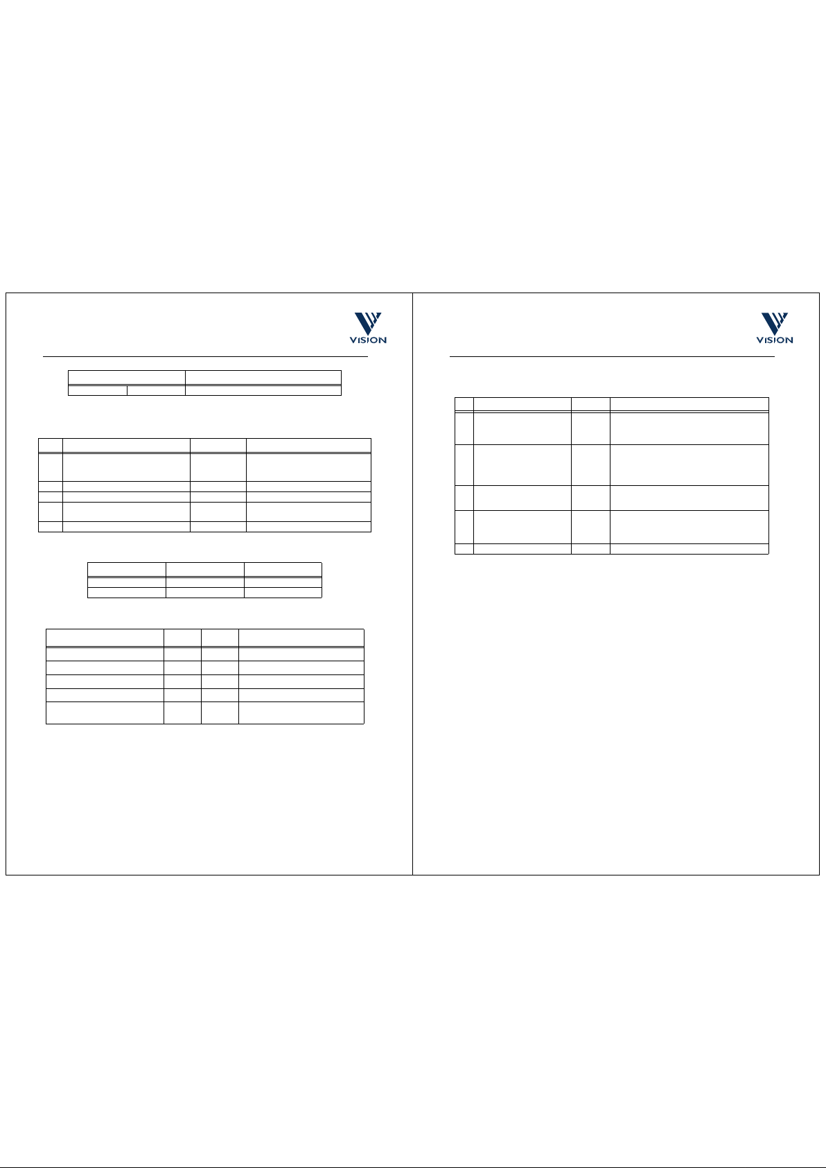
cd38041a.fm 08/10/98 51
VV5409 CMOS Monochrome Sensor Datasheet (Restricted)
Rev 1.0
Commercial In Confidence
[21] - pin_mapping
1 1 Enable FST as the De-bounce switch input
Bit Function Default Comment
0 Map serial-interface register bit values,
on to the QCK, and FST pins
Off
/On
0
1 Serial-Interface Bit for QCK pin 0
2 Serial-Interface Bit for FST pin 0
4:3 Output driver strength select 01 Default setting selects 4mA driver.
Recommended setting is 00.
7:5 Unused 0
Table 6.16 : [21] - pin_mapping
Mapping Enable FST pin QCK pin
0FSTQCK
1 pin_mapping[2] pin_mapping[1]
Table 6.17 : FST/QCK Pin Selection
oeb_composite su5[4] su5[3] Comments
0 0 0 Drive strength = 2mA
0 0 1 Drive strength = 4mA (Default)
0 1 0 Drive strength = 6mA
0 1 1 unallocated
1 x x Outputs are not being driven, there-
fore driver strength is irrelevant
Table 6.18 : Output driver strength selection
FST mode[1:0] FST state
Table 6.15 : FST Modes
cd38041a.fm 08/10/98 52
VV5409 CMOS Monochrome Sensor Datasheet (Restricted)
Rev 1.0
Commercial In Confidence
[23] - op_format
6.6.3 Exposure Control Registers [32 - 47]
There is a set of programmable registers, which control the sensitivity of the sensor. The registers are as
follows:
1. Fine exposure
2. Coarse exposure time
3. Gain
4. Clock division.
The gain parameter does not affect the integration period, rather it amplifies the video-signal at the output
stage of the sensor.
Note:
The external exposure (coarse, fine, clock division or gain) values, do not take effect immediately. Data
from the serial-interface is read by the exposure algorithm at the start of a video-frame. If the user reads an
exposure value from the serial-interface, then the value reported will be the data which has not yet taken
effect with the exposure algorithm, because the serial-interface logic stores locally all the data written to the
sensor.
Between writing the exposure data, and the point at which the data is consumed by the exposure logic, bit-0
of the status register is set. The gain-value is updated a frame later than the coarse, fine, and clock division
parameters, since the gain is applied directly at the video-output stage, and does not require the long set-up
time of the coarse, and fine exposure, and the clock division.
To eliminate the possibility of the sensor-array seeing only part of the new exposure and gain setting, if the
serial-interface communications extends over a frame boundary, the internal re-timing of exposure and gain
data is disabled while writing data to any location in the Exposure page of the serial-interface register map.
Thus if the 5 bytes of exposure, and gain data, is sent as an auto-increment sequence, it is not possible for
the sensor to consume only part of the new exposure, and gain data.
Some parameters have a limited range of values. If any values are programmed out-with this range, they will
be clipped to the maximum value allowed.
Bit Function Default Comment
1:0 Data format select 01 00 - reserved
01 - 4 wire parallel output
10 - 2 wire serial output
11 - 1 wire bit-serial output
2 Embedded SAV/EAV Escape
Sequences
On /
Off
0 0 - Insert Embedded Control Sequences, e.g
Start, and End of Active Video, into Output videodata
1 - Pass-through mode. Output video-data equals
ADC data
3 Complementary Outputs
Off/
On
1 If this bit is set, and 4-wire output is NOT
selected, then the complement of the output,
appears on either 1, or 2 of the output bus lines
4 Enable sample mode
Off/
On
1 If enabled, the data-bus will continuously output a
“96
H
” pattern. With the sensor in this mode, a
user can determine the best point at which to
sample the data
7:5 Unused
Table 6.19 : [23] - op_format
Page 27
cd38041a.fm 08/10/98 53
VV5409 CMOS Monochrome Sensor Datasheet (Restricted)
Rev 1.0
Commercial In Confidence
The table above, details
all
the available gain settings. If the sensor has been configured, as it would be
following a system reset (using RESETB), in either of the CIF video modes, then not all the gain settings will
be available. The lsbit of the gain, written through the serial-interface, is replaced with a fixed 1, the top 3-bits
are preserved. The subsequent gain values available are 1, 3, 5, 7, 9, 11, 13, and 15.
If any of the other 4 video modes is selected, then the control bit which changes the gain-value as above, is
not
set, and the full 4-bit gain-value, is passed to the CAB unaltered. It is possible to write to the tms register,
set this bit, and cause the gain settings to be altered.
Register
Index
Bits Function Default Comment
32 0:0 Fine MSB exposure value 0 Maximum mod e dependent
33 7:0 Fine LSB exposure value
34 0:0 Coarse MSB exposure value 302 Maximum mode dependent
35 7:0 Coarse LSB exposure value
36 3:0 Gain value 0 See Table 6.21
37 1:0 Clock divisor value 0 See Table 6.22
Table 6.20 : Exposure, Clock Rate and Gain Registers
Gain Binary code Actual signal gain Gain Binary code Actual signal gain
0000
2
0.500 1000
2
0.533
0001
2
1.000 1001
2
1.143
0010
2
0.667 1010
2
0.727
0011
2
2.000 1011
2
2.667
0100
2
0.571 1100
2
0.615
0101
2
1.333 1101
2
1.600
0110
2
0.8 00 1110
2
0.889
0111
2
4.0 00 1111
2
8.000
Table 6.21 : System Analog Video Gain Values
Clock Divisor Setting Pixel Clock Divisor
00
2
2
01
2
4
10
2
8
11
2
16
Table 6.22 : Clock Divisor Values
cd38041a.fm 08/10/98 54
VV5409 CMOS Monochrome Sensor Datasheet (Restricted)
Rev 1.0
Commercial In Confidence
6.6.4 Serial-Interface Setup Registers [108-111]
6.6.5 System Registers -Addresses [112 - 127]
[112 - 114] - Black Calibration Registers
The sensor is equipped with an automatic function which continually monitors the output black level, and recalibrates, if it has moved out of programmable range. The user is advised to disable the automatic function
before attempting to write any of these parameters.
Register
Index
Bit Function Default Comment
108 0 Re-Initiate Auto-load Sequence 0 Initiate Auto-Load (where used), if
bit high, goes from high to low.
Auto-load token-bit must be high for
auto-load to be triggered
108 1 Auto-load Token
No Token
/ Token
0 Initiate, if low to high transition on bit
i.e. auto-load token received. Reset
to zero on completion of auto-load
i.e. token passed on to next device
7:3 unused 0
Table 6.23 : [108] - Serial-Interface Setup Register, sf_setup
Register
Index
Bits Function Default Comment
109 7:0 next_de v_addr - Serial-Interface Address of next Device
in auto-load daisy chain (where used).
Default is the sensor’s 7-bit serial
address plus 4
Table 6.24 : [109] - Serial Address of next Device in Daisy-Chain
Register
Index
Bits Function Default Comment
112 3 :0 bcal_window 0 Black Level Monitor/Calibration
Window Sizes
113 7 :0 bcal0 128 DAC B0 value
114 7 :0 bcal1 128 DAC B0 value
Table 6.25 : Black Calibration Registers
Register
Index
Bit Function Default Comment
1:0 bcal_win 0 Black Calibration monitor window size
Table 6.26 : [112] - Black Level Monitor/Calibration Window Sizes
Page 28
cd38041a.fm 08/10/98 55
VV5409 CMOS Monochrome Sensor Datasheet (Restricted)
Rev 1.0
Commercial In Confidence
[117 - 118] - Control Registers 0 and 1- CR0 and CR1
2 Monitor window size set by
serial-interface
communication
Yes/
No
0 Allow the serial-interface to set the
Black Calibration monitor window size
directly
3 Narrow Black Calibration
target window
Yes
/No
0 By default the target window size for
the Black Calibration (calibration
phase) is set to the widest position
7:4 used 0
Bit Function
PAL/NTSC
value
Default Comment
0 Enable bit line clamp
Off
/On
00
1 New PXRDB scheme
Off
/On
00
2 I nhib it horizontal shift register
Off
/On
00
3 Enable anti-blooming
protection
Off
/On
10
4 Inhibit OSA fast reset
Off
/On
00
5 E xte rnal bit line white
reference
Off
/On
00
6 CDSH Mo de
New
/Old
0 0 By asserting this control bit,
the falling edge of CDSH is
forced to occur earlier in the
line timing
7 V CDSH Voltage
3.0 / 3.9V
1 0 0 - VCDSH = 3.0 V
1 - VCDSH = 3.9 V
Table 6.27 : [117] - Control Register CR0
Bit Function
PAL/NTSC
value Default Comment
0 Stand-by
Off
/On
0 0 Powers down ALL analogue
circuitry
Table 6.28 : [118] - Control Register CR1
Register
Index
Bit Function Default Comment
Table 6.26 : [112] - Black Level Monitor/Calibration Window Sizes
cd38041a.fm 08/10/98 56
VV5409 CMOS Monochrome Sensor Datasheet (Restricted)
Rev 1.0
Commercial In Confidence
Notes:
1. The signal enabling the external ADC functionality, is the logical OR of CR0 [0] bit and the invert of the
ADCVDD pin
2. The low-power select signal for the analogue circuitry, is the logical OR of PD0 [0] and Setup0 [0].
[119] - ADC Setup Register AS0
1 Power Down - ADC
Off
/On
00
2 Power Down - ADC Top
Reference
Off
/On
00
3 Power Down - AVO Output Buffer
Off
/On
00
4 B1 Offset DAC Gain Select
Low (x1)
/ High (x2)
10
5 Inhibit Quiet ADC Signal
Off
/ On
00
7:6 RST/MRST Phase Delay Setting
0
°
/ 90° / 180° / 270
°
01 00 00: Phase Delay = 0° (Default)
01: Phase Delay = 90
°
10: Phase Delay = 180
°
11: Phase Delay = 270
°
Bit Function Default Comment
1:0 ADC Clock Fine Delay Setting
0 ns
/ 4 ns / 8 ns / 16 ns
00 00: Clock Delay = 0 ns (Default)
01: Clock Delay = 4 ns
10: Clock Delay = 8 ns
11: Clock Delay = 16 ns
3:2 ADC Clock Phase Delay Setting
0° /
90
°
/ 180° / 270
°
01 00: Phase Delay = 0
°
01: Phase Delay = 90° (Default)
10: Phase Delay = 180
°
11: Phase Delay = 270
°
5:4 PCK Clock Fine Delay Setting
0 ns
/ 4 ns / 8 ns / 16 ns
00 00: Clock Delay = 0 ns (Default)
01: Clock Delay = 4 ns
10: Clock Delay = 8 ns
11: Clock Delay = 16 ns
6 ADC Clock Generator Setting
Fast /
Slow
1 1 - CIF Mode
0 - CCIR-601/656. NTSC, PAL modes
7 U nused
Table 6.29 : [119] - ADC Setup Register AS0
Bit Function
PAL/NTSC
value Default Comment
Table 6.28 : [118] - Control Register CR1
Page 29
cd38041a.fm 08/10/98 57
VV5409 CMOS Monochrome Sensor Datasheet (Restricted)
Rev 1.0
Commercial In Confidence
[120] - Analogue Test Register AT0
[121] - Microphone Amplifier Setup Register AT1
Bit Function
PAL/NTSC
value Default Comment
0 Enable test output on AVO
Off
/ On
0 0 Internal test mode
1 M onitor bitline voltage or
input to the Column Sample
Hold
Vx
/ V1
0 0 Internal test mode
2 M onitor co lumn 354 or 355
354
/ 355
0 0 Internal test mode
3 Spare 0 0
4 OSA Pre-Charge Timing
LRPC
/(LRPC + PRPC)
1 0 0 - Line Rate Pre-Charge (LRPC)
1 - LRPC + PIx Rate Precharge
(PRPC)
5 OSA Pixel Rate Pre-Charge
Hi Duration
4 ns
/ 8 ns
0 0 0 - PRPC Width = 4 ns
1 - PRPC Width = 8 ns
6 OSA Pre-Charge Voltage
VDD
/ VDD - 0.5 V
0 0 0 - Pre-Charge Voltage = VDD
1 - Pre-Charge Voltage = VDD -
0.5 V
7 V RT Voltage
2.5 V
/ 2.75 V
0 0 0 - VRT = 2.5 V
1 - VRT = 2.75 V
Table 6.30 : [120] - Analogue Test Register AT0
Bit Function Default Comment
3:0 Microphone Amplifier Gain 0 See T able 6.32
4 D igitise Microphone Am pl ifier Output
Off
/ On
0 If this bit is selected, the ADC will
convert the output from the microphone
amplifier
5 Pad to supply analogue input to
Microphone amplifier
On
/ Off
0 If this bit is1, the pad will supply a signal
holdpix which will inhibit the ADC
operating. If this bit is 0, the holdpix
input is connected to the input of the
microphone amplifier
6 Power down microphone amplifier
Off
/ On
0
cd38041a.fm 08/10/98 58
VV5409 CMOS Monochrome Sensor Datasheet (Restricted)
Rev 1.0
Commercial In Confidence
The register values shown in Table 6.32 correspond to actual gain values, where Actual gain = V
out/Vin
.
Register: at1 on VV5409. Default is 15.
6.7 Types of serial interface messages
This section gives guidelines on the basic operations of reading data from, and writing data to, the serialinterface.
The serial-interface supports variable length messages. A message may contain no data-bytes, one databyte, or many data-bytes. This data, can be written to , or read from common, or different locations within the
sensor. The range of instructions available are detailed below.
• Write no data-byte, only sets the index for a subsequent read message
• Single location, multiple data write, or read for monitoring (real time control)
• Multiple location, multiple data read, or write, for fast information transfers.
Examples of these operations are given below. A full description of the internal registers, is given in the
previous section. For all examples, the slave address used is 32
10
for writing, and 3310 for reading. The write
address includes the read/write bit (the lsb), set to zero while this bit is set in the read address.
6.7.1 Single location, single data write
When a random value is written to the sensor, the message will look like this :
In this example, the
fineH
exposure register (index = 3210), is set to 8510. The r/w-bit is set to zero for writing,
and the
inc
bit (msbit of the index byte), is set to zero, to disable automatic incrementation of the index after
writing the value. The address index is preserved and may be used by a subsequent read. The write message
is terminated with a stop condition from the master.
7 Microphone Amplifier Digitisation Mode
EAV
/ Always
0 Digitise the MicrophoneMicrophone
output, either only during the end of
active video embedded escape
sequence, or always
Gain register0123456789101112131415
Actual gain 1 2 4 8 2 4 8 16 4 8 16 32 8 16 32 64
Table 6.32 : Audio Gain register Settings
Bit Function Default Comment
Table 6.31 : [121] - Microphone Amplifier Setup Register AT1
Figure 6.4 :
Single location, single write
S
20
10
A 0 32
10
A
85
10
A
P
Start
Device
Ack
address
Index
Data
Stop
Page 30
cd38041a.fm 08/10/98 59
VV5409 CMOS Monochrome Sensor Datasheet (Restricted)
Rev 1.0
Commercial In Confidence
6.7.2 Single location, single data read
A read message always contains the index used to get the first byte.
This example assumes that a write message has already taken place, and the residual index value is 32
10
.
A value of 85
10
is read from the
fineH
exposure register. Note that the read message is terminated with a
negative acknowledge (A
) from the master; it is not guaranteed that the master will be able to issue a stop
condition, at any other time during a read message. This is because, if the data sent by the slave is all zeros,
the
SDA
line cannot rise, which is part of the stop condition.
6.7.3 No data write, followed by same location read
When a location is to be read, but the value of the stored index is not known, a write message with no data
byte must be written first, specifying the index. The read message then completes the message sequence.
To avoid relinquishing the serial-bus to another master, a repeated start condition is asserted between the
write, and read messages. In this example, the
gain
value (index = 3610) is read as 1510.
As mentioned in the previous example, the read message is terminated with a negative acknowledge (A
) from
the master.
6.7.4 Same location, multiple data write
It may be desirable to write a succession of data to a common location. This is useful when the status of a
bit,(e.g. requesting a new black calibration), must be toggled.
The message sequence indexes
setup1
register. If bit 1 is toggled low, high low this will initiate a fresh black
calibration. This is achieved by writing three consecutive data bytes to the sensor. There is no requirement
to re-send the register index before each data byte.
Figure 6.5 : Single location, single read
S 2110 A 0 3210 A 85
10
A P
Start
Device
Ack
address
Index Data
Stop
Figure 6.6 : No data write followed by same location read
S
A
Sr A
A
A
P
21
10
36
10
21
10
36
10
1510A
0
0
No data write Re ad index and data
SA 010AA A20
10
17
10
2
10
010A0
Write
setup1
Turn off ABC
Toggle “Force Black Cal.”
P
Figure 6.7 : Same location multiple data write
cd38041a.fm 08/10/98 60
VV5409 CMOS Monochrome Sensor Datasheet (Restricted)
Rev 1.0
Commercial In Confidence
6.7.5 Same location, multiple data read
When an exposure related value (
fineH, fineL, coarseH, coarse L, gain, or clk_div
) is written, it takes effect
on the output at the beginning of the next video frame, (remember that the application of the
gain
value is a
frame later than the other exposure parameters). To signal the consumption of the written value, a flag is set
when any of the exposure, or gain registers, are written, and is reset at the start of the next frame. This flag
appears in
status0
register, and may be monitored by the bus master. To speed up reading from this location,
the sensor will repeatedly transmit the current value of the register, as long as the master acknowledges each
byte read.
In the next example, a
fineH
exposure value of 0 is written, the status register is addressed (no data byte),
and constantly read until the master terminates the read message.
6.7.6 Multiple location write
If the automatic increment bit is set, (msb of the index byte), it is possible to write data bytes to consecutive,
adjacent internal registers, without having to send explicit indexes prior to sending each data byte. An autoincrement write to the black calibration DAC registers, with their default values is shown in the following
example.
6.7.7 Multiple location read
In the same manner, multiple locations can be read with a single read message. In this example the index is
written first, to ensure the exposure related registers are addressed, and then all six are read.
SA 0AA A
2010331020
10
010A0
Sr
AAA A
21
10
0
10
111A0
Sr
Write
fineL
with zero
Address the status0 register
A10A
Read continuously...
...until flag reset
P
Figure 6.8 :
Same location, multiple data read
SA
128
16
AAA
201011310128
16
1
Incremental write
P
Figure 6.9 :
Multiple location write
Page 31
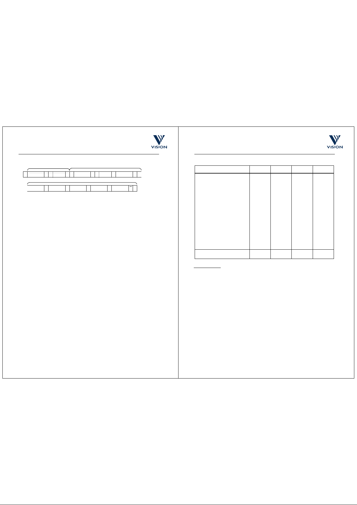
cd38041a.fm 08/10/98 61
VV5409 CMOS Monochrome Sensor Datasheet (Restricted)
Rev 1.0
Commercial In Confidence
Note that a stop condition is not required after the negative acknowledge from the master.
Incremental read
SAA20
10
32101 Sr 2110AA32101
fineH
A
A
P
fineL coarseH coarseL gain clk_div
AAAA
No data write
Incremental read
Figure 6.10 : Multiple location read
cd38041a.fm 08/10/98 62
VV5409 CMOS Monochrome Sensor Datasheet (Restricted)
Rev 1.0
Commercial In Confidence
6.8 Serial-Interface Timing
Parameter Symbol Min. Max. Unit
SCL clock frequency fscl 0 100 kHz
Bus free time between a
stop
and a
start
tbuf TBD - us
Hold time for a repeated
start
thd;sta 80 - nS
LOW period of SCL tlow 320 - nS
HIGH period of SCL thigh 160 - nS
Set-up time for a repeated
start
tsu;sta 80 - nS
Data hold time thd;dat 0 - us
Data Set-up time tsu;dat 0 - ns
Rise time of SCL, SDA (from V
IL
=
0.2VDD - V
IH
= 0.8VDD)
tr - 300 (Note 1) ns
Fall time of SCL, SDA ( from V
H
= 2.4v -
V
L
= 0.5v)
tf - 300 (Note 1) ns
Set-up time for a
stop
tsu;sto 80 - nS
Capacitive load of each bus line (SCL,
SDA)
Cb - 200 pF
Table 6.33 : Serial Interface Timing Characteristics
Notes on Table 6.33:
(1) With 200pF capacitive load. It is recommended that pull-up resistors of 2.2k are fitted to both SDA and
SCL lines (see Section 13.).
Page 32
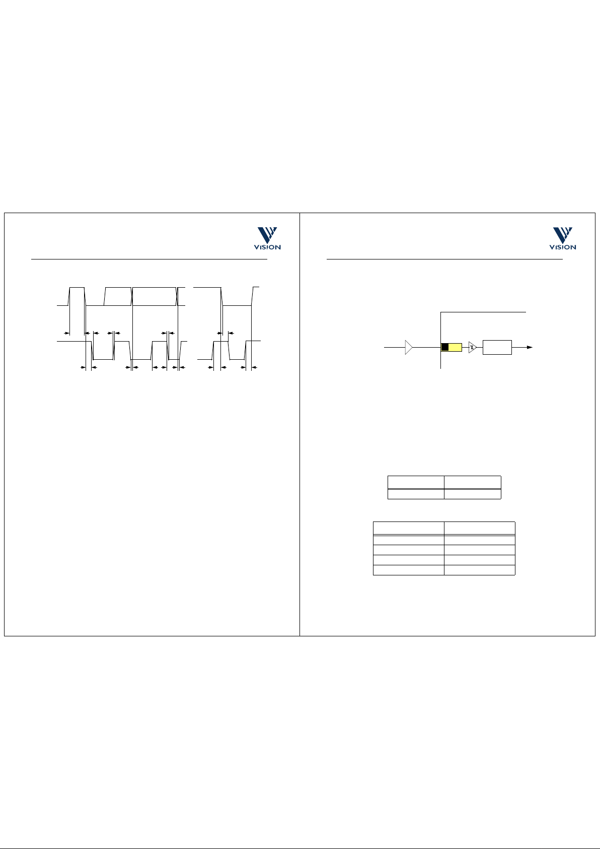
cd38041a.fm 08/10/98 63
VV5409 CMOS Monochrome Sensor Datasheet (Restricted)
Rev 1.0
Commercial In Confidence
SDA
SCL
thd;sta
tr
thightftsu;datthd;dat tsu;sta tsu;sto
...
...
thd;statlowtbuf
stopstartstop start
All values referred to the minimum input lev el (high) = 3.5V, and maximum input level (low) = 1.5V
Figure 6.11 : Serial Interface Timing Characteristics
cd38041a.fm 08/10/98 64
VV5409 CMOS Monochrome Sensor Datasheet (Restricted)
Rev 1.0
Commercial In Confidence
7. Clock Signal
VV5409 system clock is supplied from an external clock source, directly driving the CLKI pin. This pin has an
internal Schmitt buffer. There is no support for a crystal oscillator.
If the clock is generated for the video sensor by a host controller, it must be active during serial-interface
communications for at least 16 clock cycl es, before t he serial communica tions start bit, and at least 1 6 cycles
after the serial communications stop bit.
The synchronisation input, SIN, synchronises the clock divider logic in addition to the main clock generation,
and the video timing control block.
For greater flexibility the pixel frequency (for 4 wire output format) can be divided by 2, 4, 8, or 16. The pixel
clock frequency is a further factor of 2 down for 2-wire, or a factor of 4 for bit-serial mode.
The clock signal must be a square wave with a 50% (±10%) mark:space ratio. Table 7.1 specifies the
maximum pixel clock frequencies for the module. Table 7.2 specifies the relationship between the input clock,
CLKI, and the pixel clock frequency for the different settings of the sensor’s internal clock divider.
This translates into a maximum input clock frequency of 14.31818 MHz if a pixel clock divisor of 2 is used
(the default - Table 7.2).
MHz
Maximum Pixel Rate 7.15909
Table 7.1 : Maximum Pixel Clock Rate
Clock Divisor Setting Pixel Clock Divisor
00
2
2
01
2
4
10
2
8
11
2
16
Table 7.2 : Clock Divisor Values
VV5409
CLK
Figure 7.1 :
External Clock Source
CLKI
Clock
Source
CLOCK
DIVISION
Page 33
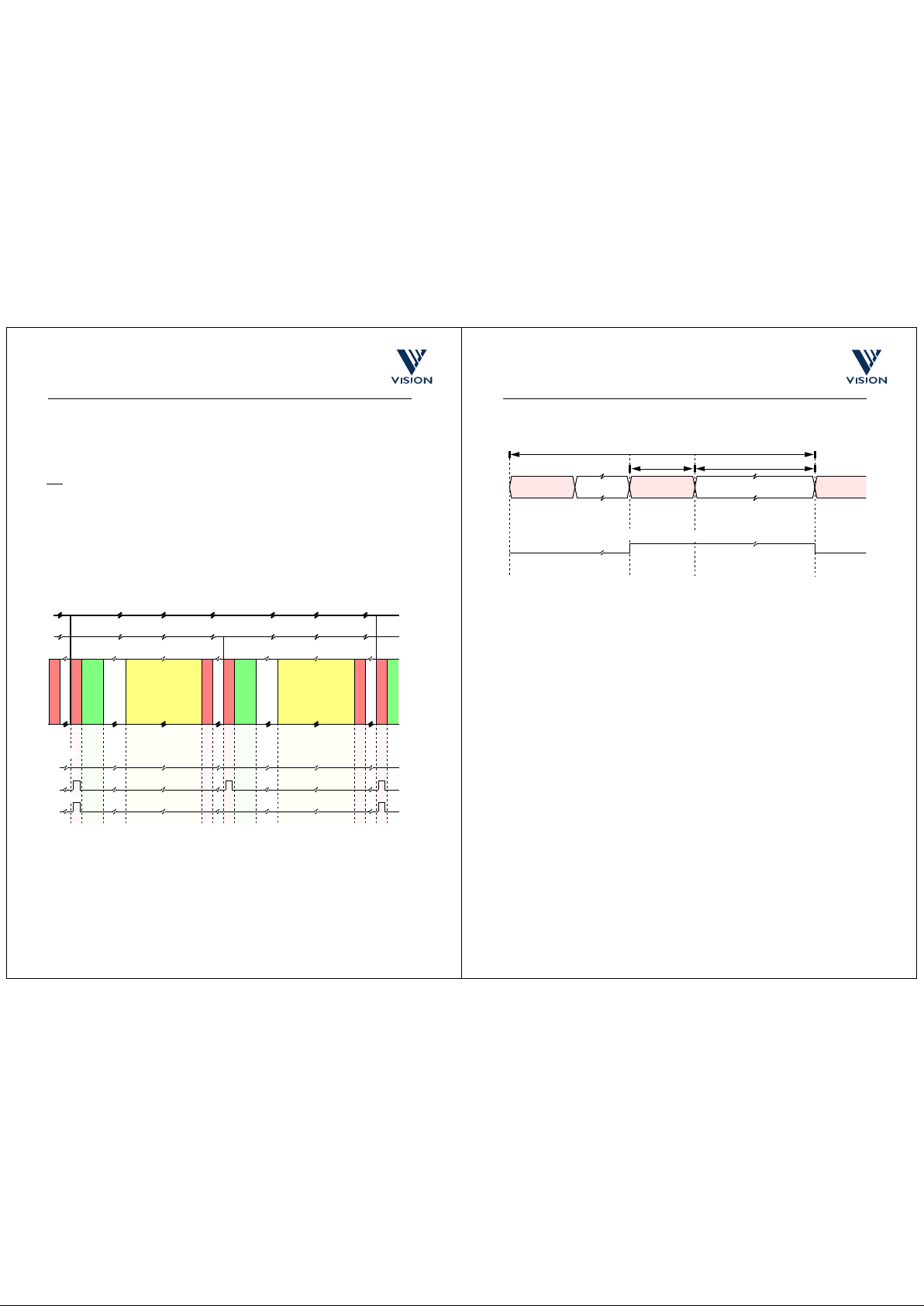
cd38041a.fm 08/10/98 65
VV5409 CMOS Monochrome Sensor Datasheet (Restricted)
Rev 1.0
Commercial In Confidence
8. Synchronising Multiple Cameras
A rising edge on the SIN pin re-synchronises the sensors internal video timing logic and clock generators to
6 pixels before the end of the start of frame control sequence in line 0. By supplying a rising edge to SIN once
per frame, 2 cameras can be synchronised together. Via the serial interface the function of the FST pin can
be modified to generate the required synchronisation output signal (SNO). Synchronising cameras is done
by setting one camera up as the master and feeding its SNO signal to the SIN input of the other cameras.
Note
: The correct functionality of the SNO output has not been verified.
The internal logic is designed such that if the rising edge of SIN occurs in the correct place, 6 pixels (for the
default pixel counter reset value) before the end of the start of frame control sequence, the sensor’s operation
is unaffected. Otherwise the video timing and clock generation will be reset. The following frame should be
treated as corrupt.
SIN is sampled internally by the system clock, CKI. If all cameras are supplied with the same clock signal
then the reset generated by SIN will synchronise all the cameras to the sa me point in time. However, if the
cameras being synchronised are running at the same frequency but each camera has its own crystal, then
there could be up to one system clock period of skew between the cameras. This skew will vary over time
due to the slight mismatches between frequencies of the different crystals.
Start of Field
Black Lines
Blanking Lines
Visible Line s
End of Field
Blanking Lines
Start of Field
Black Lines
Blanking Lines
Visible Line s
End of Field
Blanking Lines
Blanking Lines
Start of Field
1st Field 2nd Field
1 Frame
(ii) On
Frame/Field Format:
Figure 8.1 : FST and SNO Signals - Frame / Field Level Timing
End of Field
FST:
(ii) Off
(iii) SNO
cd38041a.fm 08/10/98 66
VV5409 CMOS Monochrome Sensor Datasheet (Restricted)
Rev 1.0
Commercial In Confidence
SAV
EAV
EAV
Status Information
Synchronisation Output (SNO) from the master sensor (functionality not verified)..
1 Line
356/306 Pixels
6 Pixels
Figure 8.2 :
Synchronisation Waveforms - Line Level Timing.
Start of Field Line Format:
Page 34
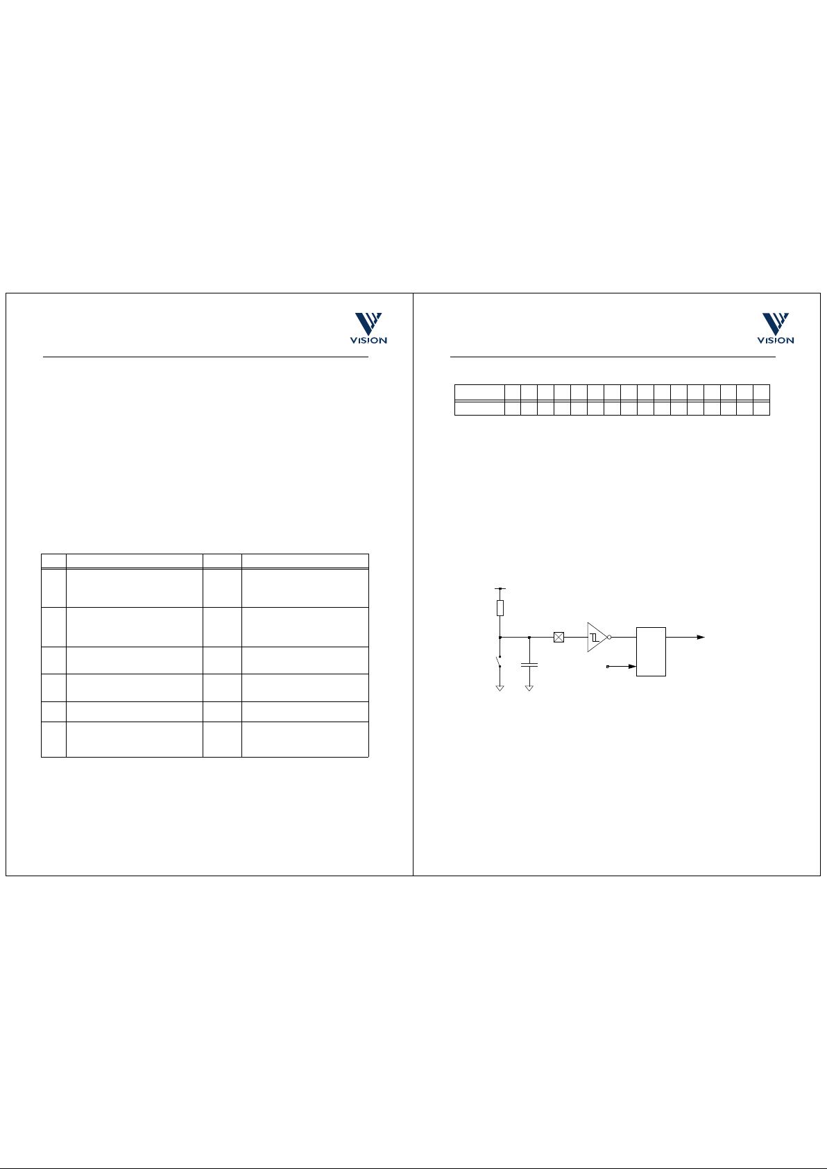
cd38041a.fm 08/10/98 67
VV5409 CMOS Monochrome Sensor Datasheet (Restricted)
Rev 1.0
Commercial In Confidence
9. Other Features
9.1 Microphone Amplifier
The internal Microphone amplifier, comprises 3 separate amplifiers. The first 2 in the chain have
programmable gain values (x 1, x 2, x 4 and x 8). The third amplifier is configured as a voltage follower, and
drives the AOUT pin. Pin AIN is the input to the first amplifier in the chain.
The gain of each of the first two amplifiers, is independently controllable through the serial-interface register
at1
. There are 7 possible overall system gains: x 1, x 2, x 4, x 8, x 16, x 32, and x 64.
The input, and output voltage ranges, should lie within the ADCtop and ADCbot voltages. The mid-point of
these two references is used as the virtual ground for the first two amplifiers.
The output amplifier, can drive a 2v peak-peak load (1.3v DC offset) with 1k ohm minimum impedance. The
compensation capacitor for the output amplifier is external. By varying the AC-coupling capacitor on the input,
and the compensation capacitor on the output, the frequency response of the amplifier can be modified.
Input, and output voltage ranges are from the voltage reference ADCbot to the ADCtop voltage reference.
The Microphone amplifier setup register, also allows the amplifiers to be powered-down, and there is an
option to multiplex internally the output of the final amplifier during the embedded “End-of-Line” sequence,
on to the input of the 8-bit ADC used to digitise pixel-data. The digitised data for 2 consecutive samples,
appears as the 2 supplementary bytes in the 6-byte end of line embedded escape sequence. Thus the videodata stream contains 2 consecutive samples of the output of the Microphone amplifier once per line.
The register values shown in Table 9.2 correspond to actual gain values. Register: at1 on VV5409. Default
Bit Function Default Comment
1:0 2-bit gain value for 1st gain stage, a0[1:0] 00 00: 1st Stage Gain = x 1
01: 1st Stage Gain = x 2
10: 1st Stage Gain = x 4
11: 1st Stage Gain = x 8
3:2 2-bit gain value for 2nd gain stage, a1[1:0] 00 00: 2nd Stage Gain = x 1
01: 2nd Stage Gain = x 2
10: 2nd Stage Gain = x 4
11: 2nd Stage Gain = x 8
4 D igitise Microphone Am pl ifier Output
Off
/ On
0 If this bit is selected, the ADC will
convert the output from the microphone
amplifier
5 Pad to supply analogue input to
Microphone amplifier
Off /
On
1 If this bit is reset, the pad will supply a
signal holdpix which will inhibit the ADC
operating
6 Power down microphone amplifier
Off
/ On
0
7 Microphone Amplifier Digitisation Mode
EAV
/ Always
0 Digitise the Microphone output, either
only during the end of active video
embedded escape sequence, or
always
Table 9.1 : [121] - Microphone Amplifier Setup Register AT1
cd38041a.fm 08/10/98 68
VV5409 CMOS Monochrome Sensor Datasheet (Restricted)
Rev 1.0
Commercial In Confidence
is 15.
9.2 Debounced Switch Input
VV5409 provides a special debounced digital input pin, FST/DIN, for switches. When FST/DIN is enabled as
a debounced switch input, a low on the DIN sets a set/reset latch. The value of this latch, is part of status
register
status0,
and thus can be observed through the serial-interface register data contained in the start-
of-field line. At the end of a start-of-field line, the latch is reset.
This input is primarily intended for a user to “mark” the required frame, by pressing a button perhaps on a
remote camera head.
This feature can be enabled by bits 6 and 7 of the fg_modes register (see Table 6.11).
9.3 Serial-Interface Programmable Pins
The FST and QCK can be re-configured to follow the values of bits 1 and 2 in the serial-interface register
pin_mapping
. This is to allow remote control of a electro-mechanical system, for example two different zoom
settings, in a remote camera head through the serial-interface.
Gain register0123456789101112131415
Actual gain 1 2 4 8 2 4 8 16 4 8 16 32 8 16 32 64
Table 9.2 : Audio Gain register Settings
DIN
To status
reg
status0
C
filterRpullup
Figure 9.1 :
Debounced Switch Input
SRQ
QN
Reset at end of
status line
Inverting
Schmitt
Buffer
Set/Reset
Latch
Switch
Page 35
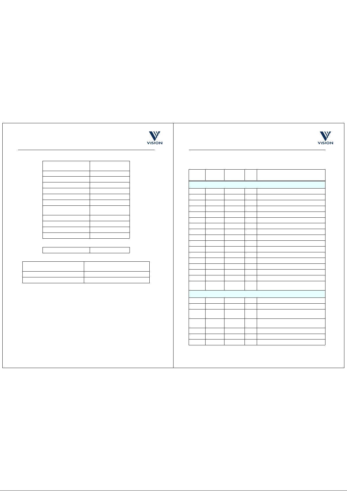
cd38041a.fm 08/10/98 69
VV5409 CMOS Monochrome Sensor Datasheet (Restricted)
Rev 1.0
Commercial In Confidence
10. Detailed specifications
Table 10.3 : VV5409 Audio Pre-amplifier
Image Format 306 x 244 pixels (NTSC)
356 x 292 pixels (PAL)
Pixel Size 9.0x 8.25µm
Technology 0.6µm 2 level metal CMO S
Array Format CIF
Exposure control 25000:1
Sensor signal / Noise ratio TBD
Supply Voltage 5.0v DC +/-5%
Package type 48LCC (sampling)
48BGA (production)
Operating Temp. range 0
o
C - 40oC
Logic 0 input 0.2 x Vdd Max
Logic 1 input 0.8 x Vdd Min
Serial interface frequency range 0-100kHz
Table 10.1 : VV5409 Specifications
Current Consumption TBD
Table 10.2 : VV5409 Specifications
Audio pre-amp output rating 2v peak-peak
1.3v DC offset
Audio pre-amp output Min. Impedance 1k ohms
Audio pre-amp input AC coupled 2v peak-peak max
cd38041a.fm 08/10/98 70
VV5409 CMOS Monochrome Sensor Datasheet (Restricted)
Rev 1.0
Commercial In Confidence
11. Pinouts and pin descriptions
11.1 Sensor pin list
Pin No.
(48LCC)
Pin No.
(48BGA)
Name Type Description
POWER SUPPLIES
1A4AVCCPWRPower
48 C4 AGND GND Ground
43 B2 DVDD PWR Digital Power
44 C3 DVSS/Dsub GND Digital Ground
6 C5 AVDD P WR Output stage power
5 A6 AVSS GND Output stage ground
7 A7 VVDD PWR Analogue output buffer power
9 B7 VVSS GND Analog ue output buffer ground
14 D5 ADCVDD PWR ADC power
10 C6 ADCVSS GND ADC ground
19 G7 VDD1 PWR Power
30 F3 VDD2 PWR Power
36 E2 VDD3 PWR Power
20 F6 VSS1 GND Ground
29 G2 VSS2 GND Ground
37 D1 VSS3 GND Ground
- D4 Die Paddle GND Die paddle on BGA package only. Connect to
AGND.
ANALOGUE SIGNALS
45 A2 VBLOOM OA Anti-blooming pixel reset voltage
46 B3 VBLTW OA Bitline test white level reference
47 A3 VBG OA I nterna lly generated bandga p reference volt age
1.22V
2B4VCM/
VREF2V5
OA Common-mode input for OSA and Internally
generated 2.5 V reference voltage
3 A5 VRT IA Pixel reset voltage
4 B5 VCDSH IA Correlated Double Sampling reference
8 B6 DNC - Reserved
Page 36
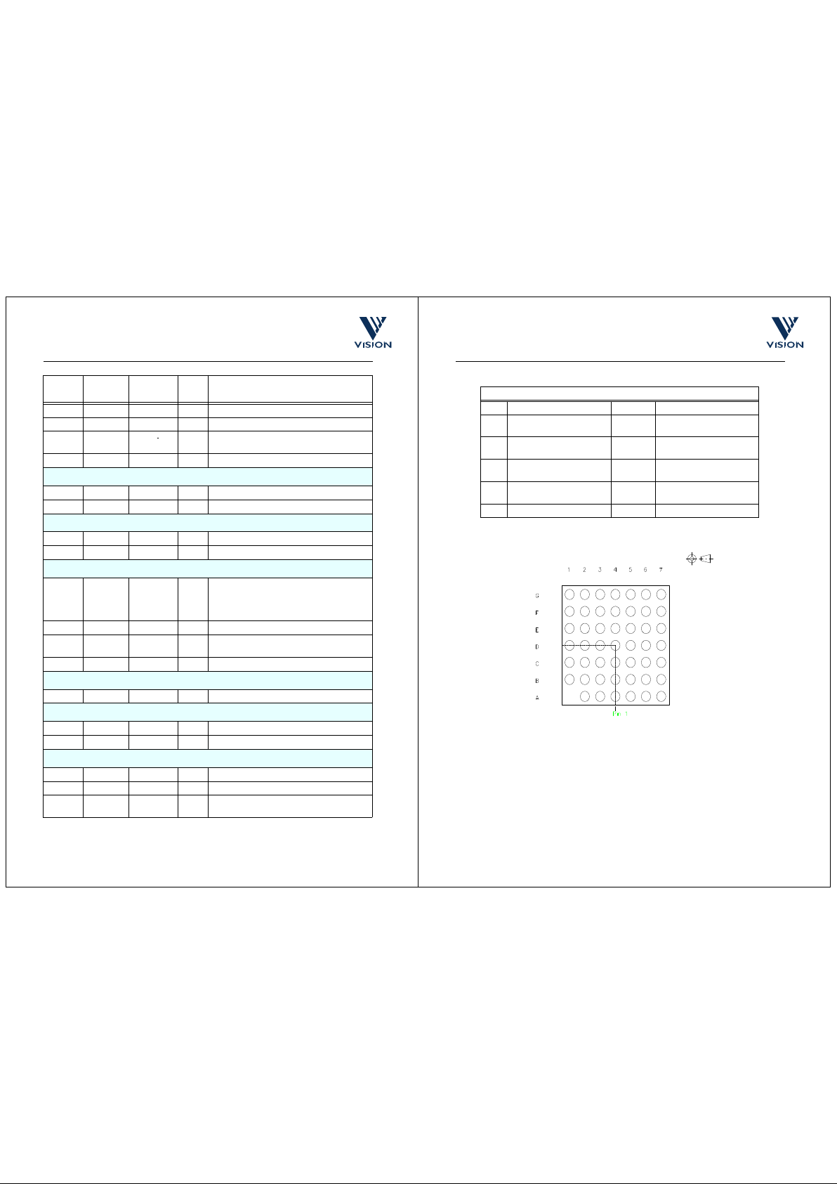
cd38041a.fm 08/10/98 71
VV5409 CMOS Monochrome Sensor Datasheet (Restricted)
Rev 1.0
Commercial In Confidence
11 C7 ADCbot IA Bottom voltage reference for ADC
12 D6 AIN IA Analogue input for Audio pre-amp
13 D7 ADCtop/
TopRef
OA Internally generated top voltage reference for ADC
15 E7 AOUT OA Analogue output from Audio pre-Amp
DIGITAL CONTROL SIGNALS
16 E6 SIN ID↓Reserved
17 F7 RESETB ID↑System Reset. Active Low.
SERIAL-INTERFACE
42 C2 SCL ID↑Serial bus clock (input only)
41 B1 SDA BI↑Serial bus data (bidirectional, open drain)
DIGITAL VIDEO INTERFACE
39
38
35
34
C1
D2
E1
E3
D[3]
D[2]
D[1]
D[0]]
ODT Tri-stateable 4-wire output data-bus. D[3] is the
most significant bit
33 F1 QCK ODT Tri-stateable data qualification clock
40 D3 FST/DIN ODT Tri-stateable Frame start signal/Debounced switch
input
32 F2 LST ODT Line start signal
SYSTEM CLOCKS
31 G1 CLKI ID Oscillator input
NOT CONNECTED (
48LCC
)
18 - NC Not connected
21-28 - NC Not connected
NOT CONNECTED (
48BGA
)
- E4, E5 NC Not connected
- F4, F5 NC Not connected
- G3, G4, G5, G6NC Not connected
Pin No.
(48LCC)
Pin No.
(48BGA)
Name Type Description
cd38041a.fm 08/10/98 72
VV5409 CMOS Monochrome Sensor Datasheet (Restricted)
Rev 1.0
Commercial In Confidence
Table 11.1 : Pin descriptions for VV5409
11.2 48BGA pinout
Figure 11.1 : 48BGA pinout (viewed from die side)
Key
A Analogue Input D Digital Input
OA Analogue Output ID
↑
Digital input with internal pullup
BI Bidirectional ID
↓
Digital input with internal pulldown
BI↑Bidirectional with internal pull-upOD Digital Output
BI↓Bidirectional with internal pull-
down
ODT Tri-stateable Digital Output
DNC Non-user pin:
Do not connect
NC Not connected
Table 11.2 : Key to Pin descriptions for VV5409
Drawing
not to
scaleNCNCNCNCNCNCNCNC
Page 37
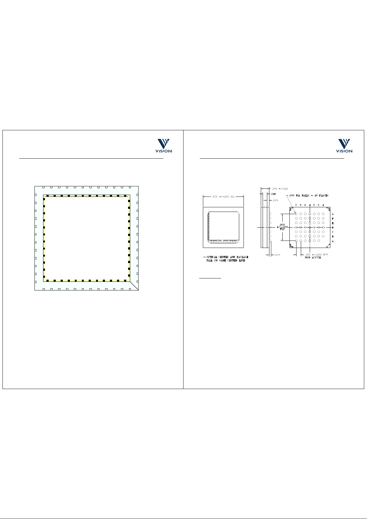
cd38041a.fm 08/10/98 73
VV5409 CMOS Monochrome Sensor Datasheet (Restricted)
Rev 1.0
Commercial In Confidence
11.3 48LCC Pinout
Figure 11.2 : VV5409 Pinout in 48 LCC Package
Notes on Figure 11.2:
1. Diagram viewed from above
2. (*) - Paddle Connections
3. NC = Not Connected
4. DNC = Do not connect (Non-user pin)
CLKI
LST
D[0]
D[1]
VDD3
VSS3
DVSS/Dsub
VBLTW
VBG
VCDSH
AVCC
AGND (*)
VVSS
ADCVSS (*)
ADCVDD
VDD1
VSS1
AOUT
7
8
6
543214847464544
42
41
38
9
10
11
12
13
14
15
16
17
1920212223242526272829
32
33
34
35
36
37
D[2]
D[3]
FST
SDA
SCL
VCM / VREF2V5
AVSS
VBLOOM
ADCBot
40
39
18
30
31
43
DNC
AVDD
QCK
VVDD
RESETB
SIN
TopRef/
AIN
VRT
VSS2
VDD2
NC
DVDD
NCNCNCNCNCNCNC
NC
ADCTop
cd38041a.fm 08/10/98 74
VV5409 CMOS Monochrome Sensor Datasheet (Restricted)
Rev 1.0
Commercial In Confidence
12. Package dimensions
12.1 48BGA (400G)
Figure 12.1 : BGA Package dimensions
Additional notes:
1. All dimensions given in inches.
2. The height of the sensor photoplane (upper die surface) above the bottom of the BGA package =
1.053mm+/- 0.0254mm
3. After reflow, the separation between the PCB surface and the bottom of the BGA package will be
0.4826mm +/- 0.0254mm (when recommended footprint is used, as per the example detailed in the
Applications Note: ‘Single Standard (NTSC or PAL) CMOS Camera Design Guidelines using the
VV6407 sensor and AP1 co-processor’).
4. The optical centre of the die is located at the centre of the package.
Page 38
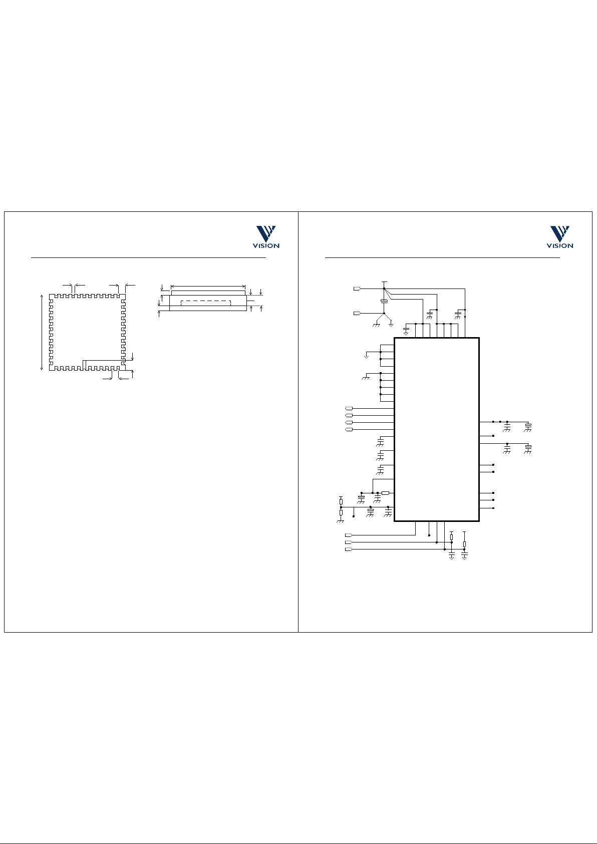
cd38041a.fm 08/10/98 75
VV5409 CMOS Monochrome Sensor Datasheet (Restricted)
Rev 1.0
Commercial In Confidence
12.2 48LCC
Figure 12.2 : 48LCC package dimensions and optical centering
0.51
TYP
1.56 TYP
2.16
PIN 1
1.016 PITCH TYP
14.22
Viewed from below
0.53
0.55
Glass Lid
Base
Viewed from side
Die
0.86
0.5
13.7
The optical array is centred within the
package to a tolerance of ± 0.2 mm, and
rotated no more than ± 0.5
o
Tolerances on package dimensions ±10%
Glass lid placement is c ont rolled so that no
package overhang exists
All dimensions in mill im et res
cd38041a.fm 08/10/98 76
VV5409 CMOS Monochrome Sensor Datasheet (Restricted)
Rev 1.0
Commercial In Confidence
13. Suggested VV5409 support circuit
Figure 13.1 : Suggested schematic for VV5409
C1
C4
IC1
E7
E2F2G1A4A2A5C5A3B3E6G7
(48 pin BGA
B2A7E3D2E1C1C2B1D6D7C7F6G2D1C3A6B4C2C4
SCL
CLKI
SDA
D[3]
D[1]
D[2]
D[0]
D[3]
D[2]
D[1]
D[0]
ADCVDD
ADCVSS
SCL
SDA
AOUT
VCM / VREF2V5
VBLOOM
VRT
VBLTW
VVSS
VVDD
VCDSH
VBG
ADCbot
AIN
ADCtop/TopRef
QCK
FST
SIN
VSS1
VSS2
VSS3
VDD3
VDD2
VDD1
DVDD
DVSS
AVSS
AGNDB5F1
D3
CLKI
CLKO
C15C5C6B7C13
C14
C16
AVCC
AVDD
F3D5C4
C3C8C6
VV5409
R3
DVDD/AVDD
R4
R5
C11
C12R2R1
TP1
C10
AVDD
DVDDC7C9
+5v DC0vDGND
AGND
F7
RESETBD4Paddle
Page 39
cd38041a.fm 08/10/98 77
VV5409 CMOS Monochrome Sensor Datasheet (Restricted)
Rev 1.0
Commercial In Confidence
Notes:
1. Use surface mount components throughout.
2. Keep nodes Supply and Ground pins low impedance and independent.
3. Keep circuit components close to chip pins (especially de-coupling capacitors).
4. EMC precautions will be required on D[3:0] if driving a longer cable.
Component Part No. / Provisional Value Rating / Notes
IC1 VV5409 CMOS Image Sensor chip (48 pin
LCC/48BGA)
C1 33.0 µF6V tant.
C2-C3, C4-C6, C7-C8 0.1 µF
C9-C10 10.0 µF 6V tan t.
C11-C12 220pF(*) For 3m cable length
C13-C14 0.1 µF
C15 4.7 µF6V tant
C16 10.0
µ
F6V tant
TDB
R1-R2 Voltage divider such that TP1 =
3.2v
Suitable values: R1 = 22k, R2 not
fitted
R3 33Ω
R4-R5 2k2
Ω(∗)
For 3m cable length
Table 13.1 : PCB Component List
cd38041a.fm 08/10/98 78
VV5409 CMOS Monochrome Sensor Datasheet (Restricted)
Rev 1.0
Commercial In Confidence
14. Evaluation kits (EVK’s)
It is highly recommended that an Evaluation Kit (EVK) is used for initial evaluation and design-in of the
VV5409. A VV5409 evaluation kit is currently under development. Please contact VLSI VISION for details.
15. Ordering details
Part number Description
VV5409B001
BGA packaged CMOS Sensor
VV5409C001
LCC packaged CMOS Sensor
Evaluation Kit for VV5409 (contact VLSI VISION for further details)
Table 15.1 : VV5409 Ordering details
VLSI VISION Ltd. reserves the right to make changes to its products and specifica-
tions at any time. Information furnished by VISION is believed to be accurate, but no
responsibility is assumed by VISION for the use of said information, nor any infringe-
ments of patents or of any other third party rights which may result from said use.
No license is granted by implication or otherwise under any patent or patent rights
of any VISION group company.
©
Copyright 1998, VLSI VISION
Distributor/Agent:
Aviation House, 31 Pinkhill,
Edinburgh EH12 7BF UK
Tel:+44 (0) 131 539 7111
Fax:+44 (0)131 539 7141
1190 Saratoga Ave. Suite 180,
San Jose CA 95129 USA
Tel: +1 408 556 1550
Fax: +1 408 556 1564
571 West Lake Avenue, Suite 12,
Bay Head NJ 08742 USA
Tel: +1 732 701 1101
Fax: +1 732 701 1102
VLSI VISION
LIMITED
www.vvl.co.uk
Email: [email protected]
 Loading...