

Page 1
VISION VV5402 Monolithic Sensor
Multi-standard Monochrome CMOS Image Sensor.
PRODUCT DATASHEET
DISTINCTIVE CHARACTERISTICS
• Complete Video Camera on a single chip
• EIA/CCIR standard compatible
• Low power operation (250mW Typical)
• Integral 75Ω driver
• Control options pin selectable for ease of use
GENERAL DESCRIPTION
The VV5402 is a high ly -integrated VLSI
camera dev ice based on VISION ’s unique
CMOS sensor technology. It is suitable for
applicat ions requir ing a compos it e v ideo
output with minimum external circuitry.
The dev ic e inc orporate s a 388 x 295 pixel
image se ns or and all the necessary s upport
circuits to generate fully f orm atted composite
video into a 75Ω load.
• Low light operation to 0.5 lux
• Automatic Exposure and Gain Control
• Automatic Black Level Calibration
• Linear or Gamma corrected output option
• Industry standard 48 pin LCC package
y
level allow us e of a s ingle fixed-aperture lens
over a wide range of oper at ing conditions.
Normal an d Backlit modes furthe r enhance
difficult scene types.
All major control functions are pin selectable
giving maximum flexibility with ease of use. The
VV5402 offers a complete camera syst em with
only a few ex t ernal components.
Automatic control of exposure, gain and black
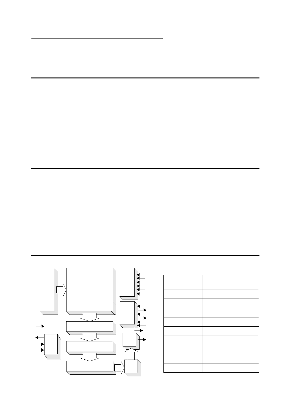
BLOCK DIAGRAM
DIGITAL
CONTROL
LOGIC.
ANALOG
VOLTAGE
5V
CKOUT
CKIN
SIN
VERTICAL
SHIFT
REGISTER
CLOCK
CIRCUIT
PHOTO DIODE ARRAY
Preliminar
COLUMN SENSE AMPLIFIERS
SAMP LE & H O LD
HORIZONTAL SHIFT REGISTER
REFS.
VIDEO
BUFFER
VIDEO
AMP
AGC
AEC
RESETB
LIN
BKLIT
CCIR
VRT
Vbloom
VOFF
VBG
EBCK
EVWT
2V7
AVO
Pixel Format 384 x 287 (CCIR)
320 x 243 (EIA)
Pixel Size 12µm x 12µm
Array Size 4.66mm x 3.54mm
Min. illumination 0.5 lux (Standard Clock)
S/N Typ ically 52dB
Exposure control Automatic (to 1460 00:1)
Gain Control Automatic (to +20dB)
Power Supply 5v ±5%
Power < 300 mW
Temperature 0
o
C - 40oC
cd27031c.fm 1
Page 2

VISION VV 5402 Sensor
MAIN FEATURES
Main Fe at ures 3
Specifications 5
Pin List 9
Video S ta ndards 12
Examp le Support Circ uit 15
Contents
page
eliminary
Pr
2 cd27031c.fm
Page 3

Main Features
Video Output
The VV5402 delive rs a fu lly -f ormatted
composit e m onochro m e v ideo signa l. S ta ndards optio ns include EIA (320 x 244) and
CCIR (384 x 287). On chip signal conditioning
allows user-select ion of linear or gam macorrected output.
The in tegra ted 75Ω driver eliminates the need
for additio nal active com ponents t o drive
standar d loads, inclu ding double t erminated
lines.
Automatic Exposure and Gain Control
Automa tic exposure and gain co nt rol are
enabled wi th AEC=1 (pin 21) and AGC = 1
(pin22). H ow ever, If AEC is inhibited by pin
21, AGC is als o inhibited . Inh ibiting AEC or
AGC by tak ing pin 21 or 22 low freeze s th e
current value(s) for th es e.
Automatic Gai n Con tr o l (AGC)
The VV5402 auto m at ic ally increas es t he
system gain of its output stage if with the
current gain setting and maximu m ex posure
the image is too dark. Gain can be varied from
x1 to x16 in times-two steps, giving five
different gain settings.
If the scene is too dark and the integration
period has almost reached its maximum
value, the gain valu e is inc remented by one
step (times two). In the same frame period the
exposure value is divided by two, halving the
integrat ion period. Th e exposure c ontroller
then inc reases the e xp os ure value as nec essary. Sim ilarly if the image is too bright and
the integration period is short then gain will be
reduced by one ste p (divide by two) and the
exposure value will be doubled. The exposure
controller can then adjust the exposure value
as nece s sa ry to provide a correctly exposed
image.
Automatic Exposure Control (AEC)
The VV5402 controls ex posure over a range
of 99,000 :1 in EIA mode and 146,00 0: 1 in
CCIR mode, and operates at illumination
levels as low as 0.5 lux at sta ndard clock
frequencies. (The syst em clock frequency can
be reduced to provide increased sensitivity.)
Automa tic exposure c ontrol is ach iev ed by
varying p ix el c urrent integration tim e
accordin g t o t he average light level on th e
sensor. T his int egration time can vary fro m
one pixel c loc k period to on e fr am e period.
reliminary
P
Pixels ab ov e a threshold white leve l are
counted ev ery f rame, and th e number at t he
end of the frame defines the image exposure.
If the image is other than correctly exposed, a
new value for integration time is calculated
and appli ed for the nex t frame. Corre c t ions
are either ±1/8 or ±1/64, depending upon the
degree o f over or under ex posure.
Backlit Mode
The VV5402 can b e c onf igured to o perate in
two auto-exposure modes, selected by the
BKLIT pin (pin28) stat e. The defa ult m ode
(BKLIT = 0) provides exposure control for
normally illuminated scenes . For scenes
where a bright back ground can ca us e the
foreground subje c t to be severely under
exposed, the ‘Backlit’ mode (BKLIT = 1) offers
superior performance.
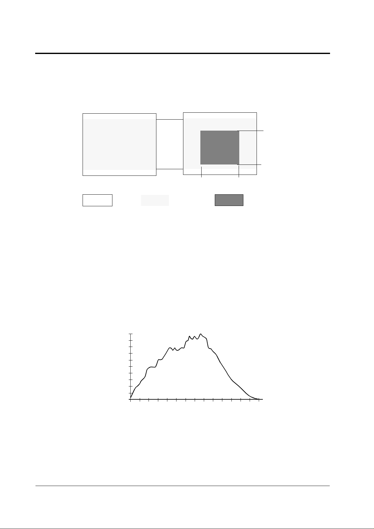
‘Backlit Mode’ (BKLIT=1) operates by using a
higher threshold level for the exposure control
comparator over the central area of an image,
which is t herefore exposed for longer and s o
enhan ce d. T he area in wh ic h t he higher
compa rat or threshold is used when BK LI T = 1
is illustrat ed below:
09/04/97 3
Page 4
VISION VV 5402 Sensor
Backlit Mode Threshold Area:
Normal operation (BKLIT=0) Higher threshold area (BKLIT=1)
10%
30%
80%
90%
25% 75%
Visible
image
Note: The threshold level used for the central area is a preset mutiple of the normal mode reference
level, and is not alterable.
Exposure
control area
25%
80%
Higher
Threshold
Spectral Resp onse
eliminary
1.0
0.8
Pr
0.6
0.4
0.2
Normalised Response
0
400
500
600
700
800
900
1000
Wavel ength nm
4 cd27031c.fm
1100
Page 5
SPECIFICATIONS
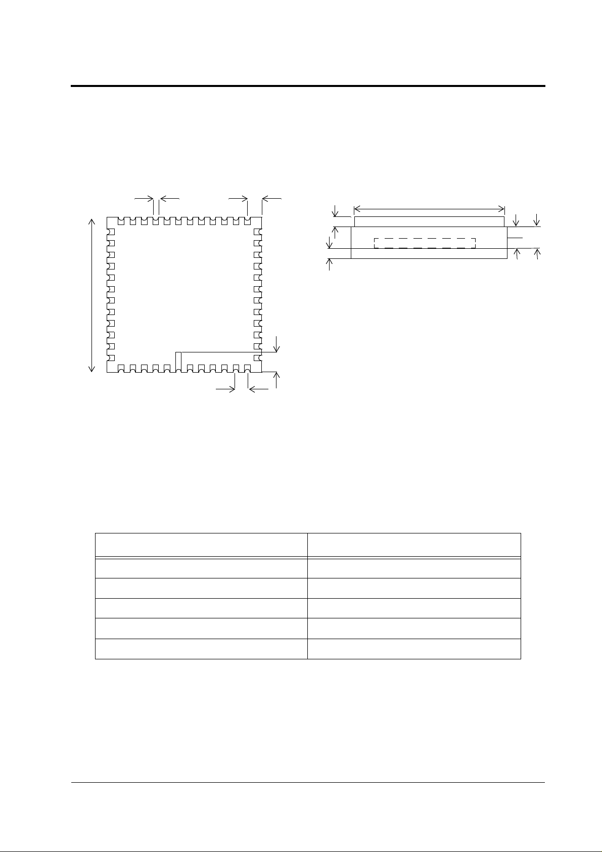
Package Details
Specifications
0.51
TYP
14.22
Viewed from below
1.52 TYP
2.16
PIN 1
1.016 PITCH TYP
13.7
0.55
0.53
The opti ca l array is centred within th e
package to a tolerance of ± 0.2 mm, and
rotated no more than ± 0.5
Toleranc es on pack age dimensions ±10%
Glass lid placement is controlled so that no
package overhang exists.
All dimens ions in millim etres
Glass Lid
Die
Base
Viewed from side
o
y
0.5
0.86
Absolute Ma x imu m Ra ti ngs
liminar
e
r
Parameter Val ue
P
Supply Voltage -0.5 to +7.0 volts
Voltage on other input pins -0.5 to V
Temperature under bias -15
Storage Temperature -30
Maximum DC TTL output Current Magnitude 10mA (per o/p, one at a time, 1sec. duration)
Note: Stresses exceeding the Absolute Maximum Ratings may induce failure. Exposure to absolute
maximum ratings for extended periods may reduce reliability . Functionality at or above these
conditions is not implied.
o
C to 85oC
o
C to 125oC
+ 0.5 volts
DD
09/04/97 5
Page 6

VISION VV 5402 Sensor
DC Operating Conditions
Symbol Parameter Min. Typ. Max. Uni ts Notes
V
DD
V
IH
V
IL
T
A
Operating supply voltage 4.75 5.0 5.25 Volts
Input Voltage Logic “1” 2.4 VDD+0.5 Volts
Input Voltage Logic “0” -0.5 0.8 Volts
Ambient Operating Temperature 0 70
AC Operating Conditions
Symb ol Par ameter Min. Typ. Max. Units No tes
CKIN
CKIN
1. Pixel Clock =
EIA Crystal frequency 12.0000 MHz 1
CCIR Crystal frequency 14.7456 MHz 1
CKIN
/
2
Electrical Characteristics
Symbol Parameter M in. Typ. Max. Units Notes
o
C S t ill air
I
DCC
I
ADD
I
DD
V
REF2V7
V
BG
V
OH
V
OL
I
ILK
1. Digital and Analogue outputs unloaded - add output current.
Digital supply current
Analog su pply current
Overall s upply current
Internal voltage reference 2.700 Volts
Internal bandgap reference 1.22 Volts
Output Voltage Logic “1” 2.4 Volts I
Output Voltage Logic “0” 0.6 Volts I
Input Le ak age curren t
Pr
eliminary
-1 µA
T ypical conditions, V
DD
10 mA 1
25 mA 1
35 mA 1
= 5.0 V, TA = 27oC
1 µA
= 2mA
OH
= -2mA
OL
VIH on
input
VIL on
input
6 cd27031c.fm
Page 7

Specifications
Operating Characterist ics
Parameter min. typ. max. units Note
Dark Current Signal 50 mV/Sec Modal pixel voltage due to photodiode leak-
age under zero illumination with Gain=1
= (Vt1 - Vt2)/(t1-t2), averaged over two
(V
dark
different frames)
Sensitivity 6 V/Lux·Sec V
Min. Illumination 0.5 Lux Standard CCIR clock
Shading TBA % Variance of V
Random Noise -52 dB RMS variance of all pixels, at 66% satura-
Smear TBA % Ratio of V
Flicker TBA % Variation of V
Lag TBA % Average residual signal with no illumination
Blooming TBA Ratio of spot illumination level that produces
liminar
/Lux·10ms, where Lux gives 50% satu-
Ave
ration with Gain=1 and Exposure=10ms
over eight equal blocks at
50% satu r ati o n lev e l illuminati on
tion, over four frames
25 lines high illuminated at 500xV
to V
Ave
at 66% saturation level illumination
in the field following one field of 66% sat.
illumina tion
0.1xV
sat
spot to the V
hole target)
ave
y
of the area outside a rectangle
ave
of the rectangle
of one line from field to field
ave
output from immediately around the
spot illumination level (pin-
sat
50%
level
e
Note: Devices are normaly not 100% tested for the above characterisation parameters, other than
Dark Current Signal (see Blemish Specification below).
All voltag e (
ishes are excluded (see Blemish Specification below). V
that is peak white.
VA, V
ave
, V
sat
, V
T est Conditions
The sensor is tested us ing the exam ple support
circuit illus t rat ed later in this document . Standard
imaging c onditions us ed for optica l te s ts employ a
tungsten halogen lam p to uniform ly illuminate the
sensor (to better than 0. 5%), or to illum inate
specific a reas. A neutr al density filte r is us ed to
control the level of llum ination where required .
09/04/97 7
r
P
) measurements are referenced to the black level, V
xx%
refers to the output that is xx% of saturation,
xx%
Illumination Colour T emp. 3200o K
Clock Frequency Std. CCIR
Exposure Maximum
Gain x1
Auto. Gain Control (AGC) Off
Correction mode Linear
, and spot blem-
black
Page 8
VISION VV 5402 Sensor
Blemish Specification
A Blemish is an area of pixels t hat produces output sig nif ic antly differe nt fro m it s su rrounding
pixels for the same illumination level. The definition of a Blemish Pixel varies according to testing
conditio ns as fo llows:
Test Exposur e Illumin ati o n Ble m is h Pi xe l o utput definitio n
1 - Black Frame Minimum Black Differing more than ± 100mV. from modal value.
2 - Dark Current Maximum Black Output more than three times the modal value
(see Dark Current Signal above).
3 - Pixel Variation Mid range 6 6% Sat. Differing more than ±35mV from modal value.
Note: The mode of pixel values must be within
±70 mV of 66% of V
Note: Gain is set to Minimum and Correction set to Linear for all tests; measurement of blemishes for
Test 3 is conducted under standard illumination (see above), set to produce average output of
66% saturation level.
for all dev ice s .
sat
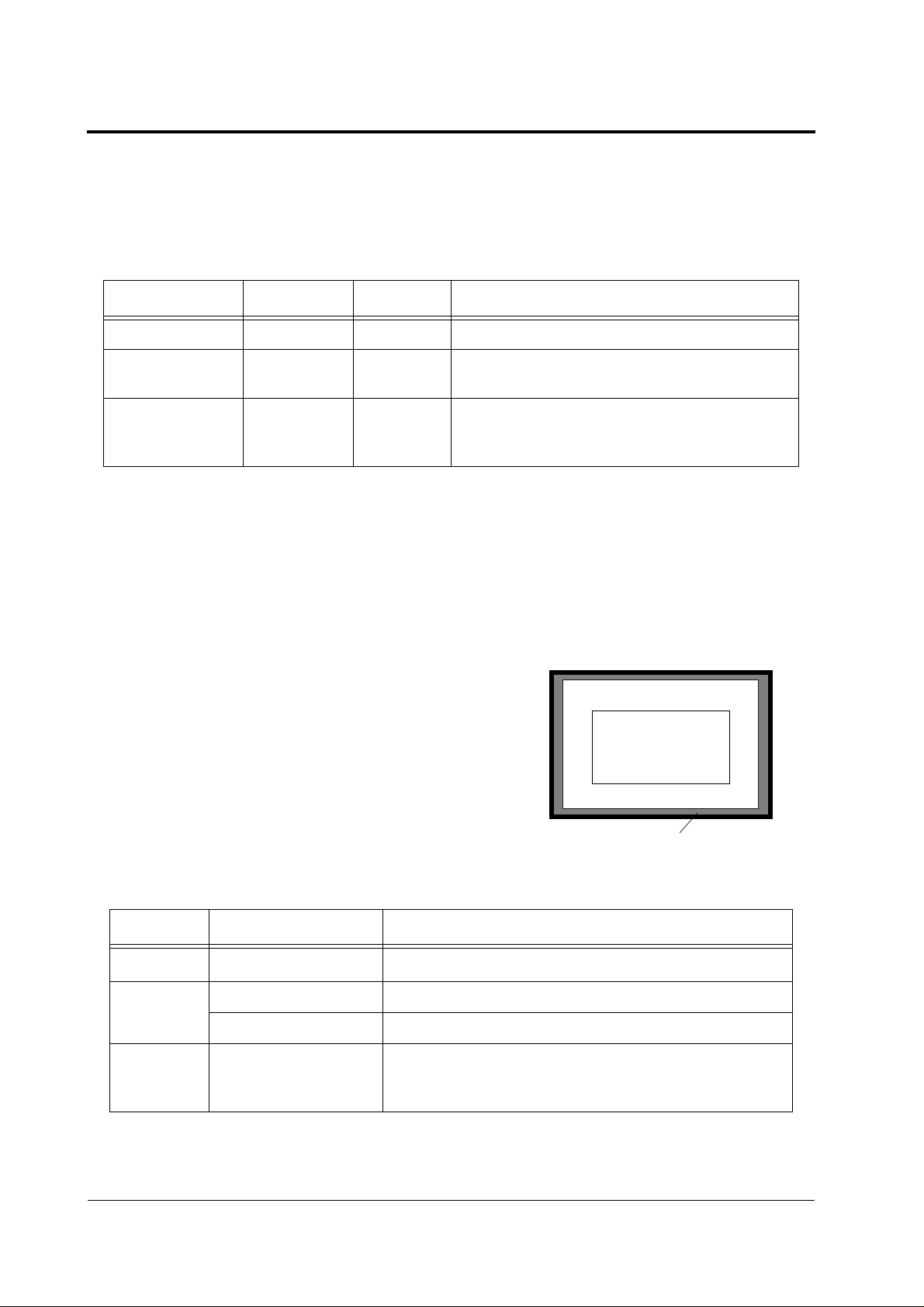
The pixel area of the sensor is divided into the following areas to qualify the blemish specification:
Area A is the central area of the array as defined
by the box w it h s ides 50% of t he linear height
and 50% of the linear width of th e array.
Area C is 10 vertical pixels by 10 horizontal pixels
around the edge of the array.
eliminary
Area B is the remain ing area of the array.
Area A
Area B
Area C
Pr
The blem is h s pecification is then def ined as follows :
Image Area Max. No. of Blemishes Notes
Area A 0 This is the most critical image area
4 Unconnected single pixels
Area B
Area C Any num ber Blemishes in this area are not significant, but the device
1 Of up to four connected pixels (2x2 max.)
shall, however, have no row or column (>50% of row or
column) faults in any area.
8 cd27031c.fm
Page 9
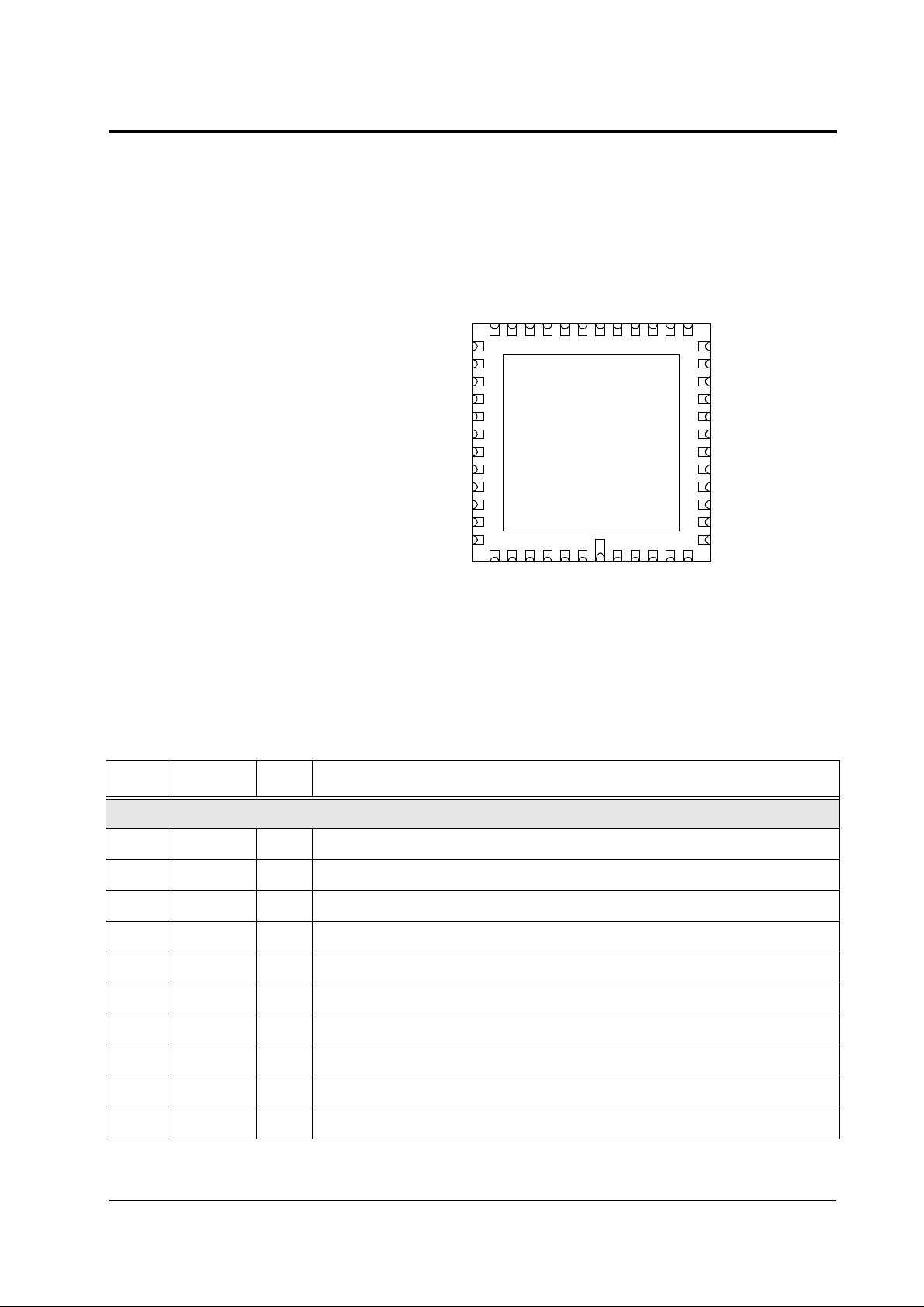
Pinout Diagram
48 Pin LCC
Viewed from top of packa ge
VSS
DNC
DNC
VDD
DNC
DNC
ODD
SCI
DNC
DNC
VDD
VSS
31
34
39
32
33
35
36
37
38
40
41
42
DNC
Pin List
CKOUT
CKIN
VDD
BKLIT
RESETB
24 23 22 21 20 1930 29 28 27 26 25
VSS
AGC
CCIR
y
LIN
AEC
SAB0
18
SCE
17
SIN
SAB1
16
15
VGND
14
AVO
13
VVDD
12
DNC
11
DNC
10
AVSS
9
EVWT
8
EBCK
7
AVDD
12345643 44 45 46 47 48
Pins Marked “DNC” must be left ‘floating’.
VRT
VBLWT
VCM
VBLOOM
VREF2V7
VBG
AVCC
AGND
PIN LIST
liminar
Pin Name Type Description
POWER SUPPLIES
1 AVCC PWR Core analogue power and reference supplies.
7 AVDD PWR output stage power. A VDD3 output stage logic.
10 AVSS GND Output stage ground. AVSS3 out p u t st age logic.
13 VVDD PWR 75ohm buffer supply.
15 VGND GND 75ohm buffer ground.
24,31 VSS GND Digital padring & logic ground.
P
e
r
VOFF/VPED
DNC
DEC2V2
DEC2V7
27,34 VDD PWR Digital padring & logic power.
41 DV DD PWR Core digital power.
42 DV S S GND Core digital ground.
48 A GND GND Core analogue ground and reference supplies.
09/04/97 9
Page 10

VISION VV 5402 Sensor
Pin Name Type Description
ANALOGUE VOLTAGE REFERENCES
2 VBG OA Internal bandgap reference voltage (1.22V nominal). Requires external
0.1uF capacitor.
3VOFF/
VPED
4 DEC2V2 OA Decouple 2.2V reference. Requires external 0.1uF capacitor.
5 DEC2V7 OA Decouple 2.7V reference. Requires external 0.1uF capacitor.
8 EBCK IA External black level bias. Internally generated. Decouple to VGND
9 EVWT IA External white pixel threshold for exposure control. Decouple to VGND
43 V B LWT IA Defines white level for clamp circuitry. Requires external 0.1uF capacitor.
44 VBLOOM OA Anti-blooming voltage reference. Requires external 0.1uF capacitor.
45 V RT IA Pixel reset voltage. Connect to VREF2V7 or external reference.
46 VCM IA Offset DAC common mode input. Connect to VREF2V7.
47 V RE F2V7 OA Internally generated 2.7V reference. Requires external 4.7uF capacitor.
ANALOGUE OUTPUTS
14 AVO OA Buffered Analogue video out. Can drive a doubly terminated 75ohm load.
SYSTEM CLOCKS
25 CKOUT OD Oscillator output. Connect Crystal for standard timing.
26 CKIN ID Oscillator input. Connect Cry stal f or standard ti mi ng.
IA Pedestal DAC & Offset Comp. DAC bias. Connect to VBG or external ref-
erence.
eliminary
IMAGE TIMING SIGNALS
37 ODD OD Odd/even field signal . (ODD = 1 for odd fields, ODD = 0 for even)
10 cd27031c.fm
Pr
Page 11

Pin List
Pin Name Type Description
DIGITAL CONTROL SIGNALS
16 SAB1 ID↓ Chip Address, Bit 1
17 SIN ID↓ Used to reset video timing control logic without resetting any other part of
VV5402. Resets video logic on the falling edge of the SIN pulse.
18 SCE ID↓ Scan Mode Enable - only relevant to test mode.
19 LIN ID↓ Gamma corrected or Linear output. LIN = 0, gamma corrected output,
LIN = 1, linear output. Default is gamma.
20 SAB0 ID↓ Chip Address, Bit 0
21 AEC ID↑ Automatic exposure control. AEC = 1, auto exposure is enabled; AEC = 0
auto exposure and auto gain control are disabled.
y
22 AGC ID↑ Automatic gain control enable. AGC = 1, auto-gain is enabled (if AEC = 1);
AGC = 0, auto-gain is disabled.
23 CCIR ID↑ Select default video mode for power-on. CCIR = 1 for CCIR video. EIA
video mode is selected when CCIR = 0. Default is CCIR if unconnected
28 BKLIT ID↓ Normal or Backlit exposure control mode. BKLIT = 0, normal mode; BKLIT
= 1, backlit mode. Default is normal. See Exposure Control for details.
29 RESETB ID↑ Active low camera reset. All camera systems are reset to power-on state.
38 SCI ID↓ S can Chain Input - only relevant to test mode.
liminar
OTHER PINS
e
6, 11, 12, 30, 32,
33, 35, 36, 39, 40
DNC DO NOT CONNECT. These pins must be left ‘floating’ for correct opera-
tion.
r
P
Key:
OA - Analogue output IA - Analogue input
OD - Digital output ID - Digital input
OD↓ - Digital out put with internal pull- down ID↑ - Digital input with internal pull-up
BI - Bidirectional DNC- Do Not Connect
09/04/97 11
Page 12
VISION VV 5402 Sensor
VIDEO STANDA RDS
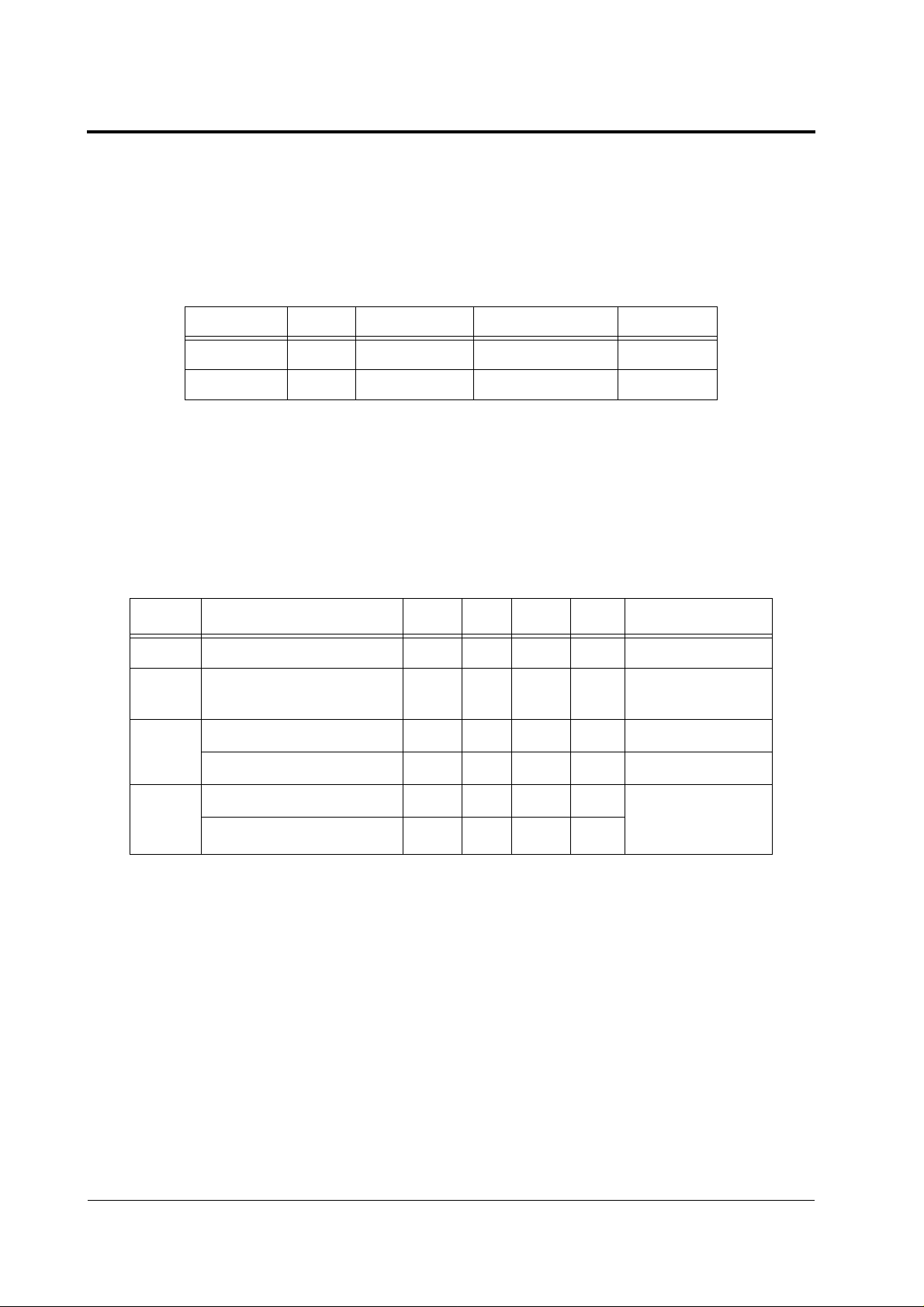
The VV5402 has 2 different video format modes, producing CCIR or EIA standard composite
Monoch rom e video ou tp ut . Line standards and frequ encies are as f ollows:
Video Mode Format Image (Pixels) Crystal Frequency CCIR pin
CCIR 4:3 384 x 287 14.7456 MHz 1
EIA 4:3 320 x 243 12.0000 MHz 0
VV5402 Video Modes
Video signal Characteristics
The following table summaris es th e c om posite video output lev els (AVO) for t he two standards,
which are graphically illustrated on the following pages:
Symbol Parameter Min. Typ. Max. Units Notes
V
V
V
V
Sync
blank
black
Sat
CCIR, EIA Sync. level
CCIR, EIA Blanking
level
CCIR Black level
EIA Blac k lev el
CCIR Saturation level
EIA Sat uration level
eliminary
0.3 V
0.9 V
0.9 V
1.0 V
2.3 V
2.4 V
DC reference
level
Peak Whi te ;
AVO clipped at
this level
Pr
Note: All measurements are made with AVO driving one 75Ω load.
12 cd27031c.fm
Page 13
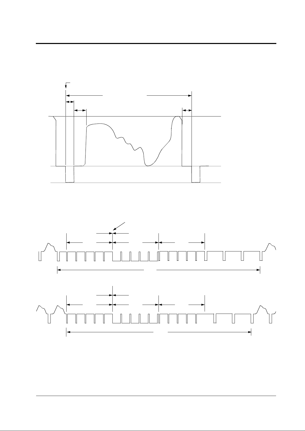
CCIR Timing Diagram
Video Standards
line time reference poin
line sync. 4.7µs
back porch 5.8µs
t
line period H = 64µs
front porch 1.5µs
peak white level
CCIR composite video signal - line level timing
frame start
rise times
(10% - 90%)
line blank 0.3 ± 0.1µs
{
line sync. 0.25 ± 0.05µs
2.3v
0.9v
y
0.3v
black &
blanking level
sync. level
field 0
2.5H 2.5H2.5H 2.5H
field 1
liminar
e
r
26H
P
field 1 field 2
2.5H 2.5H 2.5H
25H
CCIR composite video signal - field level timing
≈
≈
09/04/97 13
Page 14
VISION VV 5402 Sensor
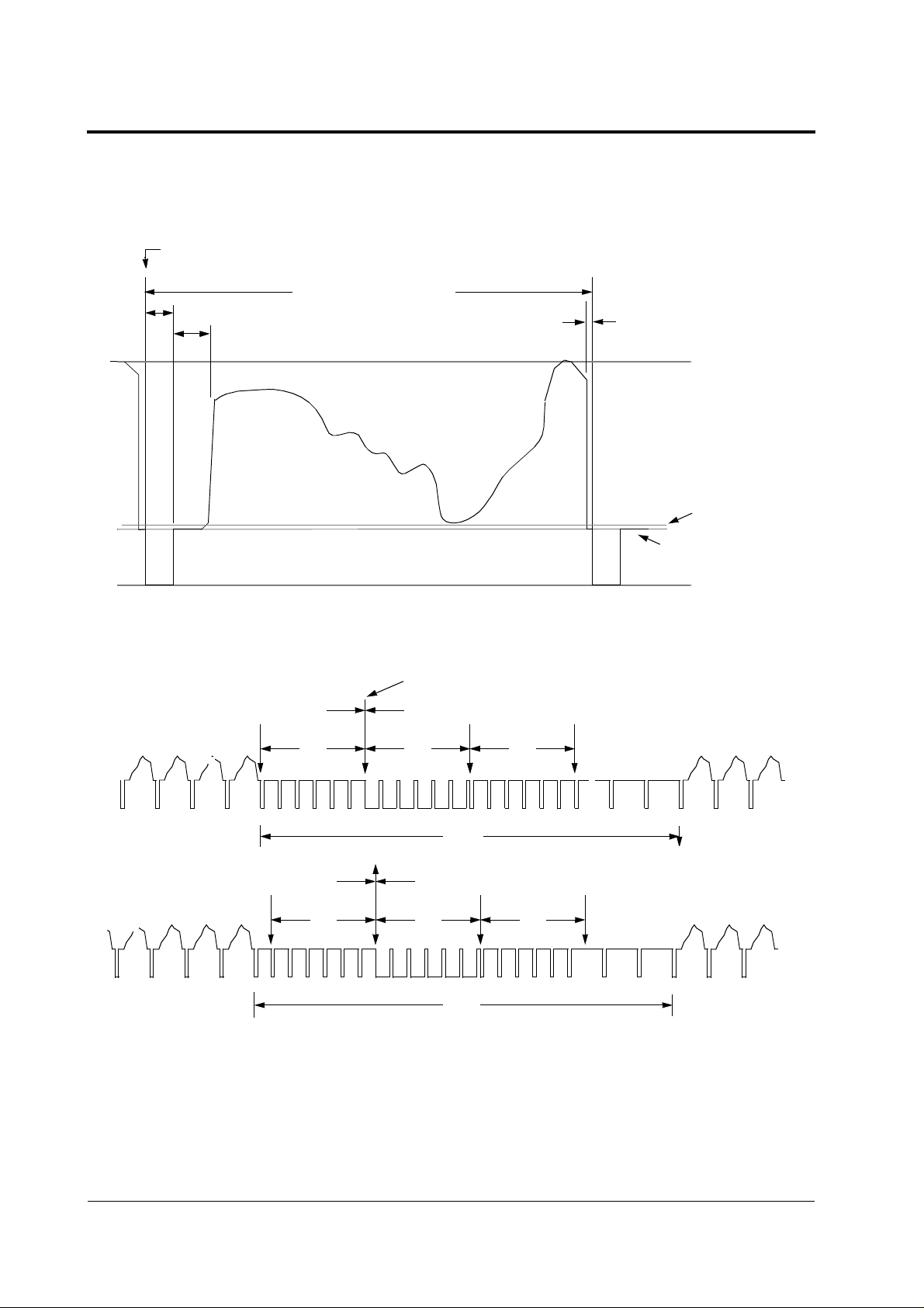
EIA Timing Diagrams
line time reference point
line sync. 4.83µs
back porch 4.00 µs
rise times
(10% - 90%)
line period H = 63.5µs
front porch 1.33µs
peak white level
EIA composite video signal - line level timing
frame start
line blank 0.3 ± 0.1µs
{
line sync. 0.25 ± 0.05µs
2.4v
0.9v
0.3v
black level
1.0v
blanking level
sync. level
≈
field 0 field 1
3H3H3H
≈
≈
eliminary
19H
Pr
field 1 field 2
3H3H3H
≈
20H
EIA composite video signal - field level timing
14 cd27031c.fm
Page 15
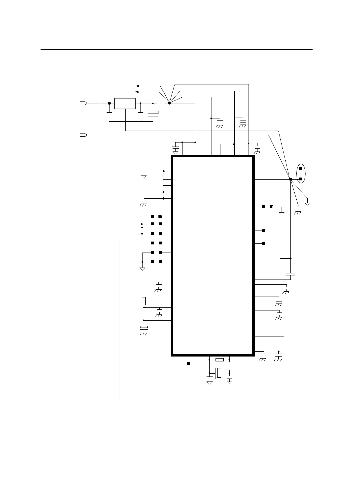
EXAMPLE SUPPORT CIRCUIT
AVD
VDD
8
+7 to +12v dc
0v
REG1
2,3,
C1
1
6,7
C2
Example Support Circuit
R1
C6C5
C3
1. Keep nodes Supply and Ground pins
low impedance and independent
2. Video output should be referred to VGND.
3. Keep circuit com ponents close to chip
pins (especially de-coupling capacitors)
VDD
Component Value
IC1 VV5402
REG1 LM78L05
C1,C2 0.22 µF
C3 68 µF
(6V Tant.)
C4-C9,C13, 0.1 µF
C16-C19
C10 4.7µF
C11, C12 10 pF
C14 100pF
R1 5R6
R2 10R
R3 10M
R4 75R
R5 33R
P
R5
r
C10
C4
34
27
VDD2VDD1
DVDD
24
VSS1
31
VSS2
42
DVSS
10
AVSS
48
AGND
16
SAB1
20
SAB0
28
BKLIT
19
LIN
22
AGC
21
AEC
44
liminar
C8
e
C9
45
46
47
VBLOOM
VRT
VCM
VREF2V7
(48 pin LCC)
VV5402
SIN
17
1
41
AVCC
IC1
CKIN CKOUT
26
R3
13
7
AVDD
VVDD
VGND
y
CCIR
EBCK
EVWT
VBLTW
DEC2V7
DEC2V2
VOFF/VPED
VBG
25
R2
AVO
SCI
SCE
C7
R4
14
15
23
38
18
C19
8
9
43
5
4
3
2
C13
MONITOR
C18
C17
C16
C15
C14
X1 Crystal
CCIR:14.7456 MHz
EIA:12.0000 MHz
Use Surface Mount components throughout.
09/04/97 15
C11
C12
X1
Page 16

VISION VV 5402 Sensor
VLSI VISION LIMITED
UK Office
Aviation House,
31 PInkhill,
Edinburgh, UK
EH12 7BF
Tel: +44 (0)131 539 7111
Fax: +44 (0)131 539 7140
Email: [email protected]
VLSI Visio n Lt d. res erv es the right to make changes to its pro ducts and specifications at any time. Information furnished by VISION is believed to be accurate, but no responsibility is ass um ed by VISION fo r t he use of said inf ormation, nor a ny inf ringemen ts of patents or of any other t hird party right s w hic h
may result f rom s aid use. No lice ns e is granted by implicati on or otherwis e
under an y pat ent or patent rights of any VI SION group co m pany.
VLSI Vision agent or distributor
USA West Office
18805 Cox Avenue,
Suite 260,
Saratoga,
California 95070, USA
Tel: +1 408 374 5323
Fax: +1 408 374 4722
Email: [email protected]
© Copyrigh t 1996, VLSI VI SI ON
USA East Office
2517 Highway 35
Bldg F, Suite 202
Manasquan
New Jersey 08736
Tel: +1 908 528 2222
Fax: +1 908 528 9305
Email: [email protected]
eliminary
Pr
16 cd27031c.fm
 Loading...