

Datasheet VV6301B001, VV0670P001, VV5301B001, STV-6301-R01, STV-6301-E01 Datasheet (Vision)
...Page 1

V:\apps\cpia\docs\cpia datasheet\cpia_datasheet4.fm
02/07/98
VISION
CPiA Data Sheet (VV0670P001)
Colour Processor Interface ASIC
Commercial In Confidence
Revision Histor
y
REV Change Revised b
y
Date
1Ori
g
inal Document Ed Duncan 4/12/97
2First Bod
y
Text Added Peter Slawek 09/02/98
3 Amendments & added prelim VP section Ed Duncan 12/02/98
4 Restructure and add DRAM timin
g
Ed Duncan 26/03/98
5 Substantiated - more sections, text and dia
g
rams Ed Duncan 01/03/98
6 Power mana
g
ement + compression + mech drawings Ed Duncan 03/03/98
7 Add REM’s parallel port section Ed Duncan 10/04/98
8 Extended CP section REM 13/04/98
9 Add USB section and proof read document Linda Russell 02/07/98
Page 2
V:\apps\cpia\docs\cpia datasheet\cpia_datasheet4.fm
02/07/98 2
Commercial In Confidence
T
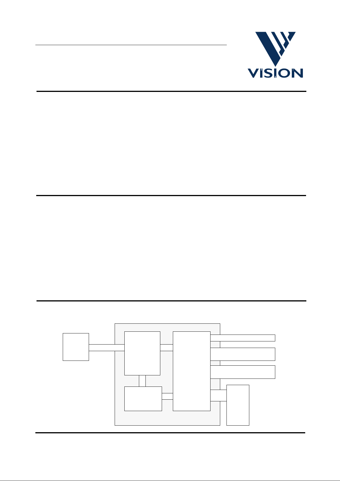
he Colour Processor Interface ASIC (CPiA) is a
di
g
ital video processor requiring only a single
4Mbit DRAM and minimum of passive support
components to provide a complete PC peripheral
video capture s
y
stem.
CPiA accepts raw di
g
ital video data from Vision’s
CIF format CMOS sensors and is capable of
transferrin
g
the resulting YUV video data to a hos t
PC over either USB or Parallel Port interfaces at
rates up to 30 frames per second.
The CPiA architecture consists of three
conceptuall
y
separate functional blocks: the Video
Processor
(VP)
, the Video Compressor (VC) and
the Control Processor
(CP)
.
The VP controls the VVL404 sensor and
processes the raw pixel data into CIF or QCIF
YUV ima
g
es for compression and transfer to the
Host b
y
the VC.
The CP is responsible for coordinatin
g sy
stem
operation, respondin
g
to host requests and
commands as well as perfor min
g
automatic camera
exposure control and colour balance.
• Interfaces to Vision’s VV6404 colour CMOS
ima
g
e sensor
•Directl
y
interfaces to a host PC using USB or
Parallel port interfaces
• 100% compliant with USB specification v1.0
• 100% compliant with IEEE1284 parallel port
specifications
• Support for Windows 95/98 Plu
g
and Pla
y
•Image capture at CIF (352x288) and
QCIF
(
176x144) resolutions
•Ima
g
e compression providing up to 30fps CIF
• Automatic exposure control and co lour balance
• Camera flicker control for 50 Hz and 60 Hz
mains driven li
g
htin
g
• Supports selective transfer of requested
re
g
ions of interest to the host system
• Power mana
g
ement including watchdog reset
• Absolute minimum of support components
• Device pinout desi
g
ned to facilitate layout and
area of support PCB
CPiA SYSTEM BLOCK DIAGRAM
GENERAL DESCRIPTION
Colour Processor Interface ASIC
VISION CPiA
DATASHEET
FEATURES
CPiA
VP
VC
CP
VVL404
Ima
g
e
Sensor
DRAM
USB
PP
(
host
)
PP(pass
)
Page 3
V:\apps\cpia\docs\cpia datasheet\cpia_datasheet4.fm
02/07/98 3
Colour Processor Interface ASIC
Commercial In Confidence
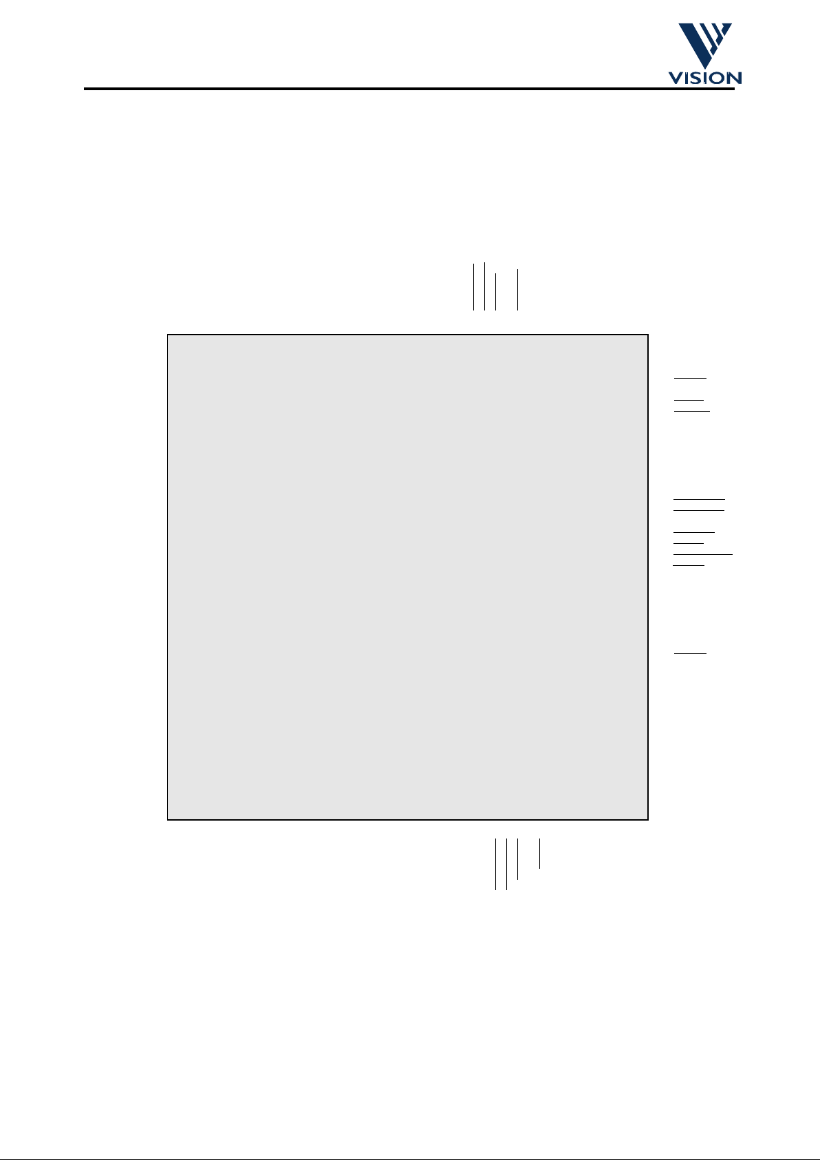
1.1 Representative Device Pinout
CPiA has been packaged in an industry-standard 176 TQFP. The pinout has been carefully developed to
minimise the ph
y
sical size of the support printed circuit board by facilitating placement of and electrical
routin
g
to peripheral support components such as DRAM and parallel port connectors.
Reference should also be made to drawin
g
s located at the end of this data sheet for physical dimensions and
other, more detailed mechanical information.
132 NC
131 NC
130 RAMA[4]
129 RAMA[3]
128 RESET
127 CLK400H
126 NORM
125 LOPOW
124 VSS
123 VSS
122 CKO14
121 CKI14
120 CKO48
119 CKI48
118 VDD
117 P_STROBE
116 P_AUTOFD
115 VSS
114 P_FAULT
113 P_INIT
112 P_SELECTIN
111 P_ACK
110 P_BUSY
109 P_PERROR
108 P_SELECT
107 H_SELECT
106 H_PERROR
105 VSS
104 H_BUSY
103 H_ACK
102 VDD
101 VSS
100 VSS
99 VDD
98 HP_DATA[7]
97 VSS
96 HP_DATA[6]
95 HP_DATA[5]
94 VSS
93 HP_DATA[4]
92 VDD
91 HP_DATA[3]
90 NC
89 NC
176 TQFP
176 NC
175 NC
174 NC
173 VDD
172 VSS
171 VSS
170 VSS
169 VSS
168 RAMD[15 ]
167 RAMD[0]
166 RAMD[14 ]
165 VSS
164 RAMD[1]
163 RAMD[13 ]
162 RAMD[2]
161 RAMD[12 ]
160 RAMD[3]
159 RAMD[11]
158 VSS
157 RAMD[4]
156 RAMD[10 ]
155 RAMD[5]
154 VDD
153 RAMD[9]
152 RAMD[6]
151 VSS
150 RAMD[8]
149 RAMD[7]
148 RAMLCAS
147 RAMUCAS
146 RAMWE
145 VSS
144 RAMRAS
143 RAMA[8]
142 RAMA[7]
141 RAMA[0]
140 VDD
139 RAMA[6]
138 RAMA[1]
137 RAMA[5]
136 VSS
135 RAMA[2]
134 NC
133 NC
NC 1
NC 2
NC 3
VDDA 4
SCLK 5
VSS 6
SDATA[0] 7
SDATA[1] 8
SDATA[2] 9
SDATA[3] 10
SSDA 11
SSCL 12
VDDA 13
VDDA 14
VSS 15
DC 16
DC 17
DC 18
DC 19
DC 20
DC 21
VSS 22
DC 23
DC 24
DC 25
VDDA 26
DC 27
DC 28
DC 29
DC 30
DC 31
VSS 32
DC 33
DC 34
DC 35
DC 36
DC 37
DC 38
DC 39
DC 40
DC 41
NC 42
NC 43
NC 44
NC 45
NC 46
DC 47
DC 48
DC 49
DEBUG 50
ID_SELECT 51
USB_BANDWIDTH 52
RXD 53
VSS 54
TXD 55
SPARE0 56
SPARE1 57
SPARE2 58
VSS 59
DC 60
DC 61
DC 62
DC 63
VSS 64
DC 65
DC 66
DC 67
DC 68
VDDA 69
VSSU 70
DP 71
DN 72
VDDU 73
VDD 74
H_STROBE
75
H_AUTOFD
76
H_FAULT
77
VSS 78
H_INIT
79
H_SELECTIN 80
HP_DATA[0] 81
VSS 82
HP_DATA[1] 83
HP_DATA[2] 84
VSS 85
NC 86
NC 87
NC 88
CPiA
Page 4
V:\apps\cpia\docs\cpia datasheet\cpia_datasheet4.fm
02/07/98 4
Colour Processor Interface ASIC
Commercial In Confidence
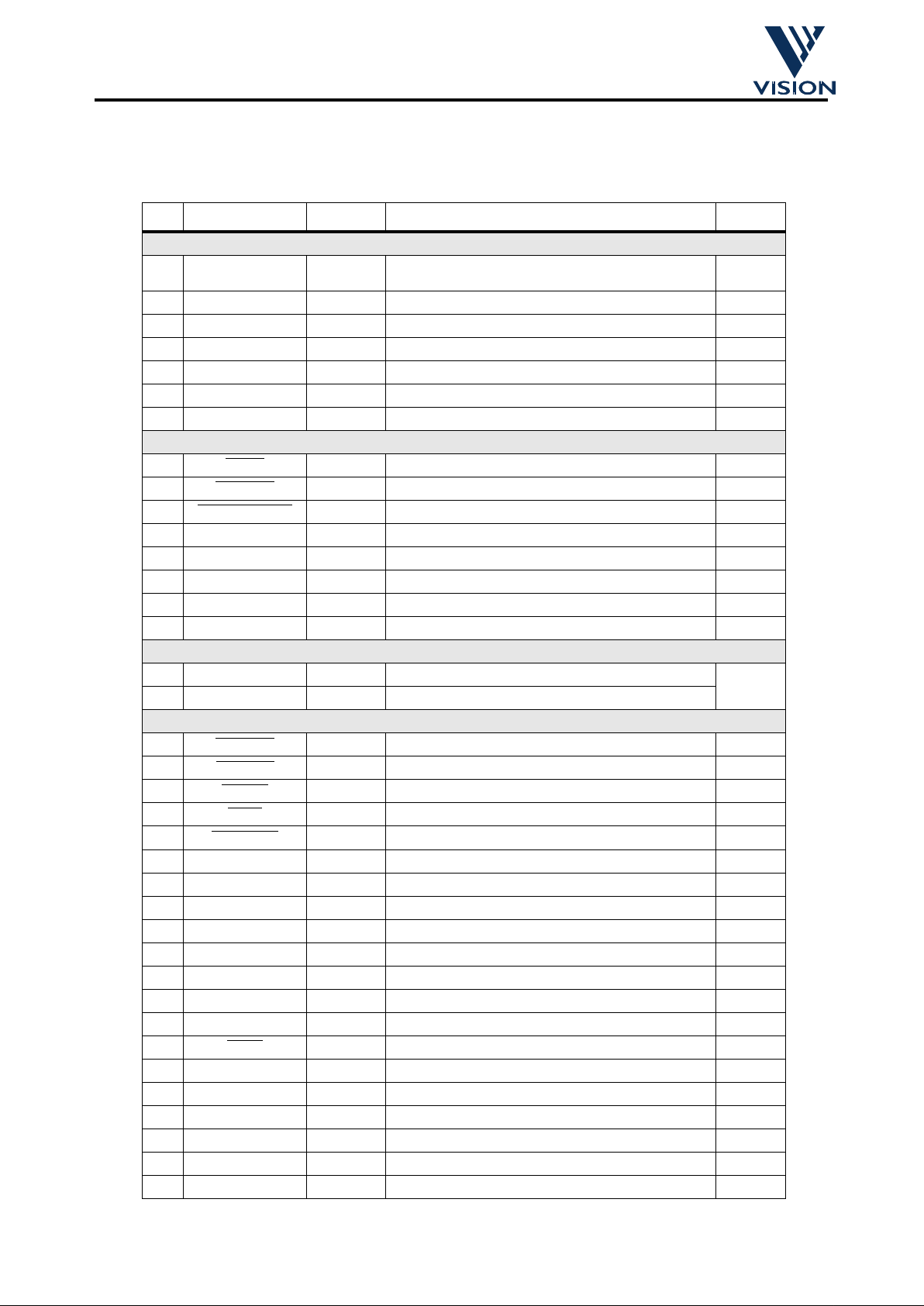
1.2 CPiA Pin Description
1.2.1 Device I/O
Pin Signal Type Description drive
Video Processor
5 SCLK O (4) VVL6404 Sensor Clock (7.159MHz) 2 mA
or 4mA
7 SDATA[0] I (3) VVL6404 Sensor Data Bus 8 SDATA[1] I (3) VVL6404 Sensor Data Bus 9 SDATA[2] I (3) VVL6404 Sensor Data Bus -
10 SDATA[3] I (3) VVL6404 Sensor Dat a Bus 11 SSDA I/O (2,3,6) VVL6404 Sensor Serial Interface Data 2 mA
12 SSCL I/O (2,3,6) VVL6404 Sensor Serial Interface Clock 2 mA
Control Processor
50 DEBUG I Control Processor Debug Output Select 51 ID_SELECT
I DUAL Camera Device ID Select -
52 USB_BANDWIDTH
I Alternate USB Bandwith Settings 53 RXD I Control Processor Serial Communications 55 TXD O(4,6) Control Processor Serial Communications 2 mA
56 SPARE0 I Control Processor spare (P1.1) 57 SPARE1 I Control Processor spare (P3.4) 2 mA
58 SPARE2 I Control Processor spare (P3.5) 2 mA
USB
71 DP I/O (1,5,7) USB Differential Output (+) 72 DN I/O (1,5,7) USB Differential Output (-) -
Parallel Port Interface
75 H_STROBE I (1,4,9) Parallel port HOST STROBE control 76 H_AUTOFD
I (1,4,9) Parallel port HOST AUTOFEED control -
77 H_FAULT
O (5,9) Parallel port HOST FAULT status 16 mA
79 H_INIT
I (1,4,9) Parallel port HOST INIT control -
80 H_SELECTIN
I (1,4,9) Parallel port HOST SELECTIN control 81 HP_DATA[0] I/O (1,4,5,9) Parallel port Host/Pass data bus 16 mA
83 HP_DATA[1] I/O (1,4,5,9) Parallel port Host/Pass data bus 16 mA
84 HP_DATA[2] I/O (1,4,5,9) Parallel port Host/Pass data bus 16 mA
91 HP_DATA[3] I/O (1,4,5,9) Parallel port Host/Pass data bus 16 mA
93 HP_DATA[4] I/O (1,4,5,9) Parallel port Host/Pass data bus 16 mA
95 HP_DATA[5] I/O (1,4,5,9) Parallel port Host/Pass data bus 16 mA
96 HP_DATA[6] I/O (1,4,5,9) Parallel port Host/Pass data bus 16 mA
98 HP_DATA[7] I/O (1,4,5,9) Parallel port Host/Pass data bus 16 mA
103 H_ACK
O (5,9) Parallel port HOST ACK status 16 mA
104 H_BUSY O (5,9) Parallel port HOST BUSY status 16 mA
106 H_PERROR O (5,9) Parallel port HOST PERROR status 16 mA
107 H_SELECT O (5,9) Parallel port HOST SELECT status 16 mA
108 P_SELECT I (1, 4,9) Parallel port PASS-THRU SELECT status 109 P_PERROR I (1,4,9) Parallel port PASS-THRU PERROR status 110 P_BUSY I (1,4,9) Parallel port PASS-THRU BUSY status -
Page 5
V:\apps\cpia\docs\cpia datasheet\cpia_datasheet4.fm
02/07/98 5
Colour Processor Interface ASIC
Commercial In Confidence
111 P_ACK I (1,4,9) Parallel port PASS-THRU ACK status 112 P_SELECTIN
O (5,9) Parallel port PASS-THRU SELECTIN control 16 mA
113 P_INIT
O (5,9) Parallel port PASS-THRU INIT control 16 mA
114 P_FAULT
I (1,4,9) Parallel port PASS-THRU FAULT status -
116 P_AUTOFD
O (1,5,9) Parallel port PASS-THRU AUTOFEED control 16 mA
117 P_STROBE
O (1,5,9) Parallel port PASS-THRU STROBE control 16 mA
VC Master Clocks
119 CKI48 I(8) 48.0MHz Oscillator Amplifier Input Pad 120 CKO48 O(7) 48.0MHz Oscillator Amplifier Output Pad
121 CKI14 I 14.318MHz Oscillator Amplifier Input Pad 122 CKO14 O 14.318MHz Oscillator Amplifier Output Pad
Power Management Inte rfa ce
125 LOPOW O(7) External device VCC control 2 mA
126 NORM
O(7) External device VCC control 2 mA
127 CLK400H I (4) Power management clock 128 RESET
I (4) Master Reset -
System Memory (DRAM) Interface
129 RAMA[3] O (10) DRAM multiplexed address 2 mA
130 RAMA[4] O (10) DRAM multiplexed address 2 mA
135 RAMA[2] O (10) DRAM multiplexed address 2 mA
137 RAMA[5] O (10) DRAM multiplexed address 2 mA
138 RAMA[1] O (10) DRAM multiplexed address 2 mA
139 RAMA[6] O (10) DRAM multiplexed address 2 mA
141 RAMA[0] O (10) DRAM multiplexed address 2 mA
142 RAMA[7] O (10) DRAM multiplexed address 2 mA
143 RAMA[8] O (10) DRAM multiplexed address 2 mA
144 RAMRAS_n O (10) DRAM row address strobe 8 mA
146 RAMWE_n O (10) DRAM data write enable 2 mA
147 RAMUCAS_n O (10) DRAM upper column address strobe 8 mA
148 RAMLCAS_n O (10) DRAM lower column address strobe 8 mA
149 RAMD[7] I/O (10) DRAM data 2 mA
150 RAMD[8] I/O (10) DRAM data 2 mA
152 RAMD[6] I/O (10) DRAM data 2 mA
153 RAMD[9] I/O (10) DRAM data 2 mA
155 RAMD[5] I/O (10) DRAM data 2 mA
156 RAMD[10] I/O (10) DRAM data 2 mA
157 RAMD[4] I/O (10) DRAM data 2 mA
159 RAMD[11] I/O (10) DRAM data 2 mA
160 RAMD[3] I/O (10) DRAM data 2 mA
161 RAMD[12] I/O (10) DRAM data 2 mA
162 RAMD[2] I/O (10) DRAM data 2 mA
163 RAMD[13] I/O (10) DRAM data 2 mA
164 RAMD[1] I/O (10) DRAM data 2 mA
166 RAMD[14] I/O (10) DRAM data 2 mA
167 RAMD[0] I/O (10) DRAM data 2 mA
Pin Signal Type Description drive
Page 6

V:\apps\cpia\docs\cpia datasheet\cpia_datasheet4.fm
02/07/98 6
Colour Processor Interface ASIC
Commercial In Confidence
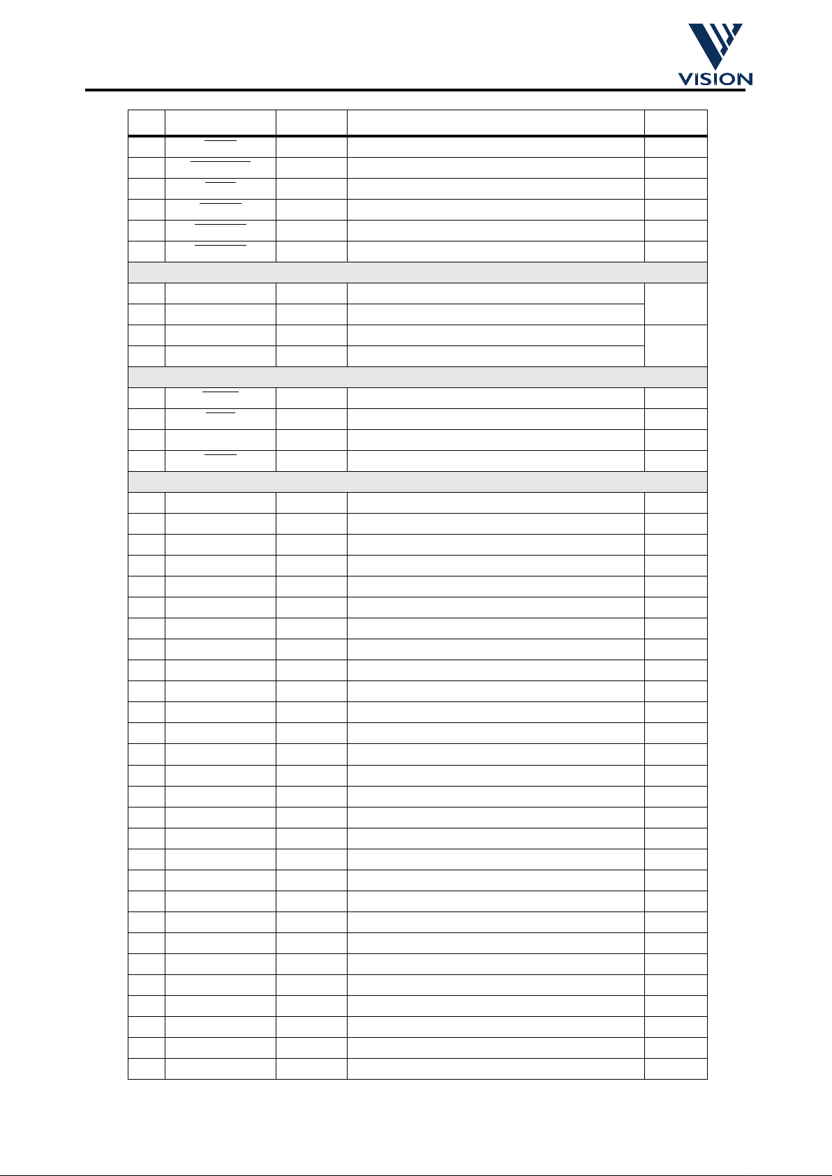
If the target application requires that only one interface mode is required (eg. USB interface only), please
refer to the above tab le and note s 7, 8 and 9 to establis h how unus ed pins sh ould be el ectricall
y
connected
on the PCB. Failure to ensure such pins are correctl
y
connected may result in erroneous system behaviour.
Notes:
1. Internal pullups.
2. These pins shall
g
o tri-state when LOPOW is high.
3. TTL level Schmitt input.
V
IL(max)
= 0.8V, V
IH (MIN)
= 2.2V, schmitt trigger hysteresis=250mV (typ).
Input leaka
g
e -10µA to +10µA, VIN : 0 to DVDD
4. Output
V
OL(max)
=0.4V @ IOL =16mA
V
OH(min)
=2.4V @ IOH = -12mA
5. These si
g
nals to comply with USB Specification Version 1.0 section 7.
6. Open drain output.
V
OL(max)
=0.4V @ IOL =3mA
7. This pin does not re
q
uire connection if CPiA is used for parallel port interfacing products only.
8. This pin should be tied low if CPiA is used for parallel port interfacin
g
products only.
9. This pin does not re
q
uire connection if CPiA is used for USB interfacing products only.
10. These pins shall
g
o tri-state when NORM is high.
Where I/O pad t
y
pe is not explicitly defined in the above notes assume CMOS.
168 RAMD[15] I/O (10) DRAM data 2 mA
Pin Signal Type Description drive
Page 7
V:\apps\cpia\docs\cpia datasheet\cpia_datasheet4.fm
02/07/98 7
Colour Processor Interface ASIC
Commercial In Confidence
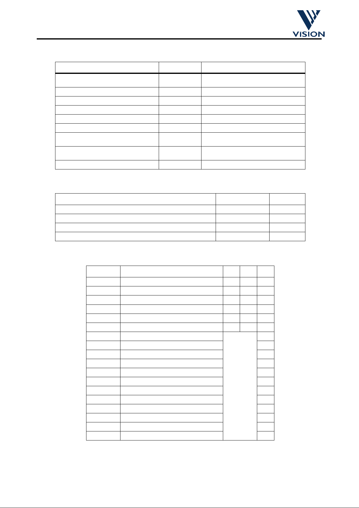
1.2.2 Device Power, NC and DC pins
1.3 Absolute Max Ratings
1.4 DC Characteristics
Pin Signal Description
6, 15, 22, 32, 54, 64, 78, 82, 85, 94, 100, 101, 105,
115, 124, 136, 145, 151, 158, 165, 97
VSS Digital padring & logic ground.
59, 123, 169, 170, 171, 172 VSS Reserved Signal Inputs (Tie Low)
4, 13, 14, 26, 69 VDDA Digital padring & logic power for VP & CP
74, 92, 99, 102, 118, 140, 154, 173 VDD Digital padring & logic power for VC
70 VSSU Ground for the USB
73 VDDU 3.3V supply for the USB
16, 17, 18, 19, 20, 21, 23, 24, 25, 27, 28, 29 , 30, 31,
33, 34, 35,36, 37, 38, 39, 40, 41, 47, 48, 49
DC Do NOT connect these pins
1, 2, 3, 42, 43, 44, 45, 46, 86, 87, 88, 89, 90, 131, 132,
133, 134, 174, 175, 176
NC Not connected pins
60, 61, 62, 63, 65, 66, 67, 68 DC Do NOT connect these pins
Description Range Unit
Ambient Temperature 0 to 40
o
C
Storage Temperature -50 to 150
o
C
Voltage on USB D+/D-, Vcc3V to Vss V
Voltage on any other I/O to Vss V
Parameter Description Min Max Units
VDD Primary CPiA Power Supply V
VDDA Secondary CPiA Power Supply V
VDDU 3.3V Power Supply for on-chip USB tranceiver V
Isuspend CPiA suspend mode current uA
Ilowpo CPiA low power modecurrent mA
Iactive CPiA active, high power mode current mA
Vilu, Vihu USB differential pad D+/D- Vil, Vih
See Section 1.2
V
Volu, Vohu USB differential pad D+/D- Vol, V oh V
Iilu, Iihu USB differential pad D+/D- Iil, Ili mA
Vilp, Vihp Parallel Port pads Vil, Vih V
Volp, Vohp Parallel Port pads Vol, Voh V
Iilp, Iihp Parallel Port pads Iil, Ili mA
Vild, Vihd Dram Interface pads Vil, Vih V
Vold, Vohd Dram Interface pads Vol, Voh V
Iild, Iihd Dram Interface pads Iil, Ili mA
Vilm, Vihm Power Management pads Vil, Vih V
Volm, Vohm Power Management pads Vol, Voh V
Iilm, Iihm Power Management pads Iil, Ili mA
Page 8
V:\apps\cpia\docs\cpia datasheet\cpia_datasheet4.fm
02/07/98 8
Colour Processor Interface ASIC
Commercial In Confidence
2 CPiA Functional Description
2.1 Video Processor Module
The CPiA video processor module provides CIF-format 4:2:2-sampled digital video to the VC module at frame
rates up to 30 frames per second and also interfaces directl
y
to the 356 x 292 pixel colour CMOS image sensor
provided in Vision’s VM6404 camera head module. Usin
g
a 9-wire cable and an absolute minimum of external
components, the interface incorporates:
1. A 4-wire data bus SDATA[3:0] for receivin
g
both video data and embedded timing references.
2. A 2-wire serial interface SSDA,SSCL for controllin
g
the camera.
3. The clock for camera module SCLK.
4. 5V and 0V power lines. CPiA is not re
q
uired to provide power directly to the camera; camera power is
derived from the s
y
stem power supply.
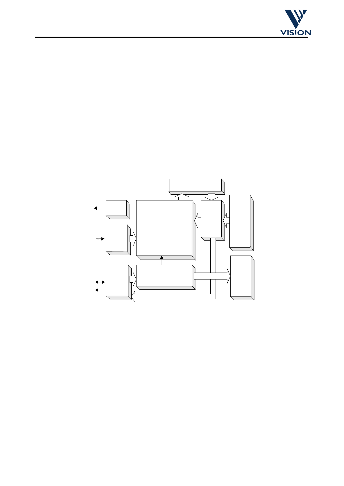
The simplified block dia
g
ram shown below highlights the key functional blocks within CPiA’s VP module.
CPiA provides a master clock SCLK to the camera module. Each 8-bit pixel value
g
enerated by the camera is
transmitted across the 4 wire databus SDATA[3:0] as a pair of se
q
uential 4-bit nibbles, most significant nibble
first. Codes representin
g
the start and end frames and the start and end of lines are embedded within the video
pixel data stream to allow the receiver to s
y
nchronise with the video data which the camera module is
g
enerating.
The video processin
g
engine performs these basic functions on incoming data: full colour restoration at each
pixel site from Ba
y
er-patterned input data, mat rixing/gain on each colour ch annel for colou r purity, aperture
correction for ima
g
e clarity, gamma correction, a nd colour space conv ersion (including hue and saturation
control
)
from RGB to YCbCr.
Ima
g
e statistic monitors gather data required by the CP module for end-of-frame housekeeping tasks such as
exposure control and colour balance.
The 2-wire camera serial interface provides complete control over how the sensor is setup and run.
COLOUR VIDEO
REGISTERS
SSDA
SSCL
SDATA[3:0]
RECEIVER
SCLK
CLOCK &
CONTROL
PIXEL DEFECT
ENGINE
SERIAL
INTER-
FACE
MONITORS
CORRECTION
CP CONTROL
INTERFACE
VC VIDEO DATA
INTERFACE
Block Diagram of CPiA Video Processor Module
Page 9
V:\apps\cpia\docs\cpia datasheet\cpia_datasheet4.fm
02/07/98 9
Colour Processor Interface ASIC
Commercial In Confidence
Camera exposure and gain values are programmed via this interface.
The followin
g
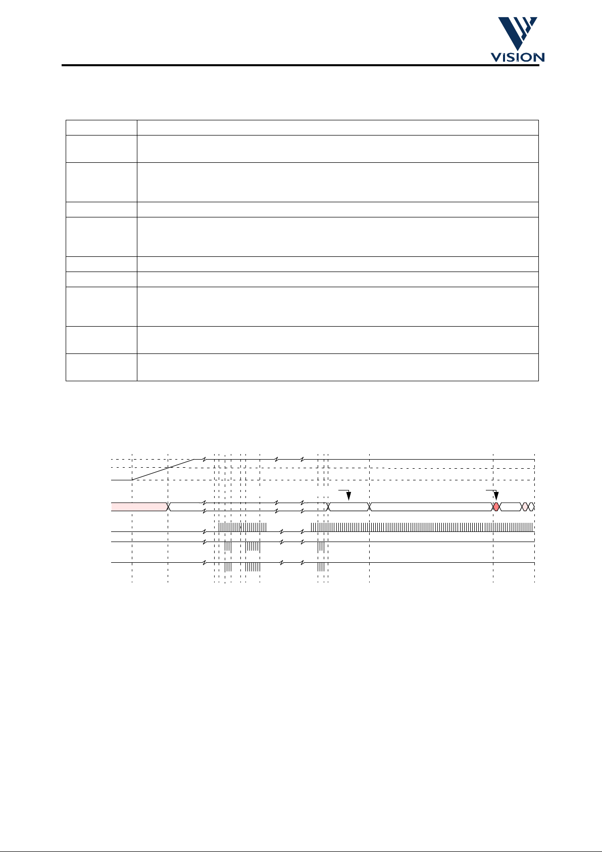
table and diagram illustrate the camera power up sequence.
PU0 S
y
stem Power Up
PU1 Sensor Internal-on Reset Tri
gg
ers, the sensor enters low power mode and
SDATA[3:0] is set to F
H
.
PU2 CPiA internall
y
releases video processing modules from reset. NOTE - this event is
under the control of the Control Processor, and does not occur until the host has
re
q
uested video from the camera.
PU3 CPiA enables the sensor clock, SCLK.
PU4-PU5 At least 16 SCLK clock periods after SCLK has been enabled CPiA sends a “Soft-
Reset” command to th e sensor via the serial interfac e. This ensures that if a sensor
is present then it is in low-power mode.
PU6 On detectin
g
32 consecutive FH values on SDATA [3:0], CPiA detects the camera
PU7-PU8 If present, CPiA uploads the sensor defect map from camera head E
2
PROM.
PU13-PU4 At least 16 SCLK clock periods after SCLK has been enabled, CPiA sends an “Exit
Low-Power Mode” command to the sensor via the serial interface. This initiates the
sensors 4 frame start se
q
uence.
PU15-PU16 One frame of alternati n
g
9H & 6H data on SDATA[3:0] fo r the CPiA to determine the
best samplin
g
phase for the nibble data SDATA[3:0].
PU17-PU18 4 Frames after the “Exit Low-Power Mode” serial comms, the sensor starts to output valid
video data.
F
H
F
H
5V
0V
2.8V
9H,6H,9H,6H...
Regulated
Sensor
Power
SDATA[3:0]
SCLK
SSDA
SSCL
PU0
PU1
PU3
PU2
PU4
PU5
PU6
PU7
PU8
Start of Frame Line for
the 1st frame of valid
One frame of 9H & 6H data.
PU13
PU14
PU15
PU16
PU17
PU18
Camera Head Interface Behaviour up to and including first valid video data
Page 10
V:\apps\cpia\docs\cpia datasheet\cpia_datasheet4.fm
02/07/98 10
Colour Processor Interface ASIC
Commercial In Confidence
2.2 Video Compressor Module
2.2.1 Power Management
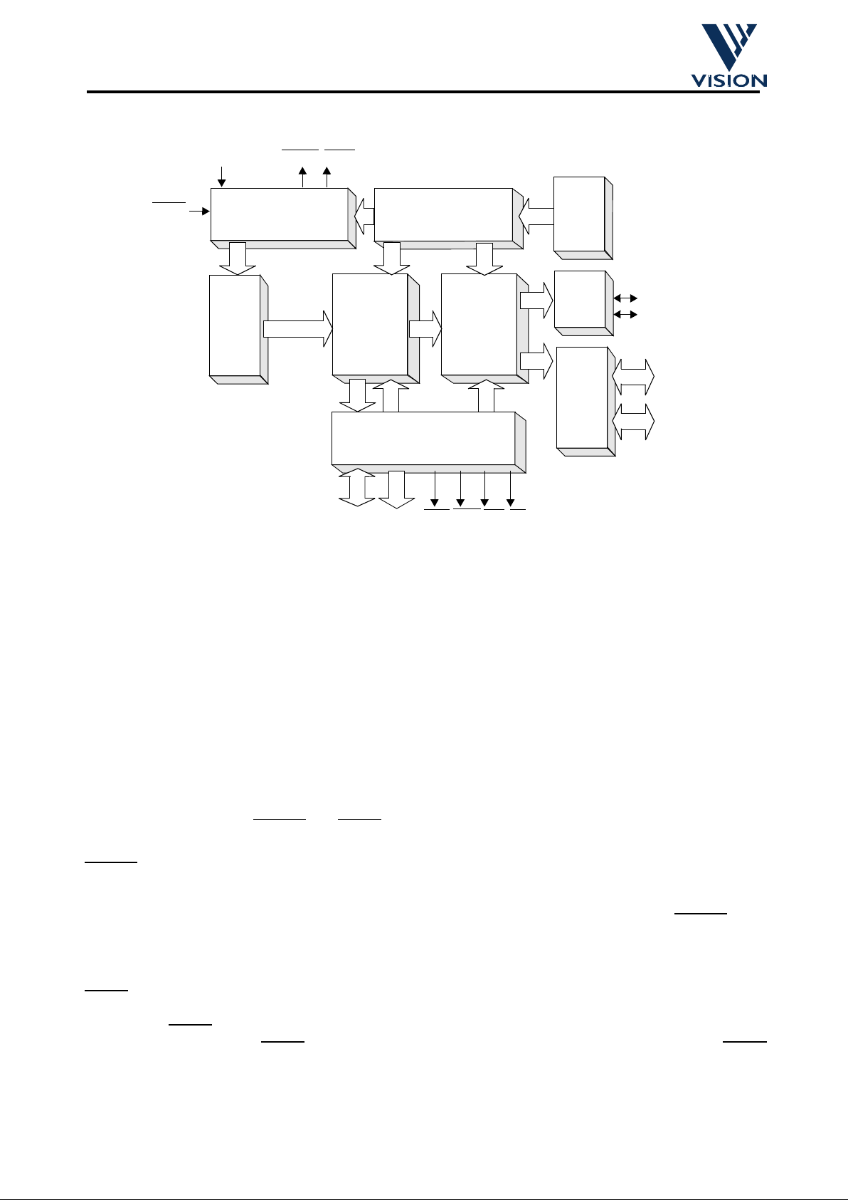
The power management block is primarily responsible for low-level control of system power, clocks and reset
se
q
uences to ensure ful l complian ce with the USB specifi cation and po wer saving modes of operation. This
module also includes a watc hdo
g
reset ensuring, for example, the system always returns to a safe state if
power-failure or an
y
other event has caused CPiA to encounter an unknown and fatal error.
CPiA re
q
uires up to 3 independent power supplies. When CPiA is designed into a product providing full USB
power consumptio n compliance, the s
y
stem must provide CPiA with VDD=5V, a switched VDDA=5V and
VDDU=3.3V
(
for internal USB differential pads). If CPiA is used in a target application where only the parallel
port interface is re
q
uired and slightly higher module power consump tion is permitted, a single, constant 5V
suppl
y
can be safely fed to VDD, VDDA and VDDU.
VDD and VDDU must alwa
y
s be permanently connected to system power supplies. The switched VDDA
power line is t
y
pically supplied using a power FET external to CPiA. The power management module
provides two outputs for drivin
g
the FET gates and hence is capable of enabling or disabling power to
s
y
stem-level components; LOPOW and NORM.
LOPOW
is asserted when CPiA is ready for VDDA to be powere d and once power has been applied puts
CPiA into a state where commands received from the host PC can be processed. As well as VDDA becomin
g
active, this also includes starting up of high-speed 14.318MHz a nd 48MHz clocks using external crystals,
resettin
g
and initialising all internal s tat e mac hines a nd logic within VP, VC and CP modules. LOPOW i s de-
asserted at an
y
time the host PC requests the module is either put into a US B SUSPEND cond ition or an
y
other host-application-dependent mode when ultra low power consumption is required.
NORM
is asserted when CPiA is ready to put the module i nto the highest power mode of operation which
occurs when the camera becom es activ e and hi
g
h speed image transfers via USB or pa rallel port i nterfa ces
commences. NORM
is used i n te rn a lly to CPiA only but is provided as an optional output for driving customer-
specific lo
g
ic. For example, N ORM can be used to il lumi nate an LED indic ating the camera is active. NORM
is also deasserted at any time the host requests USB SUSPEND mode.
VP VIDEO DATA
INTERFACE
POWER
MANAGEMENT
CP CONTROL
INTERFACE
USB
PARALLEL PORT
INTERFACE
D+
STREAMER
DATA
COMPRESSION
IMAGE
DRAM
CONTROLLER
D-
REGISTERS
Block Diagram of CPiA Video Compressor Module
CLK400H
RESET
LOW PO NORM
RAMA[8:0]
RAMD[15:0]
LCAS
UCAS
RAS
WE
Page 11
V:\apps\cpia\docs\cpia datasheet\cpia_datasheet4.fm
02/07/98 11
Colour Processor Interface ASIC
Commercial In Confidence
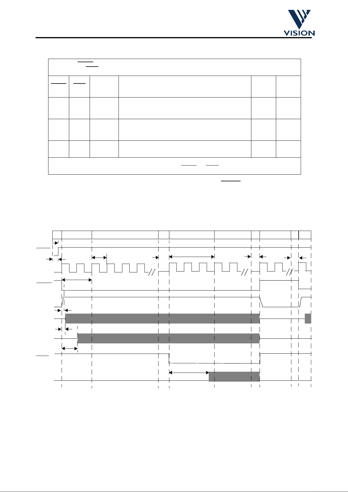
CPiA’s power management block requires two externally derived inputs: RESET provides a global reset to all
CPiA lo
g
ic and CLK400H provides a low frequency clock to CPiA’s internal power control state machines and
should be constrained in accordance with the timin
g
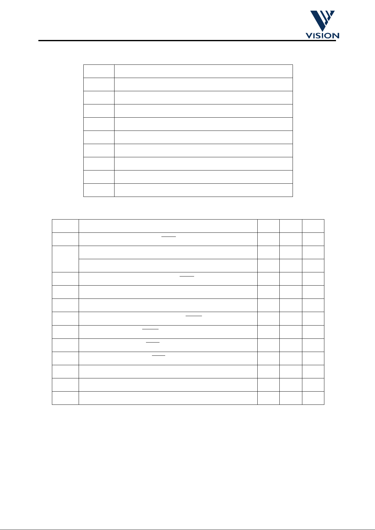
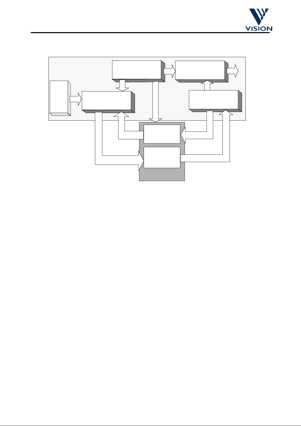
diagrams presented below. The Events are also
described in the table below. After event RR, the process returns to CSU.
Effect of LOPOW on CPiA-based module power consuption WITH EXTERNAL CONTROL OF VDDA using external FET.
NORM
is shown for reference only and is not required for power control using external FET.
LOPOW
NORM Mode Description VDDA
Approx
Module
Current
1 1 Suspend
CPiA, camera module and DRAM components are in lowest power
mode. VDDA is withdrawn as external FET is off, all fast clocks are
disabled and CPiA logic is in held reset
0V <500uA
0 1 Low Power
CPiA is in low power mode. Fast clocks enabled and CPiA can process
commands from host PC. Camera, video processing and DRAM
controller modules are held in reset
5V <50mA
0 0 High Power
All CPiA modules, camera and DRAM components are active and video
data is being transferred to host PC.
5V <250mA
If VDDA is not controlled using VDDA (VDD=VDDA=VDDU) in parallel port modes of operation, approx module power
consumption will be <250mA at all times. In such cases, LOPOW
and NORM can be considered redundant.
RESET
CLK400H
LOWPO
CKI14
CKI48
NORM
SCLK
VDDA
Event
POR
CSU LPM
RHP
HPI
HPM
SR
SUSP
RR CSU
Tp
Trp
Trl
Tck1su
Tck2su
Trvda
Tllp
Timing Diagram Highlighting Power Management Events
Tnsclk
Tnhpm
Trhp
Tsrs
Trrc
Page 12
V:\apps\cpia\docs\cpia datasheet\cpia_datasheet4.fm
02/07/98 12
Colour Processor Interface ASIC
Commercial In Confidence
Event Description
POR POWER ON RESET PROVIDED TO CPIA BY EXTERNAL HARDWARE
CSU HIGH FREQUENCY CLOCK START UP
LPM LOW POWER MODE OF CPIA OPERATION
RHP HOST REQUEST FOR CPIA TO ENTER HIGH POWER STATE
HPI INITIALISE HIGH POWER MODE OF OPERATION
HPM HIGH POWER MODE OF CPIA OPERATION
SR USB REQUEST POWER SAVING SUSPEND MODE OF OPERATION
SUSP CPIA HELD IN USB SUSPEND MODE
RR USB REQUEST RESUME TO RECOVER LOW POWER MODE OF OPERATION
Parameter Description min max Units
Trp CPiA global RESET
pulse width 0.1 - ms
Tp
CPiA CLK400H period 2.25 2.75 ms
CPiA CLK400 duty 20:80 80:20 -
Trl Time for low power mode after RESET
deasserted 0 Tp ms
Tck1su 14.318MHz Clock start-up time - Tp ms
Tck2su 48MHz Clock start-up time - (2*Tp)-1 ms
Trvda VDDA Power Supply rise time from LOWPO
asserted - Tp ms
Tllp Time from LOWPO
asserted to low power mode 2*Tp ms
Tnsclk Time from NORM
to camera interface active ms
Tnhpm Time from NORM
to high power mode ms
Trhp Time to acknowledge host request for high power mode ms
Tsrs Time for CPiA to acknowledge and act upon USB suspend mode request ms
Trrc Time for CPiA to acknowledge and act upon USB resume low power mode request ms
Page 13
V:\apps\cpia\docs\cpia datasheet\cpia_datasheet4.fm
02/07/98 13
Colour Processor Interface ASIC
Commercial In Confidence
2.2.2 Video Compression
In the discussion to follow the CP iA device is assumed to be interfaced to the the host PC via the USB ,
however the discussion e
q
ually well applies to the parallel port interface option that CPiA also provides.
The VP module provides the vid eo data stream to VC. The pixel-b ased compression al
g
orithm operates b
y
considering the differences bet ween consecutive frames and enco ding those differences i n a Run-Length
Buffer
(
RLB) held in external DRAM. The result is a run-length encoded stream of the changes from frame-to-
frame. The stream consists of run-len
g
ths of regions where no change has occurred, coded YCbYCr
(
YUV422) values of pixel-pairs which have changed significantly, additional codes to mark the start/end/length
of frame rows, a frame header detailin
g
parameters associated with the capture settings of the encoded data
and finall
y
codes to mark the end of the encoded frame.
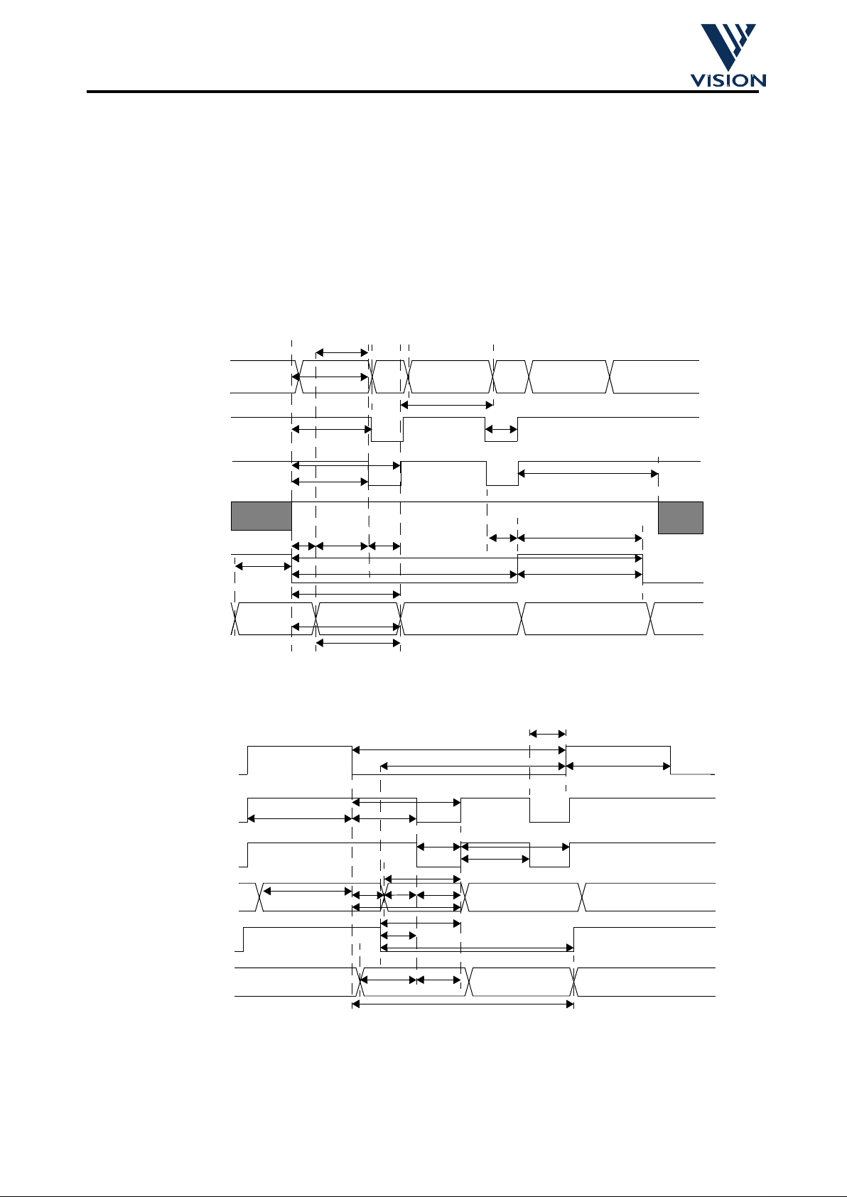
The VC module implements the compression al
g
orithm conceptually by way of two processes. The first
process is the Differencin
g
Engine/Run-Length Encoder (DE/RLE):
• Each pixel-pair of the curr ent video fr ame is comp ared in turn with the corres pondi n
g
pixel-pair s tored i n
the DRAM FrameStore
(FS)
. If this comparison indicates that there exists a significant dif f er ence in value
for the
g
iven pixel-pair then that pixel-pair’s value is stored at the next locationin the RLB .The stored value
is further coded to indicate its status as a pixel-pair value rather than a run-len
g
th . Conversely, if the
comparison indicates that the difference is not si
g
nificant, a run-length counter is incremented and stored
at the current po sition in the R LB. The lev el of
significant
difference is dynamically calculated by the CP
module from frame-to-frame and can be influenced b
y
the host PC. When th e DE/RLB f inishes proces sin
g
a frame the CP module is alerted indicating subsequent processes can commence.
The second process is the Data Streamer/Run-Len
g
th Decoder (DS/RLD):
• In parallel with the DE/RLE but dela
y
ed with respect to the current position in the RLB, the Data Streamer
(DS)
streams data from the RLB to USB interface module for transfer to the host. In addition, the DS also
decodes the RLB stream back into the FS thus updatin
g
it. The software driver also decodes the received
RLB stream on the host PC. When the DS/RLB reaches the end of the data stream the CP module is a
g
ain
alerted and the process repeats.
It is important to note that the two process es can run concurrentl
y
, that is the DE/RLE can be encoding the
current frame into th e RL B while at the same ti me the DE/ R LE c an b e s tr ea min
g
out the previously encoded
frame to the USB.
Framestore
EXTERNAL DRAM
encode
decode
CP MODULE
VIDEO COMPRESSION
Difference Engine &
Run Length Encoder
Run-Length
Buffer
HOST
PC
Video compression components and VC Module interfacing to External DRAM
USB/PP
INTERFACE
DATA STREAMER
Run Length Encoder
CPiA
modules
VP VIDEO DATA
INTERFACE
Page 14
V:\apps\cpia\docs\cpia datasheet\cpia_datasheet4.fm
02/07/98 14
Colour Processor Interface ASIC
Commercial In Confidence
2.2.3 DRAM Interface
In order to perform vi deo capture and compression, CPiA dep ends upon an a frame store provided by a
sin
g
le, low cost DRAM. The integral DRAM controller is designed to support standard 256K x 16 EDO
devices, with acces s t imes better than or e
q
ual to 60ns. Timing diagrams showing bus read and write cycles
are hi
g
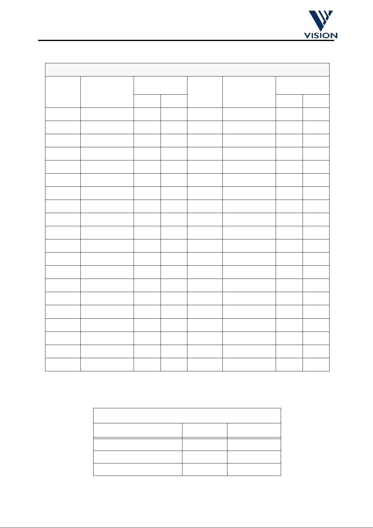
hlighted below. As seen in Se ction 2.2.2, the compression algorithm uses two main data struc tures
within the DRAM:
• The Fram estore holds a cop
y
of the previous image uploaded to the host. The DE us es this infor mation
to determine si
g
nificant differences between the FS image and the next image read from the VP.
• The Run Len
g
th Buffer stores the current frame in a run-length encoded form, ready for upload by the DS/
USB to the host.
RAMD[15:0]
RAMLCAS_n
RAMUCAS_n
RAMWE_n
RAMRAS_n
RAMA[8:0]
t
ASR
t
RC
t
RAS, tRASP
t
RP
t
CRP
t
AR
t
ACH
row col col row col
t
CAH
t
ASC
t
RAH
t
RSH
t
RRH, tRCH
t
CAS, tCLCH
t
AA
t
RAC
DATA
VALID
XX XX
XX
XX
t
CPA
t
OFF
t
CAC
t
CLZ
t
RCD
t
CSH
t
RCS
t
CHR
DRAM Read Cycle Timin
g
RAMD[15:0]
RAMLCAS_n
RAMUCAS_n
RAMWE_n
RAMRAS_n
RAMA[8:0]
DRAM Write C
y
cle Timin
g
t
RASP
t
RSH
t
RP
t
RWL
t
CSH
t
CRP
t
RCD
t
CAS
t
CLCH
t
PC
t
CP
row
col
row
col
DATA VALID
t
CAH
t
ASC
t
ACH
t
AR
t
RAH
t
ASR
t
CWL
t
WCS
t
WP
t
WCR
t
DS
t
DH
Page 15
V:\apps\cpia\docs\cpia datasheet\cpia_datasheet4.fm
02/07/98 15
Colour Processor Interface ASIC
Commercial In Confidence
Note 1 - DRAM timing para meters extracted from DRAM manufacturer ‘s -6 worst- case spe c dat a tables. Due to some variatio n in m anufact ure r’s figures it
is recommended required values presented in this table are closely checked against the data tables from specific target DRAM manufacturers.
Note 2 - Min and Max timing derived fro m wor st and best ca se design simu latio n wih respect to proc ess param eter derat ing wi th supply volt age a nd T j . All
timing parameters listed have been verified and validated through device characterisation with Ta@25C, VDD=VDDA=5V.
CPIA DRAM Interface Timing Parameters
Parameter
DRAM
requirement (ns)
Note 1
CPiA DRAM Timing (ns)
Note 2
Parameter
DRAM
requirement (ns)
Note 1
CPiA DRAM Timing (ns)
Note 2
min max min max
t
AA
>30 43 58 t
CAS
>10 28 40
t
ACH
>15 52 58 t
CAH
>10 28 40
t
AR
>45 68 72 t
CHR
>10 28 40
t
ASC
>0 17 21 t
CLCH
>10 28 40
t
ASR
>0 68 72 t
CLZ
0 0 0
t
CAC
>17 19 26 t
CP
>8 28 40
t
CRP
>5 68 72 t
CPA
>35 62 65
t
CSR
>5 28 40 t
CSH
>45 68 72
t
DH
>10 28 40 t
CWL
>10 52 57
t
DS
>0 28 40 t
OFF
0<t
OFF<
15 5.5 6
t
RAC
>60 63 67 t
PC
>25 68 72
t
RAS
>60 68 72 t
RAH
>10 11 21
t
RRH
>0 68 72 t
RASP
>60 68 72
t
RCD
14<t
RCD<
45 28 40 t
RC
>105 136 144
t
RCS
>0 28 40 t
RCH
>0 68 72
t
RP
>40 68 72 t
REF
<8ms - 16us
t
RWL
>15 52 57 t
RPC
>5 28 40
t
WCH
>10 28 40 t
T
<2 0.5 2
t
WCS
>0 17 20 t
WCR
>45 68 72
t
WP
>5 52 57 t
RSH
>15 28 40
Framestore and Run Length Buffer DRAM partitioning
Data Structure Size
(by
tes
)
Size (Kbytes
)
Framestore (FS
)
202752 198
Run-Len
g
th Buffer (RLB
)
205124 ~201
Total (FS + RLB
)
407876 ~399
Page 16

V:\apps\cpia\docs\cpia datasheet\cpia_datasheet4.fm
02/07/98 16
Colour Processor Interface ASIC
Commercial In Confidence
2.2.4 USB Interface
The USB interface is fully compliant with USB Specific at ion Version 1.0. The USB interface is des igned such
that the camera attaches to the PC via a 4-wire USB cable, either directl
y
at the PC motherboard USB
connector
(
root hub) or via a USB hub (in turn connected to the PC motherboard root hub). The USB hub
ma
y
be either a stand-alone USB hub device or a compound USB hub device incorporated, for example, in a
USB monitor or printer.
USB transfers bot h si
g
nal and power over the 4-wire cable such that the camera i s powered f rom the sam e
cable/connector over wh ich it communicates with the P C. The 4-wire cable carries VB us
(
nominally +5V at
the source
)
and GND wires to de liver power to devic es and differential data lines, D+ and D-. The c lock is
transmitted encoded alon
g
with the differential da ta. The clock en coding scheme is NRZI with bit stu ffing to
ensure ade
q
uate transitions. A SYNC field precedes each packet to allow the receiver(s) to synchronise their
bit recover
y
clocks. CPiA provides fully compliant USB differential pads on-chip so there is no need to use an
external, discrete bus tranceiver chip such as Philips’ PDIUSBP11. In accordance with the USB Specification
Version 1.0, the pads have been characterised for correct operation up to the maximum peripheral cabl e
len
g
th of 5m.
2.2.4.1 CPiA-Based USB Camera
The CPiA-based USB ca mera is a high-power, bus-powered device. When it is firs t attached to a USB hub
port it operates in its low-power mode consumin
g
no more than 100mA. Once the camera has been
successfull
y
enumerated it may operate in its high-power mode in whic h it consu mes no mo re than 400mA .
Since the camera is a h i
g
h-power, bus-powered device it will only enumerate successfully if connected to a
self-powered USB hub.
(
A bus-powered USB hub is only capable of supplying 100mA at each of its
downstream ports
)
.
The CPiA-based USB camer a responds to suspend si
g
nalling issued by the USB (more than 3ms of bus
IDLE time
)
. In its suspend mode of oper ation the came ra draws no mo re than 500u A. The camera do es not
support remote wakeup.
The CPiA USB camera is a sin
g
le Configuration, single Interface USB pe ripheral d evice. I ts single Interface
(
Interface 1) supports Control Endpoint 0 and Isochronous IN Endpoint 1.
All devices must support Control Endpoint 0 as this is the endpoint with which the PC communicates over the
default pipe at device enumeration time. CPiA utilises Control Endpoint 0 to respond to standard USB
commands
(
such as those used at de vice enum eration time) and to Vendor specific CPi A comman ds which
are used to control the operation of the camera and to re
q
uest status information from the camera. Note that
the camera does n ot suppo rt a US B Class S pecificati on and so onl
y
Vendor commands are used to cont rol
the operation of the camera.
Isochronous IN Endpoin t 1 is used to transfer video d ata from the c amera to the PC. U sin
g
an isochronous
endpoint for this task
g
uarantees bandwidth and latency for the transfer of video data. The bandwidth
re
q
uested for video data transfer can be varied by means of the four defined Alternate Settings of Interface 1.
2.2.4.2 USB Control Transfers
Control transfers are used to pas s control in formation to th e CPiA-based USB camer a from the hos t and to
re
q
uest state information back from the camera. For example, control transfers are used at device
enumeration time when the host PC re
q
uests information about the USB device which has been dynamicall
y
attached to the bus t o enable it to lo ad the appropriate driver(s). (USB Device Enumerati on is discussed i n
detail in section
2.2.4.3
)
. CPiA uses Control Endpoint 0 for all control transfers. Therefore Endpoint 0 handles
both standard USB commands and Vendor specific CPiA commands.
A control transfer consists of three phases: a SETUP phase, a DATA phase
(
should one exist) and a STATUS
phase.
Page 17

V:\apps\cpia\docs\cpia datasheet\cpia_datasheet4.fm
02/07/98 17
Colour Processor Interface ASIC
Commercial In Confidence
The SETUP phase contains details of the command being sent to the camera including, the specific command
re
q
uest, whether the co mmand is a WRITE (host to camera) or READ (camera to host) command and the
number of b
y
tes expected in the DATA phas e. (For further informati on on the S ETUP phas e please r efer to
USB Specification Version 1.0, Section 9.3
)
.
The DATA phase i s used to tra nsfer a number o f b
y
tes of informati on associated with the comm and to the
camera if this is a W RITE command or from the ca mera if this is a READ co mmand. The DATA phase can
consist of a number of discrete DATA transactions on the bus. With CPiA-based USB cameras, data is
transfered in 8-b
y
te packets with the remaining data bytes transfered in the last data transa ction being less
than 8 b
y
tes if the total number of bytes to be transfered is not a m ult ipl e of 8 . This is bec au se the m ax imu m
packet size of Control Endpoint 0 in CPiA is 8 b
y
tes.
The STATUS phase is used to indicate w hether or not all was well with the SETUP and DATA phas es and
conse
q
uently whether or not the control transfer has completed successfully. If at any time the camera
receives an unreco
g
nised command (for example due to data c orrupti on on the US B) or it cannot process a
valid command for some reason it returns a STALL handshake on the bus to indicate to the host that
somethin
g
is wrong.
2.2.4.3 USB Device Enumeration
The USB hub detects that a high speed USB device has been dynamically attached to one of its downstream
ports b
y
the presence of a 1.5KOhm pul l-up resist or on the D+ differential data line on the u pstream port of
the device, as i s the case with a CPiA-based USB camera. Before the port to which t he camera has bee n
connected can be enabled the hub ensures that the device is reset. It does this b
y
issuing SE0 reset
si
g
nalling on the USB differential data lines for at least 10ms and then enables the port. This causes the
camera to ‘listen’ to USB traffic at bus address 0 until such tim e as it is assi
g
ned its own unique USB bus
address. The camera is read
y
to respond to host access within 10ms of this reset signalling being de-
asserted. Note that the hub waits a specified dela
y
time after device attach before issuing the reset signallin
g
to ensure the device’s internal power supply has stabilised.
Now that the camera is listenin
g
at bus address 0 the host begins to communicate with the camera. The initial
communications comprise the device enumeration traffic se
q
uence. The host first issues a
GetDescriptor
(
DEVICE) command (SETUP Packet
80 06 00 01 00 00 40 00)
to Control Endpoint 0 (which all USB devices
must support
)
at bus address 0. The host only receives the first 8 data bytes of the DATA phase of this control
transfer
(
that is, the first DATA transaction within the DATA phase) before issuing the STATUS phase.
The host then issues a
SetAddress
command (SETUP Packet
00 05 yz wx 00 00 00 0 0
where wxyz is the
USB device address
)
to assign a unique USB bus addre ss to the ca mer a. Foll owi ng the STATUS phase of a
successful
SetAddress
command the camera then ‘listens’ and responds to USB traffic at this unique
address onl
y
.
The host continues b
y
issuing a
GetDescriptor
(DEVICE) command (SETUP Packet
80 06 00 01 00 00 12 00
)
.
In response to the
GetDescriptor
(DEVICE) command the camera
returns its DEVICE descriptor which
comprises 18 bytes of information. The DEVICE descriptor describes general information about the USB
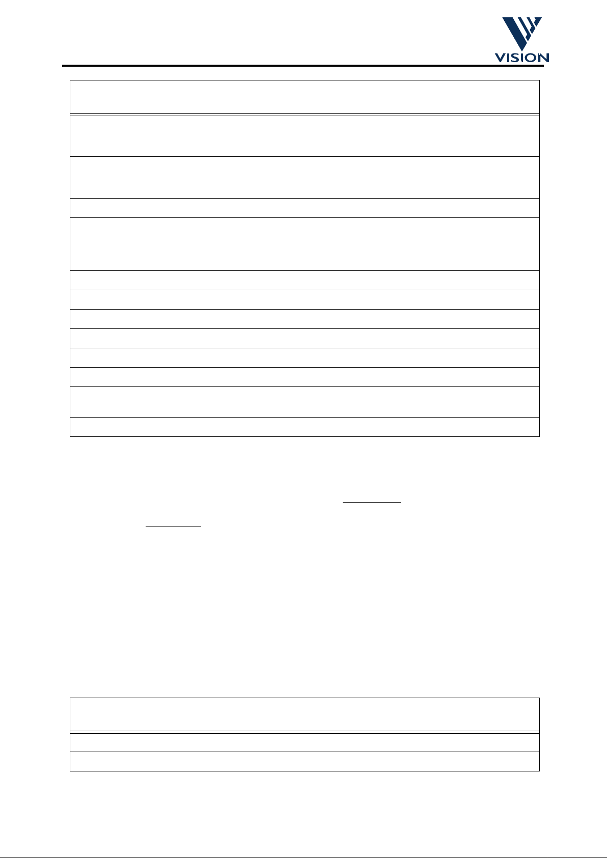
device. The table below shows the DEVICE descriptor information returned by a CPiA-based USB camera in
response to the
GetDescriptor
(DEVICE) command. This information c an be ch ec ke d at device enume ra tio n
time using a USB bus analy ser such as the CATC Inspector when debugging a CPiA-based USB camera
design.
Descriptor Field
Size
(bytes)
Value Description
bLength
1 0x12 Size of this descriptor in bytes.
bDescriptorType
1 0x01 DEVICE Descriptor Type.
Page 18
V:\apps\cpia\docs\cpia datasheet\cpia_datasheet4.fm
02/07/98 18
Colour Processor Interface ASIC
Commercial In Confidence
Notes:
(1)
The CPiA device returns a Product ID as part of its DEVICE descriptor. This Product ID is used along with
the Vendor ID to load the approriate device driv ers for the CPiA -based USB came ra. The device can return
two possible Product ID numbers dependin
g
on the state of t he ID_ SEL ECT pin. This pin has an internal pull-
up resistor which, when not connected, provides a Product ID of 0x0002 for a USB-onl
y
CPiA-based camera
module. When the ID_SELECT
pin is pulled low externally, the Product ID will be 0x0001, which is used for a
combined parallel port and USB module.
(2)
The USB camera does no t support String Descriptors.
Any request by the host for a STRING descr iptor
will cause the camera to STALL the default pipe.
Finall
y
the host issues a
GetDescriptor
(CONFIGURATION) command (SETUP Packet
80 06 xx 02 00 00 FF
00
)
.
CPiA has only one Configuration (index xx = 00). If xx is anything other than 00 CP iA will STALL the
default pipe.
In response to the
GetDescriptor
(CONFIGURATION) command the camera
returns its
Configuration, Interface and Endpoint descriptors which comprise 73 bytes of information.
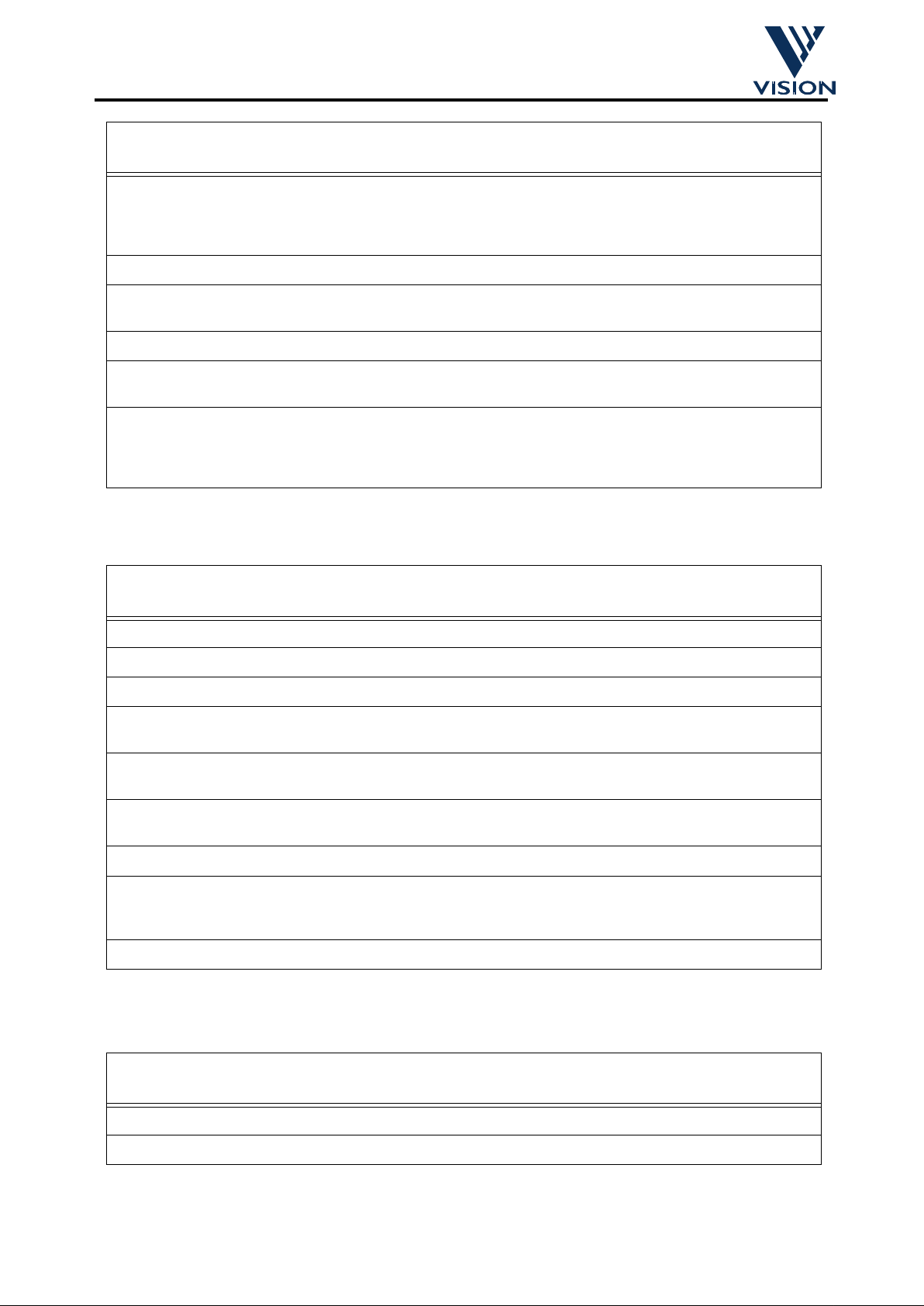
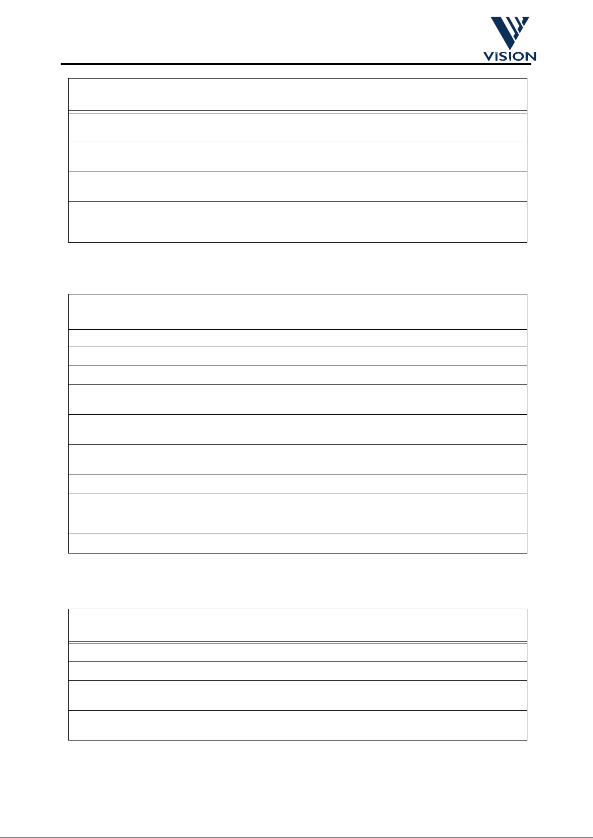
The tables below sho w th e d es cri ptor info rmati on r eturne d by a CPiA-based USB c ame ra in r es po nse to the
GetDescriptor
(CONFIGURATION) c ommand. This info rmation ca n be checked a t device enumer ation time
using a USB bus analyser such as the CATC Inspector when debugging a CPiA-based USB camera design.
bcdUSB
2 0x0100 USB Specification Release Number identifying the
release of the USB Sp ecific ation that t he device and its
descriptors are compliant with. (Release 1.00)
bDeviceClass
1 0x00 Class Code (assigned b y USB). This field i s set to 0x 00
meaning that the class information is specified in the
Interface descriptor.
bDeviceSubClass
1 0x00 Subclass Code (assigned by USB).
bDeviceProtocol
1 0x00 Protocol Code (assigned by USB). This field is set to
0x00, meaning that the device does not use class specific protocols on a device basis, however may use
class specific protocols on an interface basis.
bMaxPacketSize0
1 0x08 Maximum packet size for Endpoint 0.
idVendor
2 0x0553 Vendor ID (assigned by USB).
idProduct
2 0x0002
(1)
Product ID (assigned by the manufacturer).
bcdDevice
2 0x0100 Device release number in binary-coded decimal.
iManufacturer
10x00
(2)
Index of string descriptor describing manufacturer.
iProduct
10x00
(2)
Index of string descriptor describing product.
iSerialNumber
10x00
(2)
Index of string descriptor describing the device’s serial
number.
bNumConfigurations
1 0x01 Number of possible configurations
Descriptor Field
Size
(bytes)
Value Description
bLength
1 0x09 Size of this descriptor in bytes.
bDescriptorType
1 0x02 CONFIGURATION Descriptor Type.
Descriptor Field
Size
(bytes)
Value Description
Page 19
V:\apps\cpia\docs\cpia datasheet\cpia_datasheet4.fm
02/07/98 19
Colour Processor Interface ASIC
Commercial In Confidence
wTotalLength
2 0x0049 Total length of data returned for this configuration.
Includes the combined length of all descriptors (configuration, interface, endpoint, and class or vendor specific) returned for this configuration.
bNumInterfaces
1 0x01 Number of interfaces supported by this configuration.
bConfigurationValue
1 0x01 Value to use as an argument to
SetConfiguration
to
select this configuration.
iConfiguration
10x00
(1)
Index of string descriptor describing this configuration.
bmAttributes
1 0x80 Configuration characteristics: Bus Powered and no
Remote Wakeup.
MaxPower
1 0xC8 Maximum power consumption of USB device from the
bus in this specific configuration when the device is
fully operational. Expressed in 2mA units ( 0xC8 =
400mA).
Descriptor Field
Size
(bytes)
Value Description
bLength
1 0x09 Size of this descriptor in bytes.
bDescriptorType
1 0x04 INTERFACE Descriptor Type.
bInterfaceNumber
1 0x01 Number of interface.
bAlternateSetting
1 0x00 Value used to select alternate setting for the interface
identified in the prior field.
bNumEndpoints
1 0x01 Number of endpoints used by this interface (excluding
Endpoint 0).
bInterfa ceClass
1 0xFF Class code (assigned by USB). A v alue of 0xFF means
that the interface class is vendor specific.
bInterfaceSubClass
1 0x00 Subclass code (assigned by USB).
bInterfaceProtocol
1 0xFF Protocol code (assigned by USB). A value of 0xFF
means that the device uses a vendor specific protocol
for this interface.
iInterface
10x00
(1)
Index of string descriptor describing this interface.
Descriptor Field
Size
(bytes)
Value Description
bLength
1 0x07 Size of this descriptor in bytes.
bDescriptorType
1 0x05 ENDPOINT Descriptor Type.
Descriptor Field
Size
(bytes)
Value Description
Page 20
V:\apps\cpia\docs\cpia datasheet\cpia_datasheet4.fm
02/07/98 20
Colour Processor Interface ASIC
Commercial In Confidence
bEndpointAddress
1 0x81 The address of the endpoint on the USB device
described by this descriptor: (IN endpoint, number 1)
bmAttributes
1 0x01 Field describing the endpoint’s attributes: Isochronous
transfer type.
wMaxPacketSize
2 0x0000/
0x0000
(2)
Maximum packet size this endpoint is capable of sending: 0 bytes or 0 bytes
(2)
.
bInterval
1 0x01 Interval for polling endpoint for data transfers (in ms).
For isochronous endpoints this field must be set to 1
(ie. every USB frame).
Descriptor Field
Size
(bytes)
Value Description
bLength
1 0x09 Size of this descriptor in bytes.
bDescriptorType
1 0x04 INTERFACE Descriptor Type.
bInterfaceNumber
1 0x01 Number of interface.
bAlternateSetting
1 0x01 Value used to select alternate setting for the interface
identified in the prior field.
bNumEndpoints
1 0x01 Number of endpoints used by this interface (excluding
Endpoint 0).
bInterfa ceClass
1 0xFF Class code (assigned by USB). A v alue of 0xFF means
that the interface class is vendor specific.
bInterfaceSubClass
1 0x00 Subclass code (assigned by USB).
bInterfaceProtocol
1 0xFF Protocol code (assigned by USB). A value of 0xFF
means that the device uses a vendor specific protocol
for this interface.
iInterface
10x00
(1)
Index of string descriptor describing this interface.
Descriptor Field
Size
(bytes)
Value Description
bLength
1 0x07 Size of this descriptor in bytes.
bDescriptorType
1 0x05 ENDPOINT Descriptor Type.
bEndpointAddress
1 0x81 The address of the endpoint on the USB device
described by this descriptor: (IN endpoint, number 1)
bmAttributes
1 0x01 Field describing the endpoint’s attributes: Isochronous
transfer type.
Descriptor Field
Size
(bytes)
Value Description
Page 21
V:\apps\cpia\docs\cpia datasheet\cpia_datasheet4.fm
02/07/98 21
Colour Processor Interface ASIC
Commercial In Confidence
wMaxPacketSize
20x01C0/
0x0140
(2)
Maximum packet size this endpoint is capable of sending: 448 bytes or 320 bytes
(2)
.
bInterval
1 0x01 Interval for polling endpoint for data transfers (in ms).
For isochronous endpoints this field must be set to 1
(ie. every USB frame).
Descriptor Field
Size
(bytes)
Value Description
bLength
1 0x09 Size of this descriptor in bytes.
bDescriptorType
1 0x04 INTERFACE Descriptor Type.
bInterfaceNumber
1 0x01 Number of interface.
bAlternateSetting
1 0x02 Value used to select alternate setting for the interface
identified in the prior field.
bNumEndpoints
1 0x01 Number of endpoints used by this interface (excluding
Endpoint 0).
bInterfa ceClass
1 0xFF Class code (assigned by USB). A v alue of 0xFF means
that the interface class is vendor specific.
bInterfaceSubClass
1 0x00 Subclass code (assigned by USB).
bInterfaceProtocol
1 0xFF Protocol code (assigned by USB). A value of 0xFF
means that the device uses a vendor specific protocol
for this interface.
iInterface
10x00
(1)
Index of string descriptor describing this interface.
Descriptor Field
Size
(bytes)
Value Description
bLength
1 0x07 Size of this descriptor in bytes.
bDescriptorType
1 0x05 ENDPOINT Descriptor Type.
bEndpointAddress
1 0x81 The address of the endpoint on the USB device
described by this descriptor: (IN endpoint, number 1)
bmAttributes
1 0x01 Field describing the endpoint’s attributes: Isochronous
transfer type.
wMaxPacketSize
20x02C0/
0x0268
(2)
Maximum packet size this endpoint is capable of sending: 704 bytes or 616 bytes
(2)
.
bInterval
1 0x01 Interval for polling endpoint for data transfers (in ms).
For isochronous endpoints this field must be set to 1
(ie. every USB frame).
Descriptor Field
Size
(bytes)
Value Description
Page 22
V:\apps\cpia\docs\cpia datasheet\cpia_datasheet4.fm
02/07/98 22
Colour Processor Interface ASIC
Commercial In Confidence
Notes:
(1)
The USB camera does no t support String Descriptors.
Any request by the host for a STRING descr iptor
will cause the camera to STALL the default pipe.
(2)
The first number shows maximum packet size values returned when USB_BANDWIDTH is left
unconnected
(
internally pulled up), as is the case in norma l operation. If USB_BANDWIDTH is pulled LO
externall
y
the second number i s returned as the maximum packet size for the isochronous e ndpoint. For
further information see section
2.2.4.4
.
On successful completi on of thes e control tr ansfers the host has
g
athered all relevant in formatio n about the
Descriptor Field
Size
(bytes)
Value Description
bLength
1 0x09 Size of this descriptor in bytes.
bDescriptorType
1 0x04 INTERFACE Descriptor Type.
bInterfaceNumber
1 0x01 Number of interface.
bAlternateSetting
1 0x03 Value used to select alternate setting for the interface
identified in the prior field.
bNumEndpoints
1 0x01 Number of endpoints used by this interface (excluding
Endpoint 0).
bInterfa ceClass
1 0xFF Class code (assigned by USB). A v alue of 0xFF means
that the interface class is vendor specific.
bInterfaceSubClass
1 0x00 Subclass code (assigned by USB).
bInterfaceProtocol
1 0xFF Protocol code (assigned by USB). A value of 0xFF
means that the device uses a vendor specific protocol
for this interface.
iInterface
10x00
(1)
Index of string descriptor describing this interface.
Descriptor Field
Size
(bytes)
Value Description
bLength
1 0x07 Size of this descriptor in bytes.
bDescriptorType
1 0x05 ENDPOINT Descriptor Type.
bEndpointAddress
1 0x81 The address of the endpoint on the USB device
described by this descriptor: (IN endpoint, number 1)
bmAttributes
1 0x01 Field describing the endpoint’s attributes: Isochronous
transfer type.
wMaxPacketSize
20x03C0/
0x0380
(2)
Maximum packet size this endpoint is capable of sending: 960 bytes or 896 bytes
(2)
.
bInterval
1 0x01 Interval for polling endpoint for data transfers (in ms).
For isochronous endpoints this field must be set to 1
(ie. every USB frame).
Page 23
V:\apps\cpia\docs\cpia datasheet\cpia_datasheet4.fm
02/07/98 23
Colour Processor Interface ASIC
Commercial In Confidence
camera and is able to load the ap propriate drivers for the camer a. Once this has been done the camer a is
said to be enumerated.
2.2.4.4 USB Isochronous Transfers
As stated in sect ion
2.2.4.1
, Isochronous IN Endpoint 1 is used to transfer video data from the camera to the
host. Interface 1 has four Al ternate Settin
g
s defined allowing different USB bandwidth s to be requested for
this transfer of video dat a. Fu rther more , i t i s pos si ble t o u se the US B_ BANDW IDTH
input to select a se cond
set of Alternate Settin
g
isochronous bandwidt hs. In nor m al op er ati on US B_ BA NDW IDTH is left unconnected
(
internally pulled up). If it is pulled LO externally a second set of A lternate Setting isochronous ban dwidths
are used. The table below shows the Alternate Settin
g
isochronous bandwidths of Endpoint 1 for both
USB_BANDWIDTH
HI and LO.
Note that the second set of Al ternate Set tin
g
bandwidths available by pulling USB_BANDWIDTH LO allow a
sli
g
htly lower set of bandwidth settings to be used.
The isochronous bandwidt h is reported as the number of b
y
tes per USB frame. The USB is framed into 1ms
time slots.
Alternate Settin
g
0 is always 0 bytes/ms. This ensures that we can select an Alternate Setting for the camera
where no bandwidth is reserv ed. A lternate Settin
g
0 is the default Alternate Setting selected when the CPiA
USB driver is loaded, su ch that wh en the ca mera i s enumera ted but not in operati on
(
no application is usin
g
the camera hardware to transfer video data) then no USB bandwidth is requested. This is esse ntial f or a USBfriendl
y
peripheral such that other devices may use the full potential of the bus at this time.
When an application w ishes to use the camer a the CPiA USB driv er will re
q
uest isochronous bandwid th for
the trans fer of vide o dat a. I t wil l st art b
y
requesting the largest bandwidth supported by CPiA, that is Alternate
Settin
g
3, to ensure the best possibl e framerate by default. If the USB bus has many isochronous devices
attached and Alternate Settin
g
3 cannot be supported the CPiA USB driver will then request Alternate Settin
g
2 and if necessary Alternate Setting 1 to guarantee bandwidth for the transfer of video data. If even the
bandwidth re
q
uirement of Alternate Setting 1 cannot be supported by the bus at that time the user will have to
stop usin
g
another isochronous device to free-up isochronous bus time to allow the USB camera to operate.
Additionall
y
, the camera user ca n select the USB bandwi dth they wish to use by means of the Mul timedia
Control Panel S ettin
g
s Dialogue for the camera. Here they can select High (Alternate Setting 3), Medium
(
Alternate Setting 2) or Low (Alternate Setting 1) USB bandwidth. Thus if the CPiA camera is current ly usin
g
High bandwidth and they wish to connect and simultaneously use another isochron ous US B de vi ce they can
manuall
y
force the CPiA camera to use less bandwidth by selecting Medium or Low bandwidth settings.
Obviousl
y
this may result in lower framerate video (depending on the current compression setting).
Once an Alternate Settin
g
has been selected and is supported by the bus then the CPiA camera has
g
uaranteed bandwidth and latency for the transfer of video data. This means that in every 1ms USB time slot
an IN token will be issued to the CPiA Endpoint 1 for the transfer of up to
MaxPacketSize
bytes of video data,
where
MaxPacketSize
is the reserved b andwidth per ms . The CPiA camera will transfer as muc h data as it
currentl
y
has available up to
MaxPacketSize
. When no compression is selected then
MaxPacketSize
bytes of
video data will be transfered in ever
y
USB frame. If compression is selected then less than
MaxPacketSize
bytes of video data may be transfered depending on the level of compression requested. When the device is
Alternate Setting
Isochronous bandwidth per ms
USB_BANDWIDTH=1 (default)
Isochronous bandwidth per ms
USB_BANDWIDTH=0
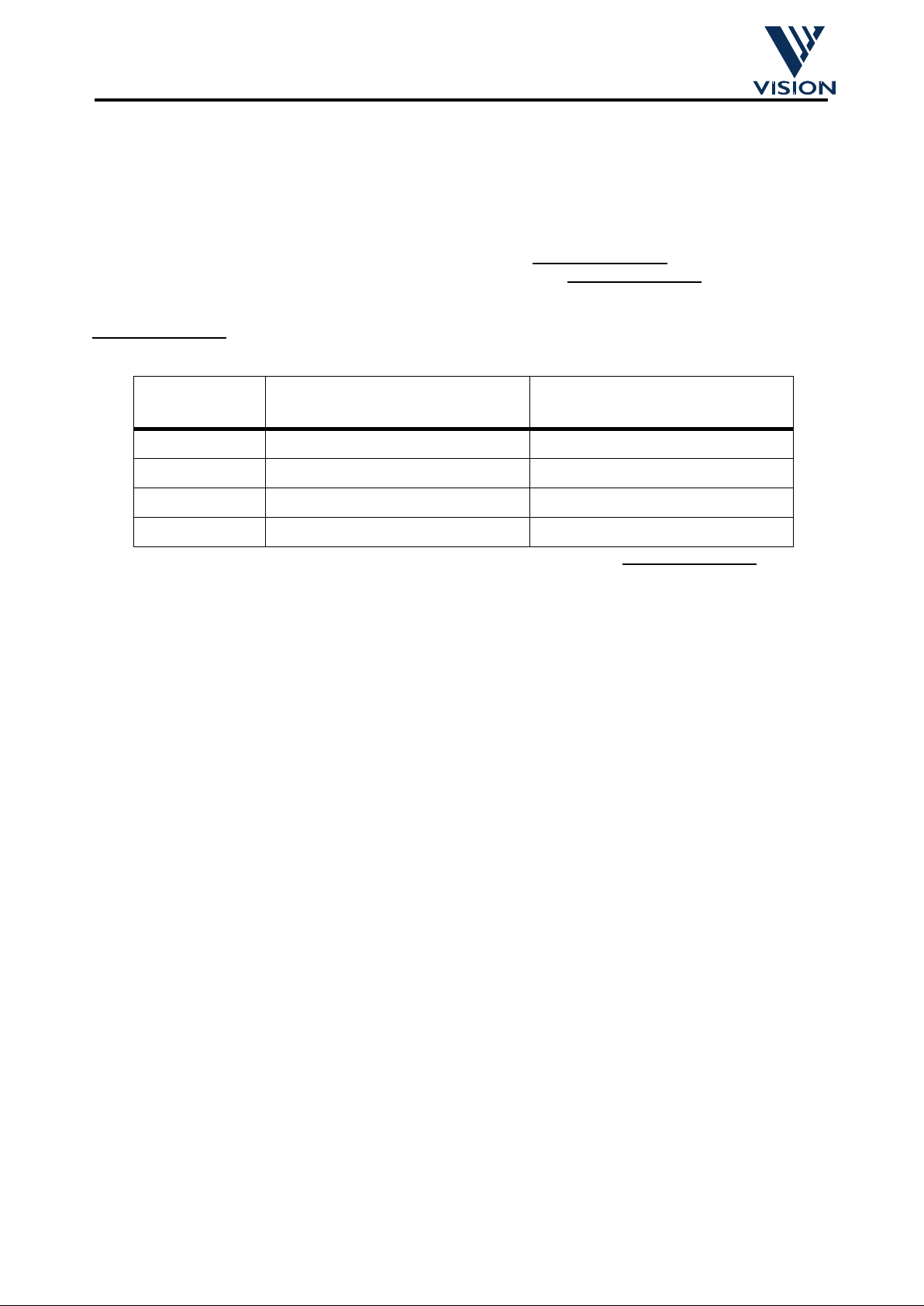
00 b
y
tes 0 bytes
1 448 bytes 320 bytes
2 704 b
y
tes 616 bytes
3 960 bytes 896 bytes
Page 24

V:\apps\cpia\docs\cpia datasheet\cpia_datasheet4.fm
02/07/98 24
Colour Processor Interface ASIC
Commercial In Confidence
sending a compressed i mage stream to the hos t the amount of data to be sent for ea ch image frame can
var
y
, depending on the compress io n ratio achieved. To enable the host to detect the end o f v al id im age data
the device inserts four
0xFF
values into the image stream to mark the end of image frame. As a sequence of
four 0xFF values will never occur within a valid frame of ima
g
e data the host can use this to simply detect the
end of the ima
g
e data, without having to decompress the im age. The host driver che cks the inte rgrity of the
ima
g
e data stream before it is decoded. If any corruption is d etected the frame is discarde d and another
uploaded.
Page 25
V:\apps\cpia\docs\cpia datasheet\cpia_datasheet4.fm
02/07/98 25
Colour Processor Interface ASIC
Commercial In Confidence
2.2.5 Parallel Port Interface
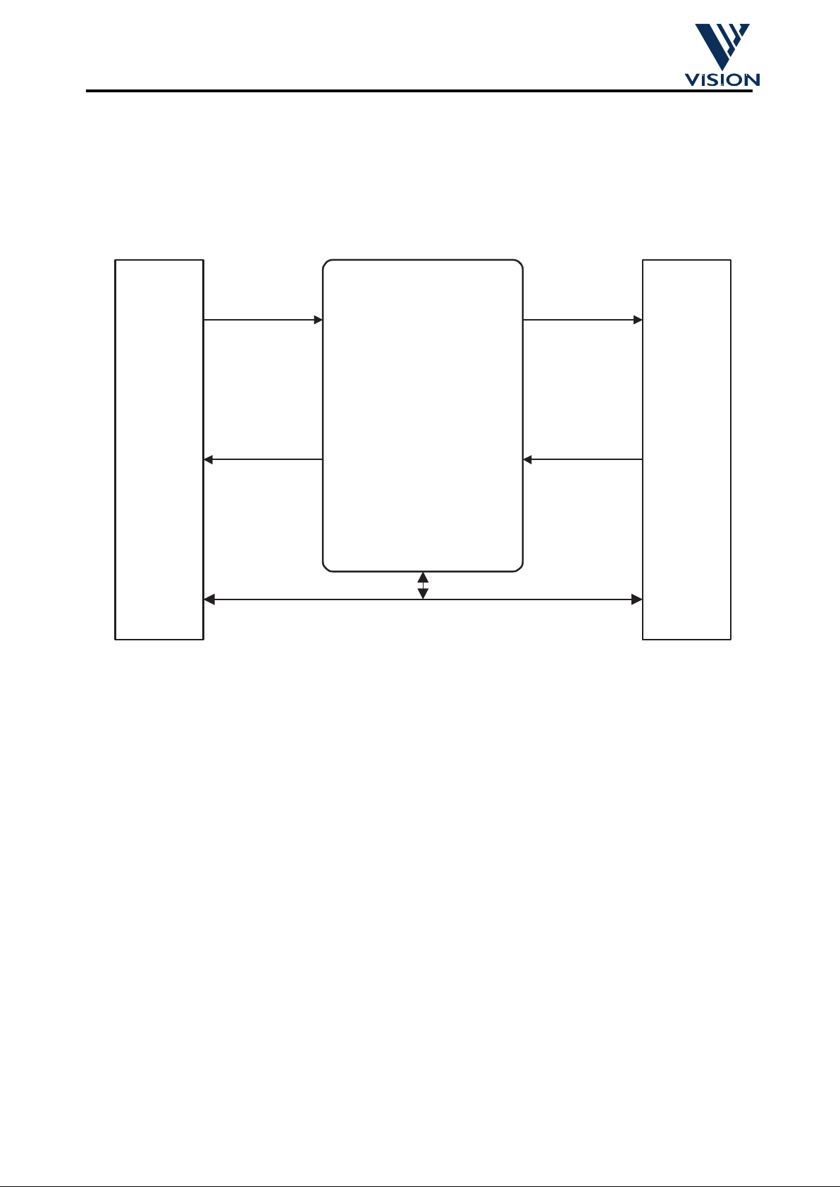
The parallel port interface is designed to attach directly to the parallel printer port of a PC. As such it contains
8 bi-directional data lines , 4 control inputs and 5 status outputs for conne ction to the host parallel port. In
addition, a further 4 outputs, 5 inputs ar e provided to suppor t pass-throu
g
h parallel port de signs. These two
ports are referred to as the
Host Port
and
Pass-through Port.
Figure 2.5 : Parallel Port Interface Signals
This followin
g
sections give a guide to the low level protocols used to transfer command and image data over
the parallel port interface. The
y
should be read in co njunction with the docu men t "IEEE St d 128 4 - Standar d
Si
g
naling method for a Bidirectional Par allel Peripheral Interface for Pers onal Computers". It is intended to
g
ive users enough information to design and debug boards utilising the CPiA device.
2.2.5.6 Para llel Port Protocol
There are three classes of transfer that take place over the parallel port.
• IEEE Std 1284 Device ID Transfers
• Command / Status Transfers
•Ima
g
e Stream Transfers
1284 Device ID transfers are used b
y
the Microsoft Windows 95/98 operating systems to detect the presence
of the CPiA-based camera at boot time and load the approriate drivers.
Command and Status transfers are used to pass control information to the CPiA-based camera from the host
as well as returnin
g
state information back to the host.
Ima
g
e Stream Transfers are used to transfer image data from CPiA to the host. This data can be in a
compressed or uncompressed format dependin
g
on how the CPiA has been set up via the associated host PC
software driver.
Host PC
Parallel
Port
Pass-
through
Port
Control Control
Status Status
Data
CPiA Device
Data
H_STROBE
H_AUTOFD
H_INIT
H_SELECTIN
H_FAULT
H_ACK
H_BUSY
H_PERROR
H_SELECT
HP_DATA0:7
P_STROBE
P_AUTOFD
P_INIT
P_SELECTIN
P_FAULT
P_ACK
P_BUSY
P_PERROR
P_SELECT
Page 26
V:\apps\cpia\docs\cpia datasheet\cpia_datasheet4.fm
02/07/98 26
Colour Processor Interface ASIC
Commercial In Confidence
2.2.5.7 1284 Device ID Transfers
The CPiA device can return a De vice ID string, as defined in IEEE Std 1284 , using Nibble Mode Revers e
Channel Transfer. This Device ID is re
q
uested by the Microsoft Windows 95/98 operating systems durin
g
their PnP boot proc esses. It is used to load the approriate device drivers for the hardware attached to th e
port.
The device can re turn two possible Device ID strin
g
s dependent on the state of the ID_SELECT pin. This pin
has an internal pull-up resistor which, when not connected, provides a Device ID for a parallel port onl
y
CPiA-
based camera modu le. When pu lled low exte rnall
y
, the Device ID will be that which is us ed for a comb ined
parallel port and USB module.
The complete Device ID’s returned in these two situations are shown in the table below.
2.2.5.8 Command / Status Transfers
All command and status tr ansfers a re precee ded by the negotiation and setup phases as defi ned in the Std
1284 for the ECP and NIbble modes.
Forward data transfers alwa
y
s use the ECP transfer protocol.
Reverse data transfers use either ECP, or Nibble mode, transfer protocols, dependin
g
or whether the host has
a bi-directional port or not.
Channel addressin
g
and RLE as defined in the ECP spec are not used by CPiA.
Data is transfered in 8 b
y
te packets, each packet being preceeded by the 1284 negotiation and setup
se
q
uences, and terminated with a 1284 termination sequence.
Commands are passed to CPiA in a sin
g
le 8 byte packet, termed a
command transfer.
This can optionally be
followed b
y
the transfer of a d
ata transfer.
Bytes within the command pack et are used to specify whether a
data packet is to follow, and its direction.
Most commands are not accompanied b
y
data packets.
The followin
g
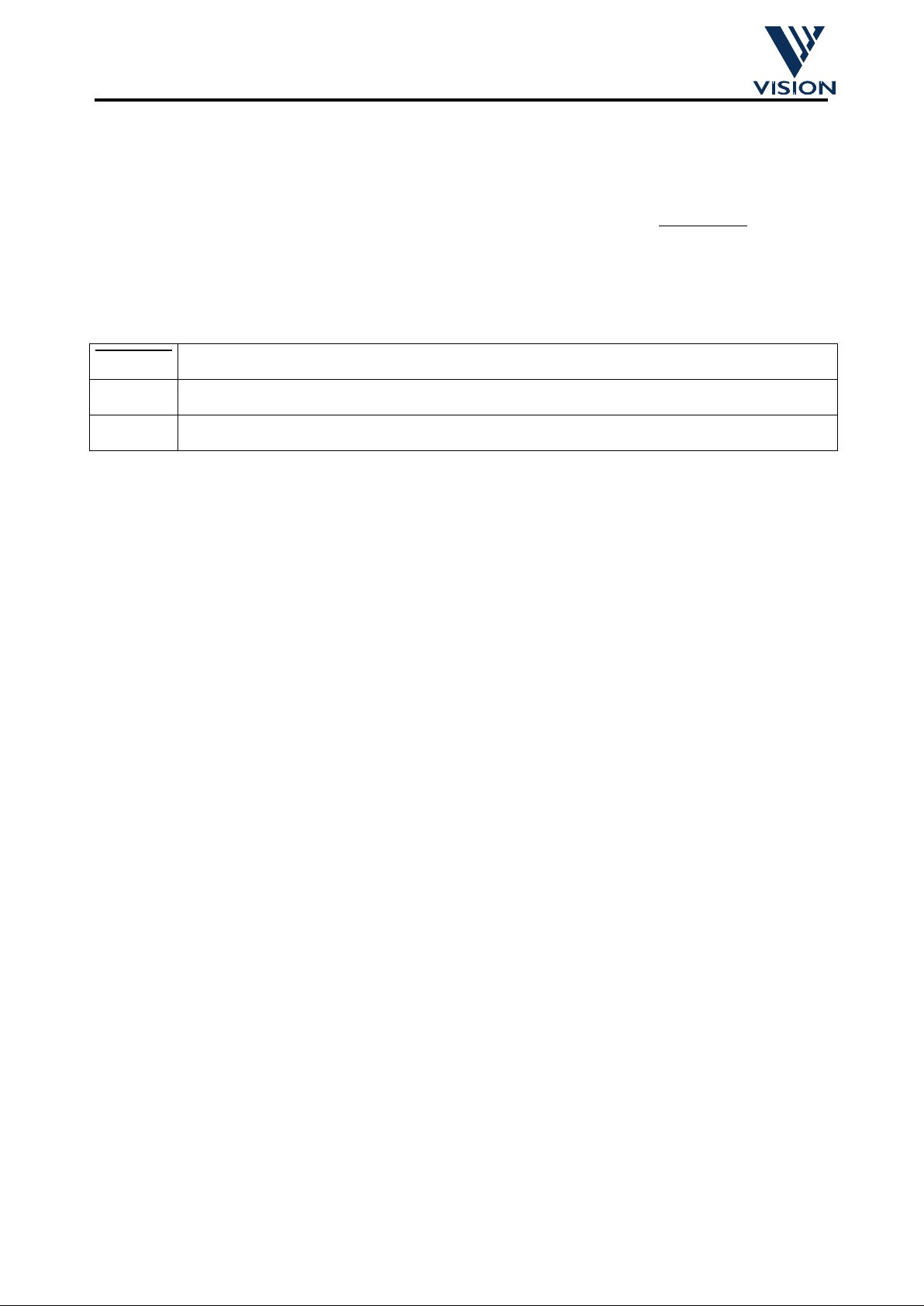
diagram, Figure X.Y, shows the activity that occurs on the parallel port co ntrol and status lines
durin
g
a command transfer to CPiA, via a Forward ECP Mode transfer. NOTE - The actual data is carried on
the 8 data lines, which are not shown on the dia
g
ram.
ID_SELECT Returned Device ID
1
(
default
)
MFG:VLSI Vision Ltd;MDL:PPC2 Camera;CMD:CPIA_1-20;CLS:MEDIA;DES:Parallel Port Camera;
0
MFG:VLSI Vision Ltd;MDL:DUAL-B Camera;CMD:CPIA_1-20;CLS:MEDIA;DES:USB / Parallel Port Camera;
Page 27
V:\apps\cpia\docs\cpia datasheet\cpia_datasheet4.fm
02/07/98 27
Colour Processor Interface ASIC
Commercial In Confidence
Figure 2.9 : Typical Forward ECP Command Transfer to CPiA
The dia
g
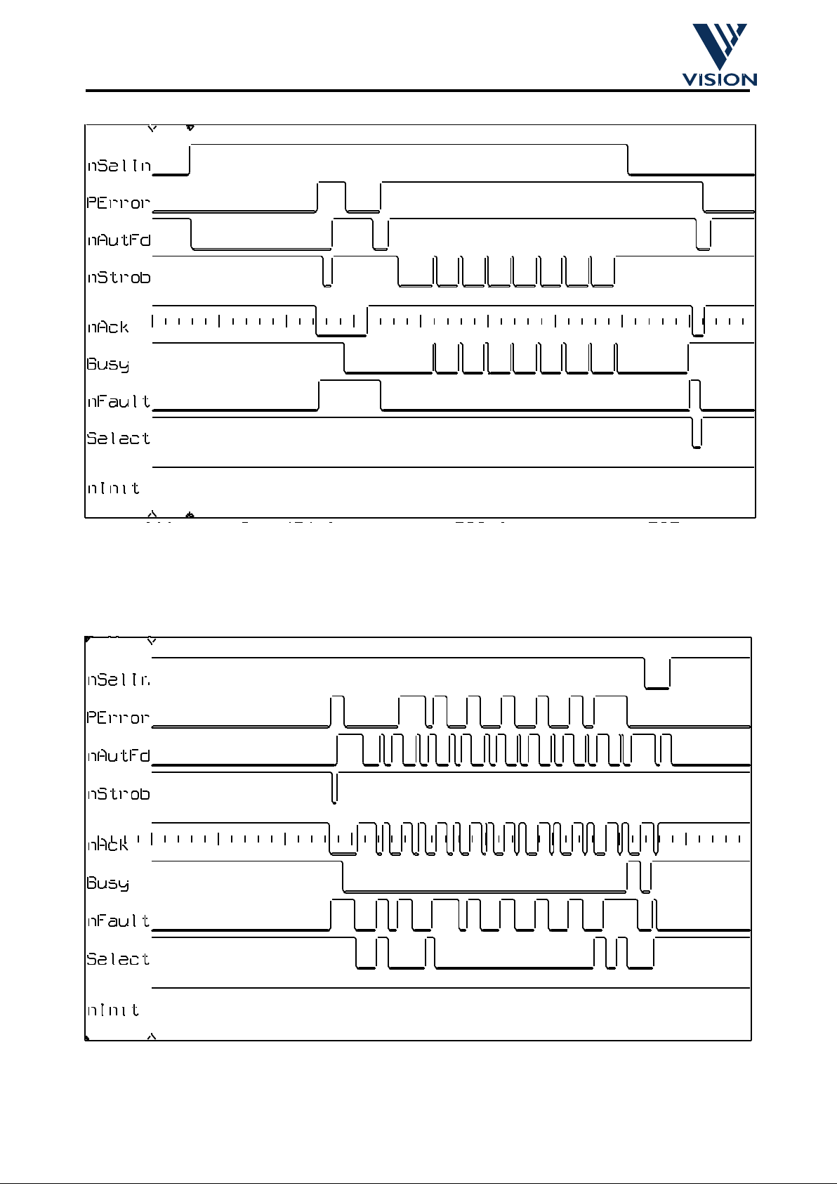
ram below, Figure X.Y, sh ows t he ac tiv i ty that occurs on parall el port control an d st atus lines durin
g
the return of status information to the host via a Nibble Mode transfer. In this transfer mode the actual data is
carried on the PError, nAutoFd, nAck, Select lines.
Figure 2.10 : Reverse Nibble Status Transfer to Host
50 µs Div
100 µs Div
Page 28
V:\apps\cpia\docs\cpia datasheet\cpia_datasheet4.fm
02/07/98 28
Colour Processor Interface ASIC
Commercial In Confidence
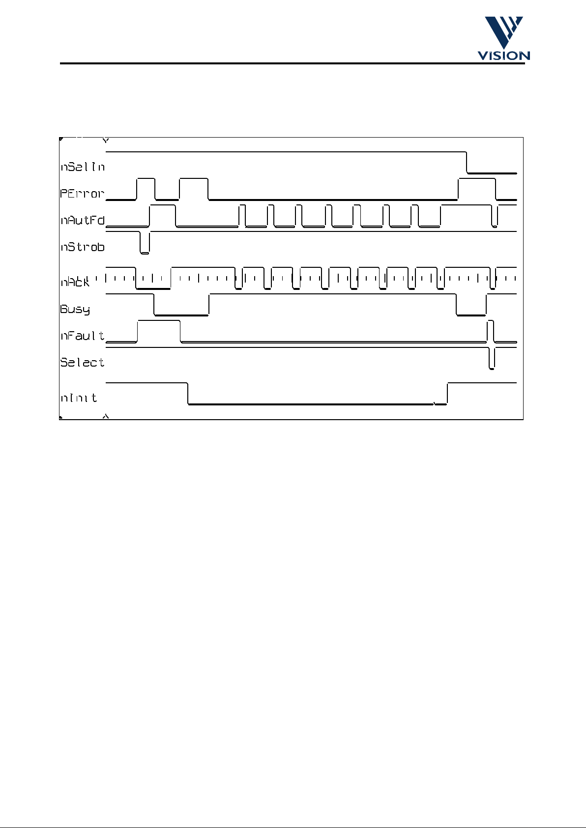
The diagram below, Figure X.Y, sh ows t he ac tiv i ty that occurs on parall el port control an d st atus lines durin
g
the return of status informa tion to the host via a Reverse ECP Mode transfer. NOTE - The actual data is
carried on the 8 data lines, which are not shown on the dia
g
ram.
Figure 2.11 : Typical Reverse ECP Status Transfer to Host
50 µs Div
Page 29
V:\apps\cpia\docs\cpia datasheet\cpia_datasheet4.fm
02/07/98 29
Colour Processor Interface ASIC
Commercial In Confidence
2.2.5.12 Image Stream Transfers
Transfers of image stream data are distinguished from those of the command and status data by the use of a
sli
g
htly different negotiation phase preceeding the transfer. Image stream transfers operates only in the
reverse direction i.e. CPiA to host.
All ima
g
e stream transfer s are preceeded by a 1284 negotiation sequence which sets the "extensib lity link
re
q
uest" bit within the first Extensibility Request Value. The subsequent Extensiblity Request Value then
determines which of two possible transfer modes will be used to transfered the data. Ima
g
e Stream transfers
are terminated with the standard 1284 termination se
q
uence.
The protocol used to transfe r the data depends on the capabilites of the host. If it has an ECP par allel port
then the standa rd ECP b
y
te level protocol is used. Howeve r, if it has a bi-directional, or 4 bit port, then a
modified form of the 128 4 Nibbl e mode t rans fer is us ed. Thi s modifie d form , refered to her eafter as a
Nibble
Stream mode
, is used in preference to th e standard nibble mode to improve the maximum tr ansfer rate.
Nibble Stream mode differs from standard Nibble mode b
y
the fact that both the rising and falling edges of the
nAutoFd si
g
nal are used to clock data.
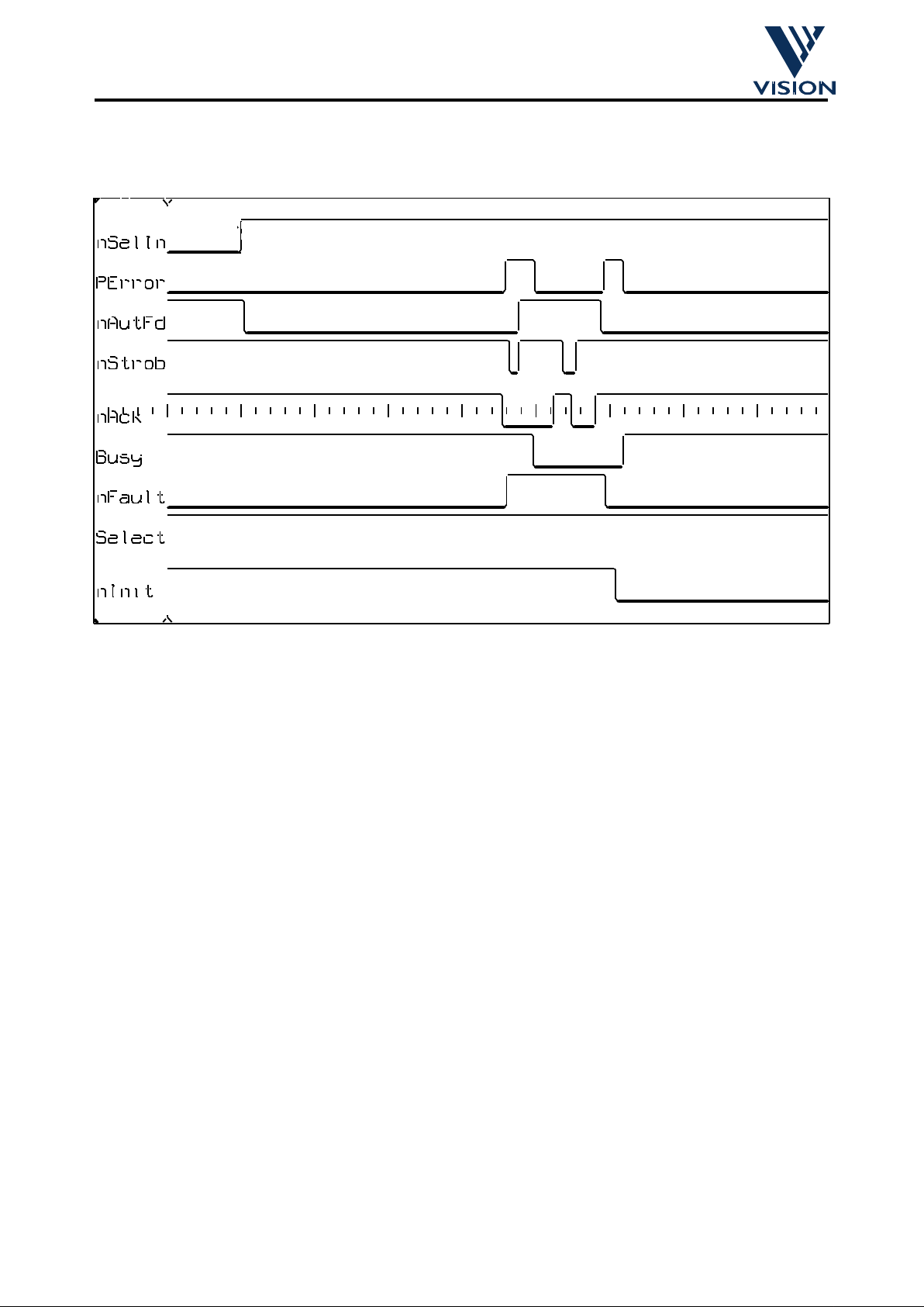
The dia
g
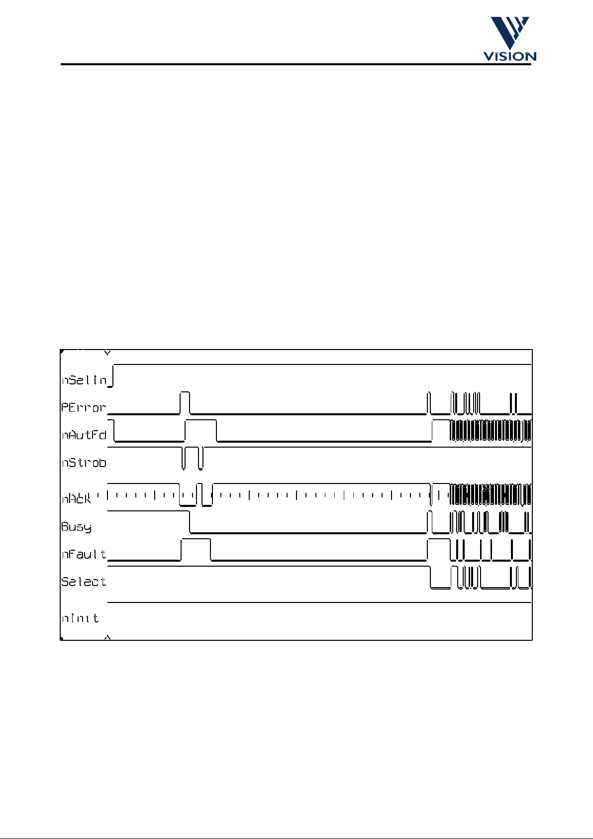
ram below shows the negotiation sequence that proceed s a Nibbl e Stream Mode transfer, and the
start of of the actual ima
g
e data transfer.
NOTE - Re
q
uests by the host for Nibble Stream or ECP Stream mod e transfers can be easily disguished
from standard Nibble Mode and ECP ne
g
otiations by the double nStrobe low p ulses that occur during the
ne
g
otiation phase.
Figure 2.13 : Typical Nibble Stream Negotiation
100 µs Div
Page 30
V:\apps\cpia\docs\cpia datasheet\cpia_datasheet4.fm
02/07/98 30
Colour Processor Interface ASIC
Commercial In Confidence
The diagram below shows the negotiation sequence that proceeds a EC P Stream Mode trans fer, no actual
b
y
tes are shown being transfered.
Figure 2.14 : Typical ECP Stream Negotiation
Notes on Image Stream Transfers
CPiA produces a low
g
oing pulse, of approxi mately 200
µs
, on the nAck line when image stream data is
available to upload . If the host dr iver can use thi s pulse to tri
gg
er a parallel port interrupt ser vice routine to
start the the ima
g
e transfer process.
When the device is sen din
g
compressed image stream to the host the am ount of data to be sent for each
frame can var
y
, depending on the compression ratio achieved . So that the h ost can detect th e end of vali d
data the device inserts a stream of
0xFF
values into the image stream after the host reads past the end the
valid ima
g
e data. As a sequence of four 0xFF values wi ll never occu r within a vali d frame of image data the
host can use this to simpl
y
detect the end of the image data, without having to decompress the image.
The host driver checks the inter
g
rity of the image data stream before it is decoded, if any corruption is
detected the frame is discarded and another uploaded.
If, while uploadin
g
uncompressed images, the transfer of data is monitored via an osciliscope, or logic
anal
y
ser, it will be seen there are regular short pauses in th e transfer, in the order of 200µs to 2ms each.
These are caused b
y
the host driver suspending the transfer while it copies data out of it’s tem porary buffer
into th e ta r
g
et frame buffer.
50 µs Div
Page 31
V:\apps\cpia\docs\cpia datasheet\cpia_datasheet4.fm
02/07/98 31
Colour Processor Interface ASIC
Commercial In Confidence
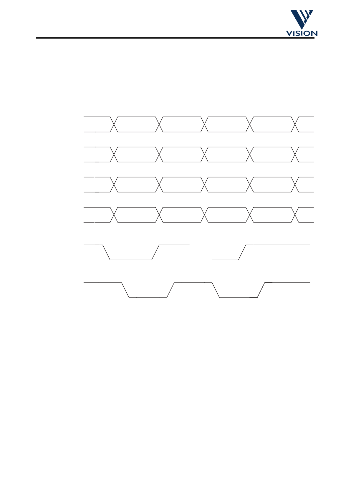
Details of Nibble Stream Mode Protocol
The fi
g
ure below shows the details of the Nibble Stream Protocol. It shows two succesive bytes, A and B, bei n
g
transfered.
The host re
q
uests a byte bysetting nAutoFd to LO. CPiA wi ll the n pr esent the lower nibble of th e byte on the
4 status lines. It then sets nAck LO to si
g
nify that the d at a is r eady. nAutoFd going HI causes the upper nibble
to be placed on the status lines and nAck is then taken HI to si
g
nify the data is ready for the host to read.
Figure 2.15 : Nibble Stream Mode Protocol
2.2.5.16 Pass-Through Mode
• The CPiA device includes support for a parallel port pass-through mode of operation to allow another
parallel port device, e.
g
. a printer, to be daisy chained from a CPiA-based camera.
• The Windows 95/98 device driver supplied b
y
VLSI Vision Ltd does not yet support his feature and so
onl
y
a brief description of the operation of this mode will be given here.
• Please contact Vision for more information.
Description of Pass-Through Mode Operation
The host can instruct the CPiA to enter pass-th rou
g
h mode by sending it a
GotoPassThrough
command. All
host control si
g
nals will then be echo ed to the pass-through port and status signals from the pass-thr ough
port will be echoed back to th e host . In this mo de the hos t has un restricted a ccess the pass-t hrou
g
h device
and ma
y
use it as if the CPiA-based camera was not attached. While in this mode the CPiA will not attempt to
initiate communications with the host, or in an
yway
interfere with the host to pass-through device
communication that ma
y
be taking place.
When the host re
q
uires to communicate with CPiA, it must switch CPiA out of pass-through mode by sendin
g
it a VPP(Visio n P as st hr ough Packet) , which has a simila r struct ure and signaling method as that defin ed in
the IEEE 1284 .3 Draft Specification. This VPP packet is sent usin
g
only the 8 data lines without any strobin
g
or acknowledging on the control or status lines, this en su re s th at th e pa ss - thr ough device will not resp ond to
it.
nAck
nAutoFd
Data bit A:0 Data bit B:0Data bit A:4
nFault
Data bit A:3 Data bit B:3Data bit A:7
Busy
Data bit A:2 Data bit B:2Data bit A:6
PError
Data bit A:1 Data bit B:1Data bit A:5
Select
Data bit B:5
Data bit B:4
Data bit B:6
Data bit B:7
P
P
P
P
P
H
Page 32
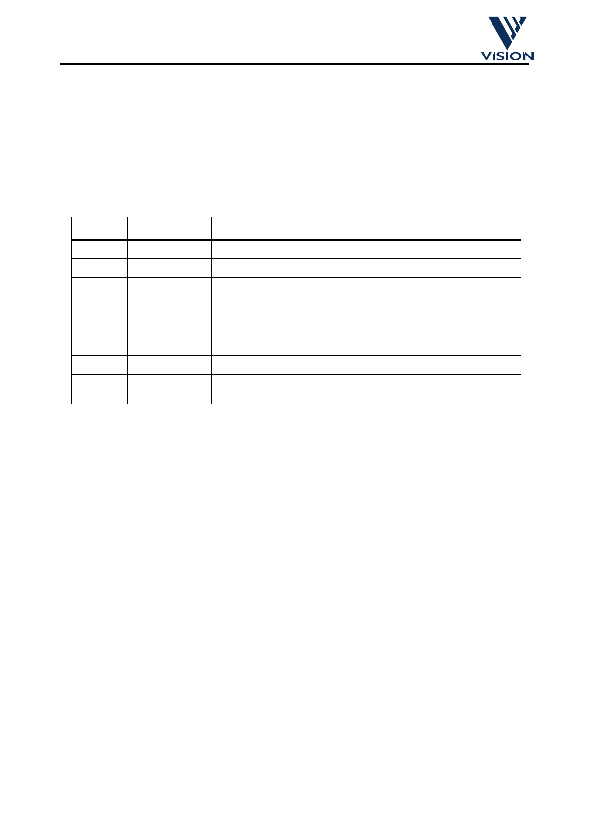
V:\apps\cpia\docs\cpia datasheet\cpia_datasheet4.fm
02/07/98 32
Colour Processor Interface ASIC
Commercial In Confidence
When CPiA switc hes f rom p ass-thr ough into manual mod e it l ocks th e stat e of the pass -through port control
si
g
nals and preven ts th e pass- th ro ugh status signals from being echoed back to the host. The host can now
communicate as it wishes with CPiA without the pass-throu
g
h device being aware of any activity on the
parallel port.
2.2.5.17 IEEE 1284 Mode Handshake Values
The following table shows the timing values of the parall el port interface in terms of the signal transitions
defined in the IEEE Std 1284 fi
g
ures 3 through 23.
Figure 2.18 : IEEE 1284 Mode Handshake Values
Notes:
1 - A delay of more than this period during a Command/Status transfer can cause the watchdog reset circuitry on
CPiA to time out and
g
enerate a system reset.
2 - Normall
y
10ms, however, certain commands being issued to CPiA can caused this to increase to 40ms
3 - As an ECP Forward Channel stall co ndition will never be
g
enerated by CPiA, the Host Transfer Recovery hand-
shake is not supported.
Time Minimum Maximum Description
T
H
0 0.5 s(note 1
)
Host response time
T 0 Infinite response time
T
L
70 ns 10 ms (note 2
)
Peripheral response time
T
R
70 ns Peripheral response time
(
ECP Mode only
)
T
S
(
note 3
)
Host recovery time
(
ECP Mode onl
y)
T
P
0.5 µs Minimum setup or pulse width
T
D
0 Minimum data setup time
(
ECP Mode onl
y)
Page 33
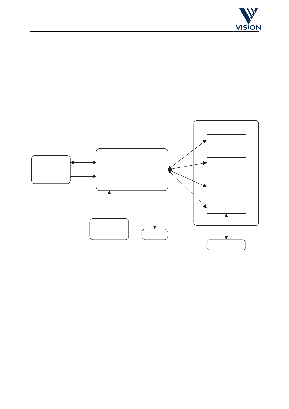
V:\apps\cpia\docs\cpia datasheet\cpia_datasheet4.fm
02/07/98 33
Colour Processor Interface ASIC
Commercial In Confidence
2.2.6 Control Processor
2.2.6.19 Control Processor Interfaces
As shown in figure 2.16 below, the Control Processor uses five main interfaces to control the operation of the
CPiA device:
• VP Control Re
g
isters
• VP Frame Start Interrupt
• VC Control Re
g
isters i.e. PP, USB interfaces, Compression Control and DRAM Interface
• USB_BANDWIDTH
, ID_SELECT and DEBUG input pins
• UART serial comms
(
debug output onl
y)
Figure 2.20 : Control Processor Interfaces
The VP Control Re
g
isters are used to control the colour processing of the raw sensor dat a. Colour channe l
g
ains, colour satur ation and con trast value s are all appli ed by the VP module. Also, commun ications to th e
sensor, for control of exposure time and
g
ain, are done via the VP module.
The VP Frame Start interrupt is used to tri
gg
er Exposure Control and Auto White Balance algorithms that run
on the Control Processor.
The VC Re
g
isters are used to control the host interfaces (both Parallel Port and USB) and the image capture
/ compression / upload processes. In addition access to the DRAM, used to store the frameheader, and
durin
g
self-test mode, is via the VC regisiters. Control of trans itions bet ween the system power states of the
camera is preformed via VC re
g
isters that access the Power Managment module.
The USB_BANDWIDTH,
ID_SELECT and DEBUG input s go directly to port pins on the embedded Contro l
Processor core and modif
y
the several aspec ts of the camera behaviour. In normal o peration these three
inputs should be left unconnected
(
internally pulled up).
The USB_BANDWIDTH
input can be used to se lect a n alter nate set of isoc hronous bandwid ths for th e USB
interface. See the USB Interface section of this document for more details.
The ID_SELECT
input is used to selec t a Device ID (Parallel Port interface) or Product ID (USB interface
)
that is used for combined USB and Parallel Po rt cameras. If held LO it causes a different 1284 Device ID to
be returned on the parallel port interface, and a different USB Product ID on the USB Interface.
The DEBUG
input if pulled LO will cause the Control Processor to send diagnostic output to the serial UART.
Control ProcessorVideo Proccessor
Parallel Port Interface
USB Interface
Image Capture /
Compression
DRAM Interface
Serial UART
USB_BANDWIDTH
ID_SELECT
DEBUG
Video Compressor
System DRAM
Frame
Start
Interrupt
Control Processor
Page 34

V:\apps\cpia\docs\cpia datasheet\cpia_datasheet4.fm
02/07/98 34
Colour Processor Interface ASIC
Commercial In Confidence
This output consists m ainly of a trace of all comman d and status data that has been receive d/transmitted
over the host parallel port or USB interfaces.
The serial UART Tx si
g
nal is used to output diagnostic information. The Rx input is not used to receive serial
data, but the Control Processor does check it’s state after power up, or reset. If it is LO at this time the Control
Processor enters a continuous Self-test Mode which it will remain in until the next s
y
stem reset.
2.2.6.21 Control Processor Tasks
The Control Processor is responsible for a variety of functions necessary for the operation of the CPIA
device. In brief these functions are:
• Initialisation of VP and VC modules
• Host communications via Parallel Port IEEE 1284 protocol
• Supervision of host USB interface
• Host command execution
•Ima
g
e Capture / Compression Control
• Camera Auto Exposure
• Camera Auto White Balance
• Production s
y
stem selftest diagnostics
•Dia
g
nostic debug output
2.2.6.22 Selftest Diagnostics
If the Serial UART input Rx is p ulled LO when the system is released from res et the Control Proc essor will
enter Self-test Dia
g
nostics Mode. It will c ontinuou sly run a set of system level tests and output the result on
the Serial UART Tx output. The serial format used i s 19200 baud, 8-bit data, no parit
y
, 1 stop bit, no flow
control.
Below is t
y
pical output from the Selftest Mode.
====== CPIA Ver 1- 20 ======
Continuous Selftest ...
1 - VP_EN -------2 - VC_INT -------3 - Host port -------4 - Pass-thru port Fail
5 - USB core --------
6 - VC register -------7 - DRAM access -------8 - VP register -------9 - Frame grab -------10 - VP data --------
It should be noted that several of these s elf-tests w here designed to test system level conn ectivity between
the VP, VC and CP m odules durin
g
the device developm ent phase, and are now effectiv ely obseleted with
the full inter
g
rated CPiA device.
These self-tests do not attem pt to tes t i n an
yway
the connectivity, or correct operation, of the interface to th e
sensor.
VP_EN Test
Tests an internal CPiA control si
g
nal - should never fail.
VC_INT Test
Tests an internal CPiA control si
g
nal - should never fail.
Host Port
Tests for short circuits between si
g
nals on the Host Parallel port. Will fail if the camera is plugged in a host.
Page 35

V:\apps\cpia\docs\cpia datasheet\cpia_datasheet4.fm
02/07/98 35
Colour Processor Interface ASIC
Commercial In Confidence
Pass-thru Port
Tests f or short circuits and open circui ts on the Pass-Throu
g
h Parallel port. Requires a special loop back
connector to do the test, and so will fail if this is not present.
USB Core
Tests that the USB core has been succesfull
y
configured. Does not check actual communications with host. If
the 48MHz Xtal is fault
y
, or starts up too slowly, this is test will fail. Beca use of thi s parallel port only designs
will alwa
y
s show this test as failing.
VC Register Test
Tests internal CPiA control si
g
nals - should never fail.
DRAM Access Test
Checks for corre ct CPi A ac cess t o DRAM . It doe s th is b
y
writing a test pattern to DRAM, and then verifying it.
VP Register Test
Tests internal CPiA control si
g
nals - should never fail.
Frame Grab Te st
Tests internal CPiA control si
g
nals - should never fail.
VP Data Test
Puts VP module into Colour Bar Mode, and captures a test ima
g
e to DRAM. Then verifys the correct data has
been captured. If DRAM Access test fails this test will also fail.
2.2.6.23 Debug output
If the DEBUG input is pulled LO, the Control Processor will output diagnostic information on the Serial UART
TX line. This outpu t consist s primar il
y
of a trace of all the command and st atus data transact ions that occur
over the host parallel port or USB interfaces. It was primaril
y
designed to be of use for developers working on
the host driver software.
The serial format used is 19200 baud, 8-bit data, no parit
y
, 1 stop bit, no flow control.
The followin
g
shows typical output following a system reset and then subsequent commands be ing received
from the host b
y
the camera.
====== CPIA Ver 1-20 ======
Process loop ...
Detected PP i/f
Command = 01 CmdData = 00 00 00 00 DataIn = 01 14 01 00 A2 88 88 85
Command = 03 CmdData = 00 00 00 00 DataIn = 02 00 00 00 00 00 10 00
Command = 04 CmdData = 00 00 00 00
Command = A6 CmdData = 02 00 00 00
NOTE - When the debug output is enabled it significantly slows the handling of commands by the camera,
and thus the framerate acheived on the host will be much reduced.
Page 36
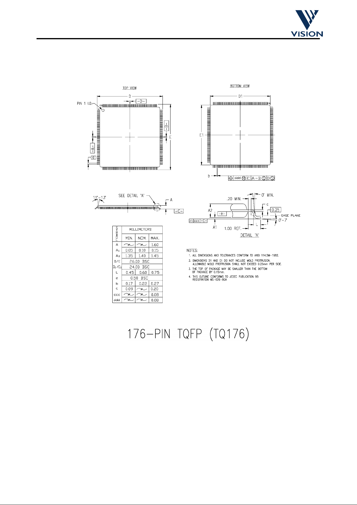
V:\apps\cpia\docs\cpia datasheet\cpia_datasheet4.fm
02/07/98 36
Colour Processor Interface ASIC
Commercial In Confidence
3 Mechanical Information
 Loading...