

Page 1
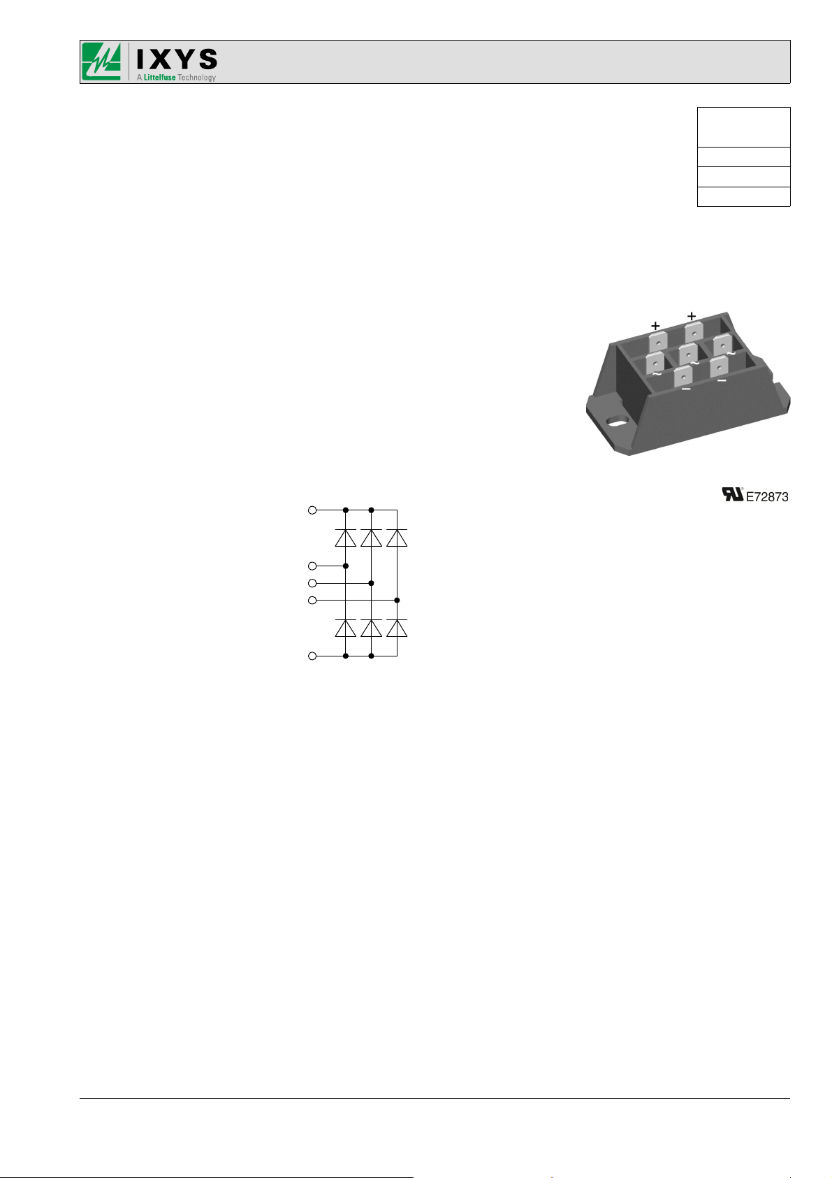
VUO30-14NO3
3~ Rectifier Bridge
Standard Rectifier Module
Part number
VUO30-14NO3
+
D1 D3 D5
3~
Rectifier
V
I 45
DAV
I
RRM
=
=
=
1400
300
V
A
A
~
~
~
D2 D4 D6
-
Features / Advantages: Applications: Package:
● Package with DCB ceramic
● Improved temperature and power cycling
● Planar passivated chips
● Very low forward voltage drop
● Very low leakage current
● Diode for main rectification
● For three phase bridge configurations
● Supplies for DC power equipment
● Input rectifiers for PWM inverter
● Battery DC power supplies
● Field supply for DC motors
● Isolation Voltage: V~
● Industry standard outline
● RoHS compliant
● ¼“ fast-on terminals
● Easy to mount with two screws
● Base plate: DCB ceramic
● Reduced weight
● Advanced power cycling
FO-F
3600
Disclaimer Notice
Information furnished is believed to be accurate and reliable. However, users should independently
evaluate the suitability of and test each product selected for their own applications. Littelfuse products are not designed for,
and may not be used in, all applications. Read complete Disclaimer Notice at
IXYS reserves the right to change limits, conditions and dimensions.
© 2019 IXYS all rights reserved
www.littelfuse.com/disclaimer-electronics.
20191219cData according to IEC 60747and per semiconductor unless otherwise specified
Page 2
VUO30-14NO3
Symbol
Definition
typ.
max.
min.
F
Conditions
Unit
F
Rectifier
Ratings
V
V
I
V
I
V
r
R
R
P
I
I²t
C
R
DAV
F
FSM
RSM
RRM
F
F0
thJC
thCH
tot
J
max. non-repetitive reverse blocking voltage
max. repetitive reverse blocking voltage
reverse current
forward voltage drop
V = V
R
R
I = A
I = AF45
I = A
I = AF45
bridge output current
threshold voltage
slope resistance
for power loss calculation only
thermal resistance junction to case
thermal resistance case to heatsink
total power dissipation
max. forward surge current
T = °C
C
t = 10 ms; (50 Hz), sine T = 45°C
t = 8,3 ms; (60 Hz), sine
t = 10 ms; (50 Hz), sine
t = 8,3 ms; (60 Hz), sine
value for fusing
t = 10 ms; (50 Hz), sine
t = 8,3 ms; (60 Hz), sine
t = 10 ms; (50 Hz), sine
t = 8,3 ms; (60 Hz), sine
junction capacitance
V = V;400 T = 25°Cf = 1 MHz
R
1400
1400
15
15
110
d =rectangular ⅓
T = 25°C
VJ
T = 25°C
VJ
VJ
T = °C
150
VJ
T = 25°C
VJ
125
VJ
T = °C
150
VJ
150
VJ
C
VJ
V = 0 V
R
T = °C
150
VJ
V = 0 V
R
T = 45°C
VJ
V = 0 V
R
T = °C150
VJ
V = 0 V
R
VJ
10
1500
40T = 25°C
1.10
1.38
1.38
45
12.9
60 WT = 25°C
300
325
255
275
450
440
325
315
V
V1400
µA
mA1.5V = V
V
V
V1.01T = °C
V
A
V0.80T = °C
mΩ
2 K/W
K/W0.4
A
A
A
A
A²s
A²s
A²s
A²s
pF
IXYS reserves the right to change limits, conditions and dimensions.
© 2019 IXYS all rights reserved
20191219cData according to IEC 60747and per semiconductor unless otherwise specified
Page 3
VUO30-14NO3
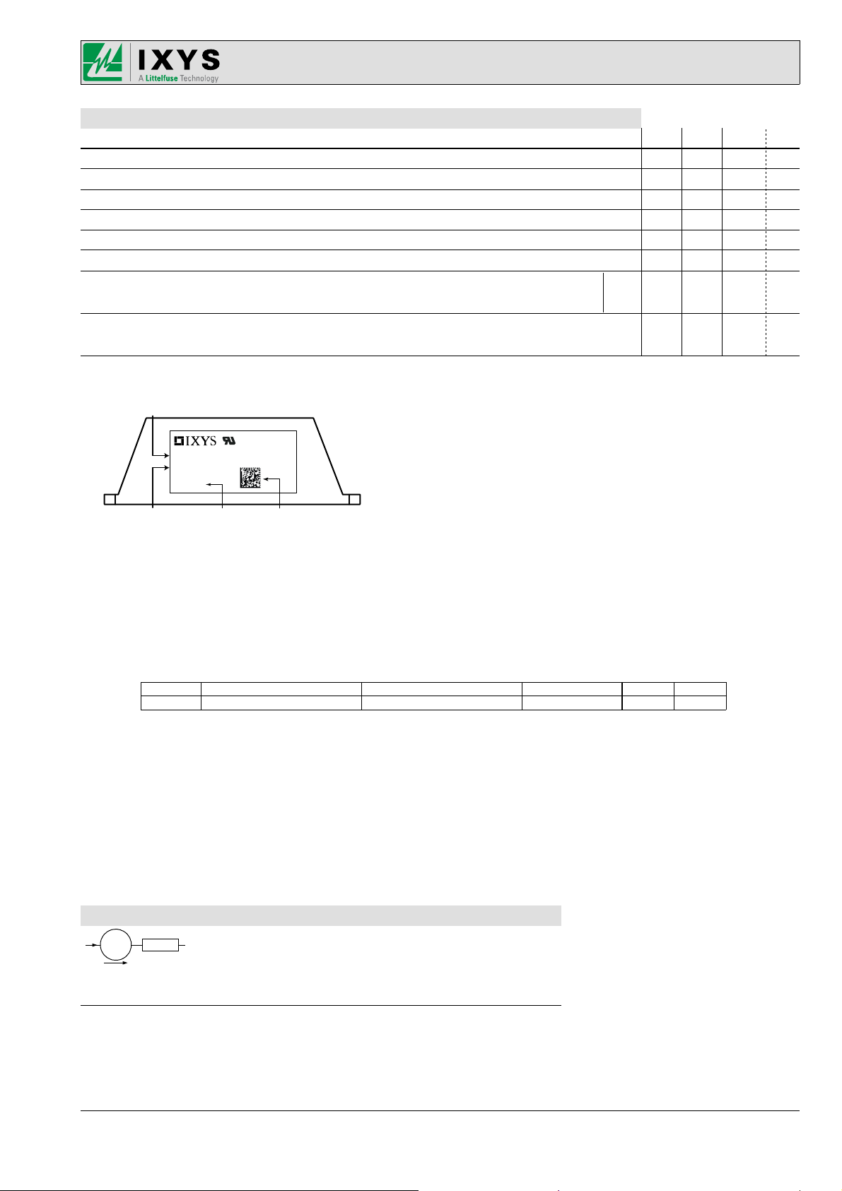
Date Code/Location
Package
Symbol
Definition
typ.
max.
min.
Conditions
Unit
FO-F
I
Ratings
I
RMS
T
VJ
T
op
T
stg
Weight
M
D
d
Spp/App
d
Spb/Apb
V
ISOL
RMS current
per terminal
virtual junction temperature
operation temperature
storage temperature
mounting torque
creepage distance on surface | striking distance through air
isolation voltage
t = 1 second
t = 1 minute
yywwZ
XXXXXXXXX
123456
Part Number
Lot# 2D Barcode
terminal to terminal
terminal to backside
50/60 Hz, RMS; I ≤ 1 mA
ISOL
-40
-40
18.0 6.0
26.0 20.0
3600
3000
100 A
°C150
125-40
°C
°C125
g45
2
Nm2.5
mm
mm
V
V
VUO30-14NO3 425656Box 10VUO30-14NO3Standard
Equivalent Circuits for Simulation
V
V
0 max
R
0 max
R
0
0
threshold voltage
slope resistance *
Rectifier
11.7
* on die level
T =
VJ
150
Delivery Mode Quantity Code No.Ordering Number Marking on ProductOrdering
°C
V0.8
mΩ
IXYS reserves the right to change limits, conditions and dimensions.
© 2019 IXYS all rights reserved
20191219cData according to IEC 60747and per semiconductor unless otherwise specified
Page 4
VUO30-14NO3
5.3
31.6
24.5
6.25
6.25
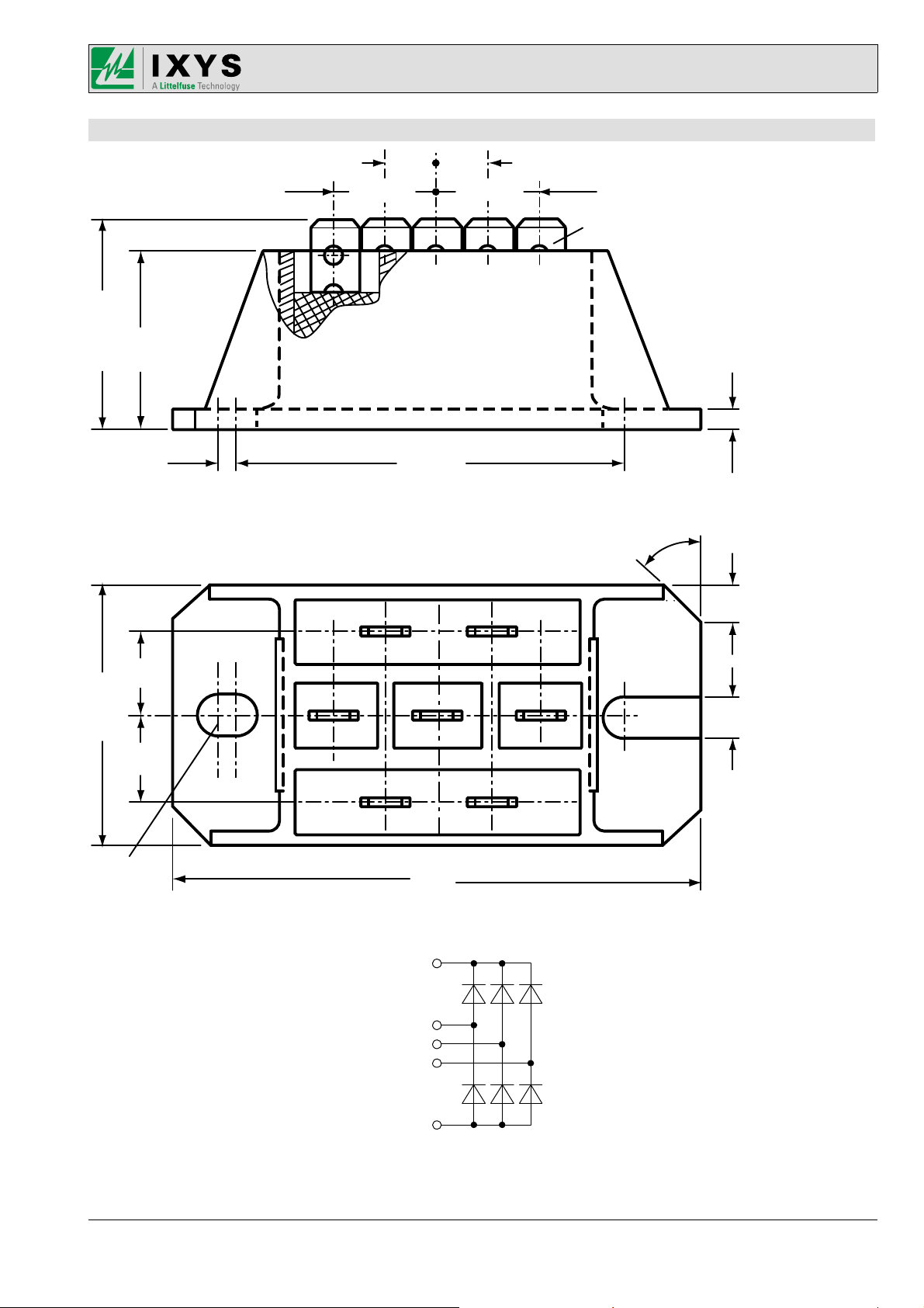
Outlines FO-F
21
1.6
12.5 12.5
48
6.3 x 0.8
4
5
2
°
10
10
x 6.9
1
2
+ +
4
5
~ ~ ~
7
8
_ _
63
+
D1 D3 D5
~
~
~
D2 D4 D6
3
6
4
5.3
9
IXYS reserves the right to change limits, conditions and dimensions.
© 2019 IXYS all rights reserved
-
20191219cData according to IEC 60747and per semiconductor unless otherwise specified
Page 5
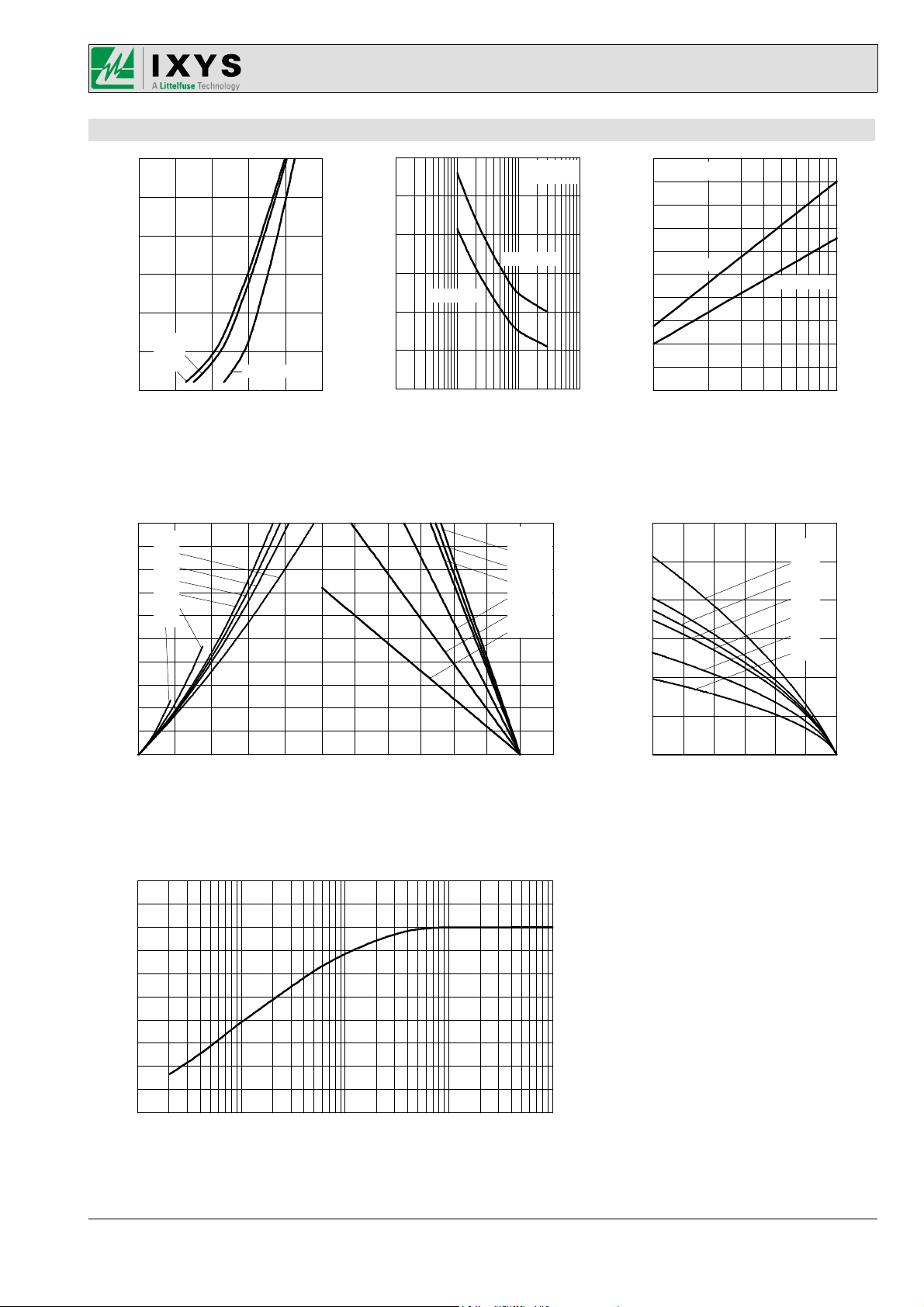
VUO30-14NO3
[
2
50
[
Fig.6Transientthermalimpedanceju
nctionto
case
vs.timeperdiod
e
Rectifier
30
20
I
F
A]
10
TVJ=
125°C
150°C
0
0.4 0.6 0.8 1.0 1.2 1.4
VF[V]
Fig. 1 Forward current vs.
voltage drop per diode
20
DC =
1
0.5
16
0.4
0.33
0.17
12
P
tot
W]
0.08
8
TVJ= 25°C
I
225
200
FSM
175
[A]
TVJ= 150°C
150
125
100
10
-3
10
-2
t [s]
Fig. 2 Surge overload current
vs. time per diode
50 Hz
0.8 x V
TVJ= 45°C
-1
10
R
:
thJA
0.6 KW
0.8 KW
1 KW
2 KW
4 KW
8 KW
RRM
10
0
[A2s]
I
F(AV)M
[A]
500
VR = 0 V
400
I2t
300
TVJ= 45°C
200
100
0
Fig. 3 I2t vs. time per diode
60
50
40
30
20
TVJ= 150°C
011
t [ms]
DC =
1
0.5
0.4
0.33
0.17
0.08
4
0
0 25 50 75 100 125 150 1750 4 8 12 16
I
F(AV)M
[A]
TA [°C]
Fig. 4 Power dissipation vs. forward current
and ambient temperature per diode
2.5
2.0
1.5
Z
thJC
1.0
[K/W]
0.5
0.0
1 10 100 1000 10000
t [ms]
10
0
0 25 50 75 100 125 150
TC[°C]
Fig. 5 Max. forward current vs.
case temperature per diode
Constants for Z
calculation:
thJC
i Rth (K/W) ti(s)
1 0.0607 0.00040
2 0.2030 0.00256
3 0.5005 0.00450
4 0.7030 0.02420
5 0.5328 0.15000
IXYS reserves the right to change limits, conditions and dimensions.
© 2019 IXYS all rights reserved
20191219cData according to IEC 60747and per semiconductor unless otherwise specified
 Loading...