

Page 1
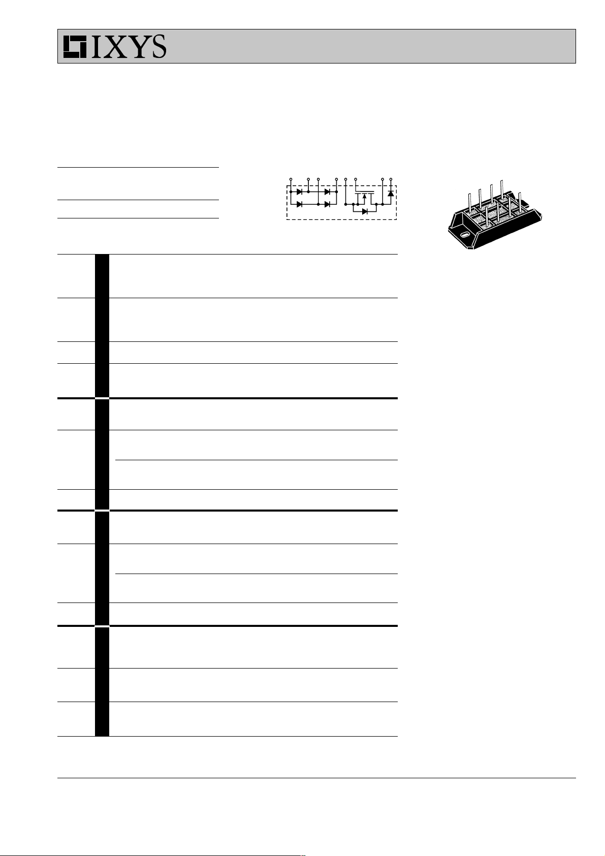
VUM 33-05
Power MOSFET Stage
for Boost Converters
Module for Power Factor Correction
V
RRM (Diode)
V
DSS
Type
513278 46
I
D25
V
R
DSS
DS(on)
= 47 A
= 500 V
= 0.12 W
4
3
2
1
VV
600 500 VUM 33-05N
8
7
Symbol Test Conditions Maximum Ratings
V
DSS
V
DGR
V
GS
I
D
I
D
I
DM
P
D
I
S
I
SM
V
RRM
I
FAV
I
FSM
P TS= 85°C59W
V
RRM
I
dAV
I
FSM
P TS= 85°C50W
T
VJ
T
JM
T
stg
TVJ= 25°C to 150°C 500 V
TVJ= 25°C to 150°C; RGS = 10 kW 500 V
Continuous ±20 V
TS= 85°C33A
TS= 25°C47A
TS= 25°C, tp = ① 130 A
MOSFET
TS= 85°C 310 W
VGS= 0 V, TS = 25°C33A
VGS= 0 V, TS = 25°C, tp = ① 130 A
600 V
Features
●
Package with DCB ceramic base plate
●
Soldering connections for PCB
mounting
●
Isolation voltage 3600 V~
●
Low R
●
Low package inductance for high
HDMOSTM process
DS(on)
speed switching
●
Ultrafast boost diode
●
Kelvin source for easy drive
TS= 85°C, rectangular d = 0.5 33 A
TVJ= 45°C, t = 10 ms (50 Hz) 300 A
t = 8.3 ms (60 Hz) 320 A
T
= 150°C,t = 10 ms (50 Hz) 260 A
VJ
Boost DiodeModule Rectifier Diodes
t = 8.3 ms (60 Hz) 280 A
Applications
●
Power factor pre-conditioner for
SMPS, UPS, battery chargers and
inverters
●
Boost topology for SMPS including
1~ rectifier bridge
●
Power supply for welding equipment
800 V
TS= 85°C, sinus 180° 54 A
Advantages
TVJ= 45°C, t = 10 ms (50 Hz) 300 A
●
t = 8.3 ms (60 Hz) 320 A
TVJ= 150°C,t = 10 ms (50 Hz) 260 A
t = 8.3 ms (60 Hz) 280 A
-40...+150 °C
150 °C
-40...+150 °C
3 functions in one package
●
Output power up to 8 kW
●
No external isolation
●
Easy to mount with two screws
●
Suitable for wave soldering
●
High temperature and power cycling
capability
●
Fits easiliy to all available PFC
controller ICs
6
5
V
ISOL
M
d
Weight 28 g
① Pulse width limited by T
IXYS reserves the right to change limits, test conditions and dimensions.
50/60 Hz t = 1 min 3000 V~
I
£ 1 mA t = 1 s 3600 V~
ISOL
Mounting torque (M5) 2-2.5/18-22 Nm/lb.in.
VJ
© 2000 IXYS All rights reserved
1 - 4
Page 2
VUM 33-05
Symbol Test Conditions Characteristic Values
(TVJ = 25°C, unless otherwise specified)
min. typ. max.
V
V
I
GSS
I
DSS
R
R
g
V
t
d(on)
t
d(off)
C
C
C
Q
R
V
I
R
DSS
GS(th)
DS(on)
Gint
fs
DS
iss
oss
rss
g
thJS
F
VGS = 0 V, ID = 2 mA 500 V
VDS= 20 V, ID = 20 mA 2 5 V
VGS= ±20 V, VDS = 0 V ±500 nA
VDS= 500 V, VGS = 0 V 2 mA
TVJ= 25°C 0.12 W
TVJ= 25°C 1.5 W
VDS= 15 V, IDS = 12 A 30 S
IDS= 24 A, VGS = 0 V 1.5 V
VDS = 250 V, IDS = 12 A, VGS = 10 V
Zgen. = 1 W, L-load
100 ns
220 ns
8.5 nF
= 25 V, f = 1 MHz, VGS = 0 V
V
DS
0.9 nF
0.3 nF
VDS= 250 V, ID = 12 A, VGS = 10 V 350 nC
0.21 K/W
IF= 33 A; TVJ =25°C 1.75 V
TVJ =150°C 1.5 V
VR= 600 V, TVJ =25°C 1.5 mA
VR= 480 V, TVJ =25°C 0.25 mA
TVJ =125°C7mA
350
A
VR= 0.8V
300
250
I
FSM
200
150
100
50
0
0.001 0.01 0.1 1
RRM
TVJ= 45°C
TVJ= 125°C
t
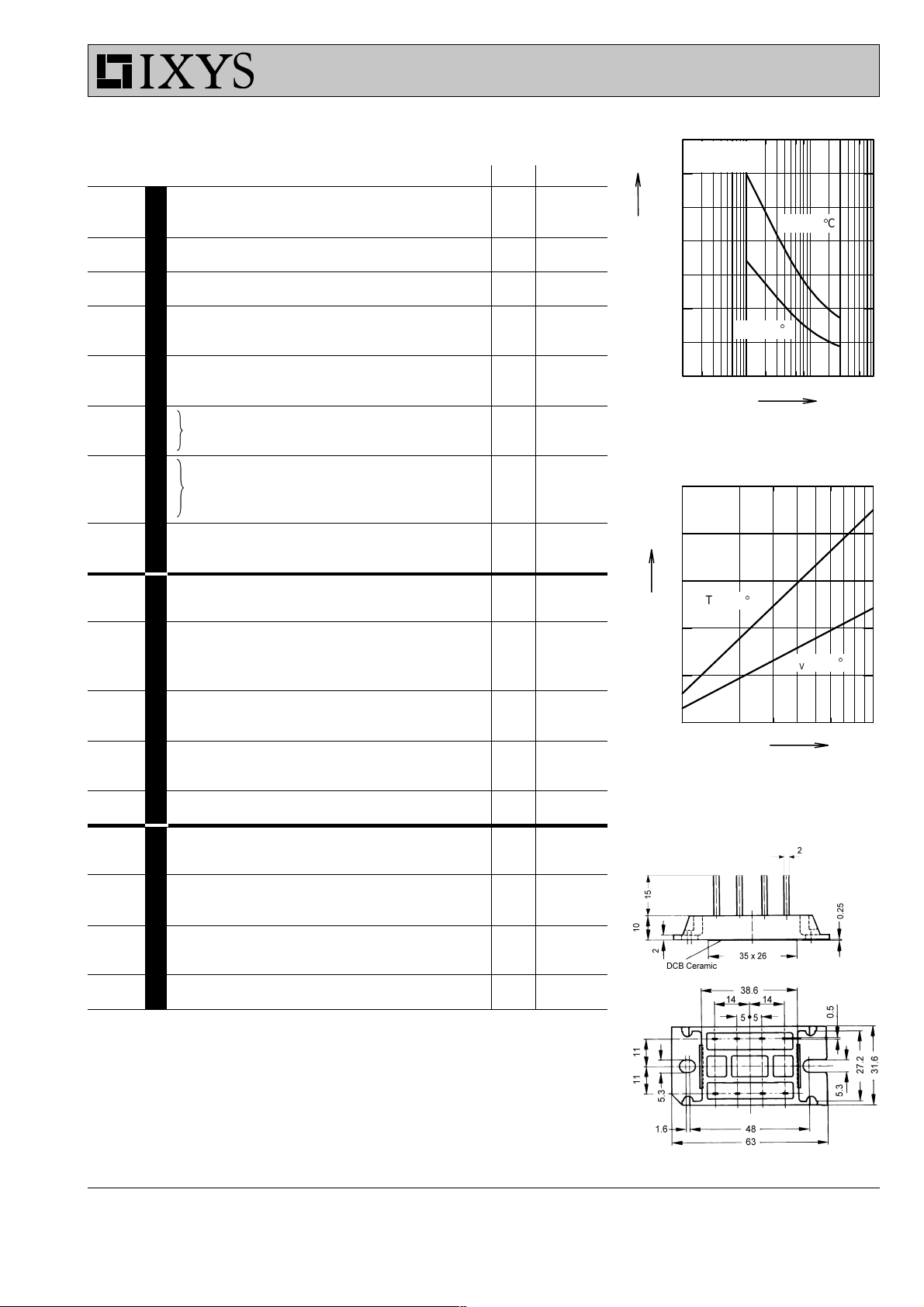
Fig. 1 Non-repetitive peak surge
current (Rectifier Diodes)
500
A2s
400
300
2
I
t
200
100
TVJ= 45°C
TVJ= 125°C
s
V
T0
r
T
I
RM
R
thJS
V
F
I
R
V
T0
r
T
R
thJS
For power-loss calculations only 1.21 V
TVJ= 125°C9mW
IF= 30 A; -diF/dt = 240 A/ms
VR= 350 V, TVJ = 100°C1011A
0
110
t
Fig. 2 I2t for fusing (Rectifier Diodes)
1.1 K/W
IF= 20 A, TVJ =25°C 1.5 V
Dimensions in mm (1 mm = 0.0394")
TVJ =125°C 1.5 V
VR= 800 V TVJ =25°C 0.25 mA
VR= 640 V, TVJ =125°C2mA
For power-loss calculations only 1.18 V
TVJ= 125°C12mW
Rectifier Diodes Boost Diode MOSFET
1.3 K/W
ms
© 2000 IXYS All rights reserved
2 - 4
Page 3
VUM 33-05
80
A
70
60
50
I
D
40
30
VGS= 5 V
20
10
0
0246810
V
DS
10 V
7 V
6 V
V
80
A
70
60
I
50
D
40
TVJ = 25°C
= 125°C
T
VJ
30
20
10
0
234567
V
GS
V
2.5
R
ID=18A
DS(on)
2.0
norm.
1.5
1.0
0.5
0.0
-50 0 50 100 150
T
VJ
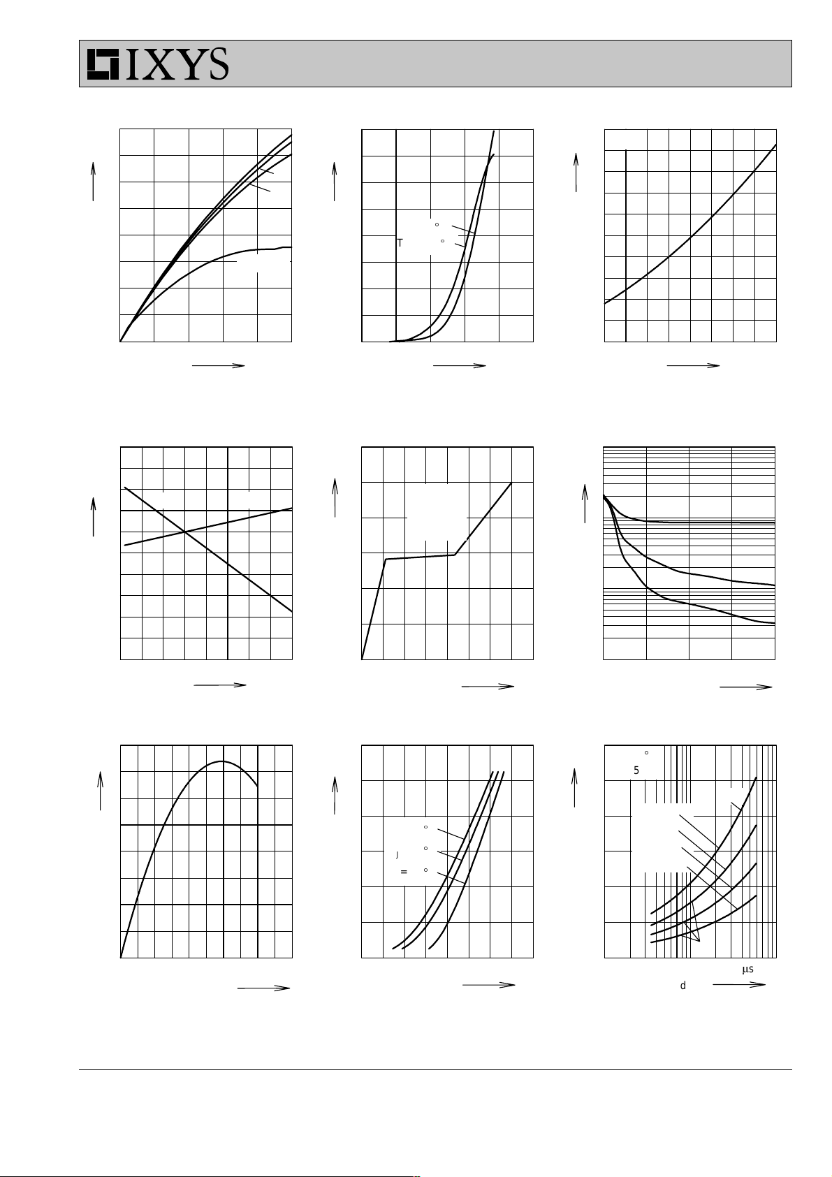
Fig. 3 Typ. output characteristic Fig. 4 Typ. transfer characteristics Fig. 5 Typ. normalized
BV
V
GS(th)
norm.
ID = f (VDS) (MOSFET) ID = f (VGS) (MOSFET) R
1.4
1.2
1.0
0.8
DSS
V
GS(th)
V
DSS
12
V
10
8
V
GS
VDS= 250 V
I
= 18 A
D
I
= 10 mA
G
6
4
100
nF
10
C
1
= f (TVJ) (MOSFET)
DS(on)
C
iss
C
°C
oss
0.6
0.4
-50 0 50 100 150
T
VJ
Fig. 6 Typ. normalized BV
V
= f (TVJ) (MOSFET) characteristics, VGS = f (Qg) (MOSFET) f = 1 MHz (MOSFET)
GS(th)
DSS
80
s
60
g
fs
40
°C
= f (TVJ) Fig. 7 Typ. turn-on gate charge Fig. 8 Typ. capacitances C = f (VDS),
2
0
0 100 200 300 400
Q
g
120
A
100
80
I
F
60
TVJ=150°C
T
=100°C
VJ
T
= 25°C
VJ
40
nC
0.1
0 5 10 15 20
V
DS
3.0
TVJ=100°C
µC
V
= 350 V
R
2.5
2.0
Q
rr
1.5
IF = 37 A
= 74 A
I
F
I
= 37 A
F
= 18.5 A
I
F
1.0
max.
C
rss
V
20
0
0 20406080100
I
D
A
20
0
0.51.01.52.02.5
V
F
V
0.5
-di
F
typ.
A/ms
/dt
0.0
10 100 1000
Fig. 9 Typ. transconductance, Fig. 10 Forward current versus Fig. 11 Recovery charge versus -di
gfs = f (ID) (MOSFET) voltage drop (Boost Diode) (Boost Diode)
/dt
F
© 2000 IXYS All rights reserved
3 - 4
Page 4
VUM 33-05
0.6
µs
0.5
t
rr
TVJ=100°C
V
= 350 V
R
0.4
max.
0.3
0.2
IF = 37 A
I
= 74 A
F
= 37 A
I
F
= 18.5 A
I
F
0.1
I
RM
40
A
30
20
10
TVJ=100°C
= 350 V
V
R
IF = 37 A
= 74 A
I
F
I
= 37 A
F
= 18.5 A
I
F
typ.
max.
1.4
1.2
K
t
1.0
I
RM
0.8
Q
r
0.6
typ.
0
0 100 200 300 400 500 600
-diF/dt
A/ms
0.4
20 40 60 80 100 120 140 160
T
VJ
°C
0.0
0 100 200 300 400 500 600
/dt
-di
F
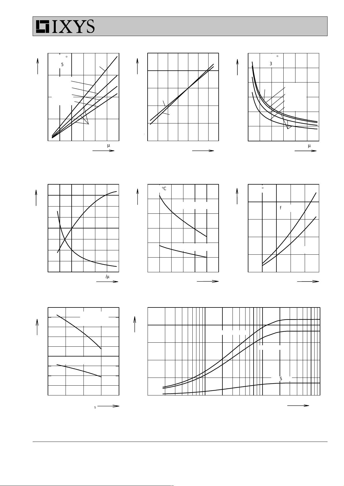
Fig. 12 Peak reverse current versus Fig. 13 Dynamic parameters versus Fig. 14 Recovery time versus
-diF/dt (Boost Diode) junction temperature (Boost Diode) -diF/dt (Boost Diode)
18
V
16
14
V
FR
12
V
FR
10
8
6
t
FR
4
12
TS =85°C
kW
10
P
out
8
Vin = 230 V/50 Hz
10
TS =85°C
kW
8
P
out
f
= 40 kHz
c
6
6
4
4
2
Vin = 115 V/60 Hz
2
fc = 80 kHz
A/ms
2
0 100 200 300 400 500 600
A/ms
diF/dt
0
0 20406080100120
kHz
f
c
0
0 50 100 150 200 250
V
in (RMS)
Fig. 15 Peak forward voltage versus Fig. 16 Output power versus carrier Fig. 17 Output power versus
-diF/dt (Boost Diode) frequency (Module) mains voltage
9
kW
8
fc = 80 kHz
Vin = 230 V/50 Hz
7
6
P
out
5
4
Vin = 115 V/60 Hz
3
2
1
0
40 60 80 100 120
T
S
°C
1.5
VUM 33
K/W
1.2
Z
thJC
Rectifier Diodes
0.9
Boost Diode
0.6
0.3
0.0
0.01 0.1 1 10
MOSFET
s
t
Fig. 18 Output power versus Fig. 19 Transient thermal impedance junction to case for all devices
heatsink temperature (Module)
V
© 2000 IXYS All rights reserved
4 - 4
 Loading...