

Page 1
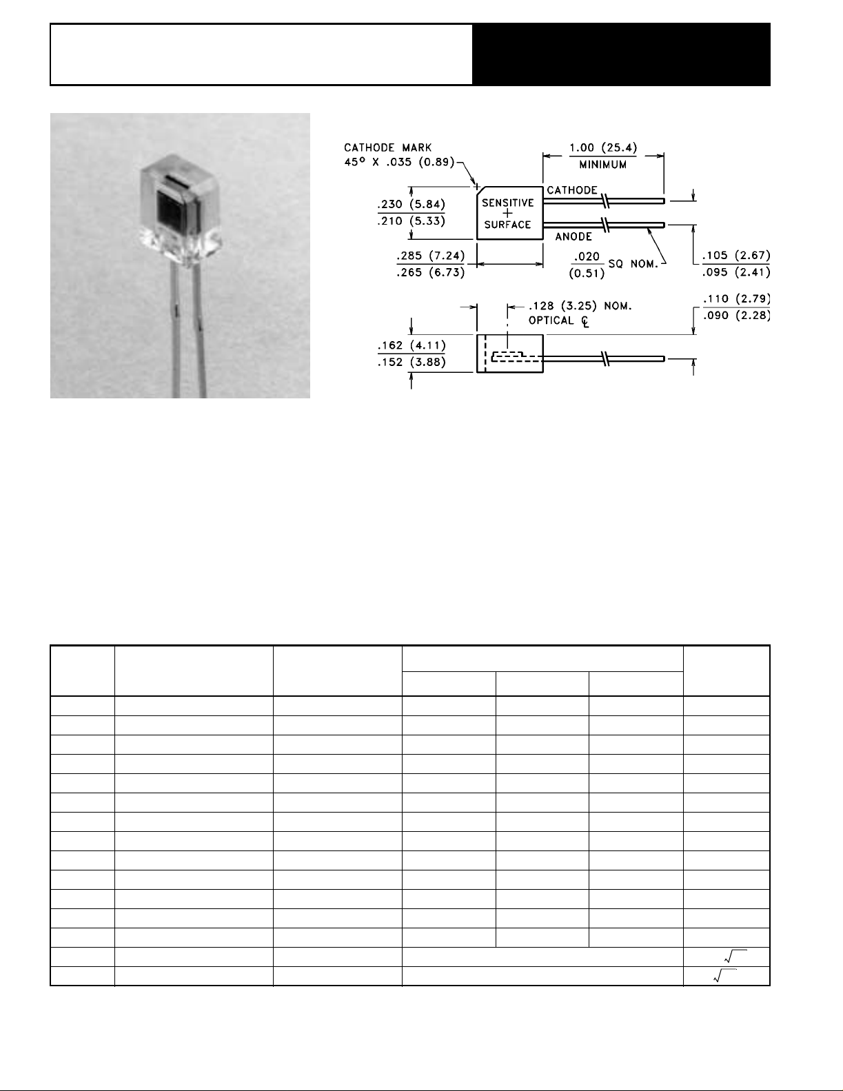
VTP Process Photodiodes VTP100C
PACKAGE DIMENSIONS inch (mm)
CASE 52 FLAT SIDELOO KE R
PRODUCT DESCRIPTION
CHIP ACTIVE AREA: .012 in
2
(7.45 mm2)
Planar silicon photodiode in a molded plastic
sidelooker package. The package material is
clear. These diodes exhibit low dark current and
fas t speed of response.
ABSOLUTE MAXIMUM RATINGS
Storage Temperature: -40°C to 100°C
Operating Temper ature: -40°C to 100°C
ELECTRO-OPTICAL CHARACTERISTICS @ 25°C (See also VTP curves, page 46)
SYMBOL CHARACTERISTIC TEST CONDITIONS
I
TC I
V
TC V
R
Re Responsivity 940 nm .050 A/(W/cm
S
λ
range
V
θ
NEP Noise Equivalent Power 9.0 x 10
Short Circuit Current H = 100 fc, 2850 K 50 70 µA
SC
SCISC
OC
OCVOC
I
D
SH
C
J
R
λ
p
BR
1/2
D* Specific Detectivity 3.0 x 10
Temperature Coefficient 2850 K .20 %/°C
Open Circuit Voltage H = 100 fc, 2850 K 350 mV
Temperature Coefficient 2850 K -2.0 mV/°C
Dark Current H = 0, VR = 10 V 30 nA
Shunt Resistance H = 0, V = 10 mV .25 GΩ
Junction Capacitance H = 0, V = 3 V 50 pF
Sensitivity @ Peak .55 A/W
Spectral Application Range 400 1150 nm
Spectral Response - Peak 925 nm
Breakdown Voltage 30 140 V
Angular Resp. - 50% Resp. Pt. ±70 Degrees
Min. Typ. Max.
VTP100C
-14
(Typ.)
12
(Typ.)
UNITS
WHz⁄
cm Hz
2
)
/ W
PerkinElmer Optoelectronics, 10900 Page Ave., St. Louis, MO 63132 USA Phone: 314-423-4900 Fax: 314-423-3956 Web: www.perkinelmer.com/opto
48
 Loading...