

Page 1
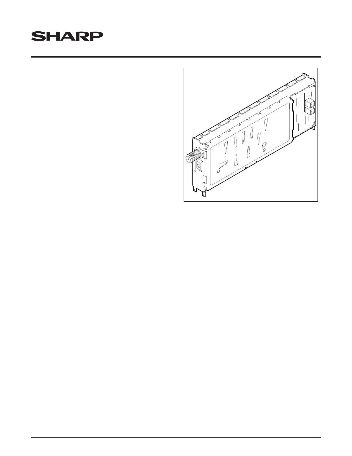
VTBT5UF201
COMB4-1
RF Data Sheet
Combination Tuner/Demodulator
FEATURES
• Receiving Standard: USA
• Receiving Channels:
–VHF Section
– Low Band – Air: 2 to 6 CATV: (A-8) A-5 to B
– High Band – Air: 7 to 13 CATV: C to W + 11
– UHF Section
– Air: 14 to 69
– CATV: W + 12 to W + 84
• Receiving System: USA Standard M-System (NTSC)
• Channel Selection System: PLL Tuning
• Detection System: Dum my Synchronization Detec-
tion System, Intercarrier Sound Receiving System
• Nominal Input Impedance: RF 75 Ω
• Output Load Impedance:
– Video: 1 kΩ
– Audio: 4.7 kΩ
• Intermediate Frequency:
– Picture: 45.75 MHz
– Sound: 41.25 MHz
• Weight: 42 g ±10 g
• Applicable Standards:
– EIA Standard Number 544
– EIA Standard Number 16A
– FCC Standards
– UL Standard
FUNCTIONAL DESCRIPTION
The VTBT5UF201 is a combination tuner and
demodulator in one package. I t is compatible with North
American NTSC television broadcast signals. An internal Phase-Locked Loop circuit performs all of the
required tuning fu nctions. The tuner and demodulator
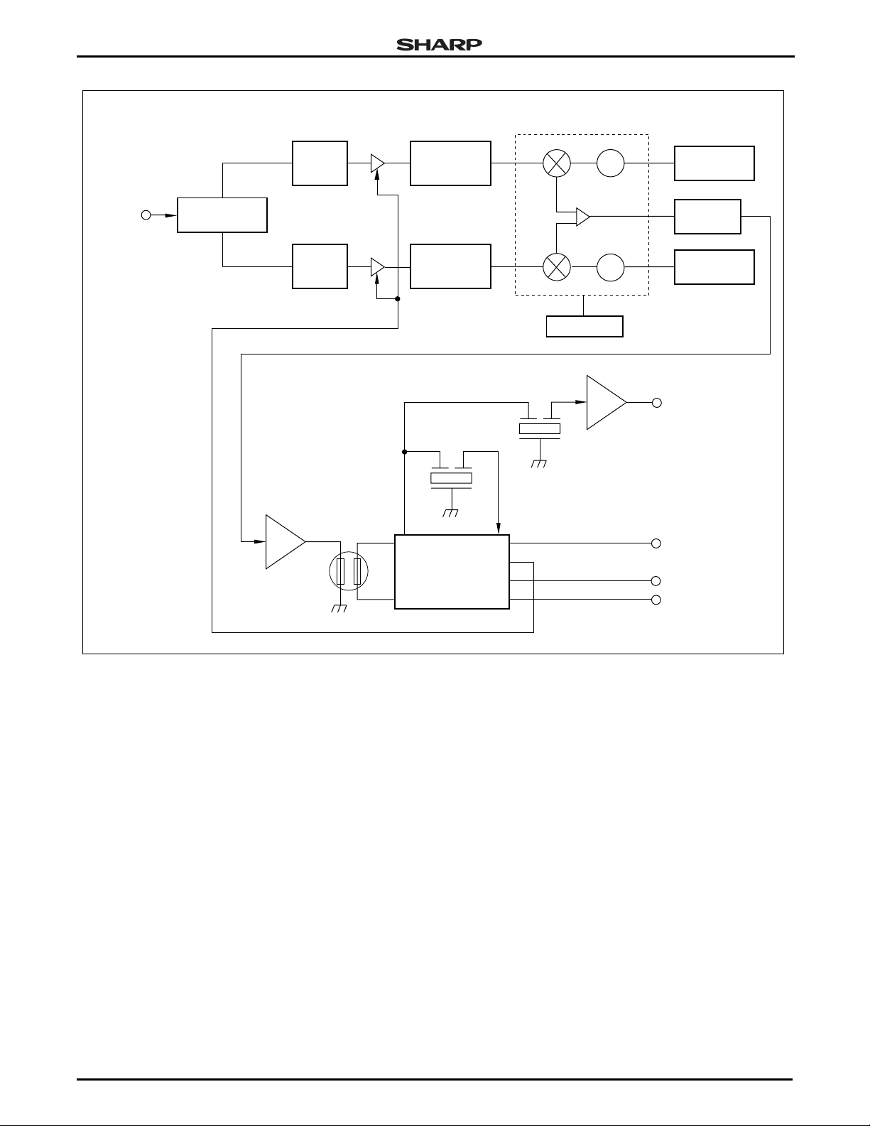
blocks are internally connected. An IF sample port is
provided for monitoring the si gnal level or frequency
characteristics of the recovered IF signal. The RF connector is mounted on the end of the housing so that the
smallest possible area is used on the rear panel of a
final installation. Demodulated audio, video, and AFT
outputs are provided. The AFT Mu te function is available as well. The AGC control line from the demodulator
to the tuner is not accessible to the system designer.
RF Data Sheet 1
Page 2
VTBT5UF201 Combination Tuner/Demodulator
UHF/VHF
IN
U/V SEPARATE
FILTER
UHF
INPUT
TUNING
CIRCUIT
VHF
INPUT
TUNING
CIRCUIT
PRE-AMP
SAW
FILTER
RF
AMP
RF
AMP
DET
OUT
INTERSTAGE
TUNING
CIRCUIT
INTERSTAGE
TUNING
CIRCUIT
SIF
FILTER
DEMODULATOR
IC
U/V ONE CHIP AND IC
MIX
TRAP
SF IN
OSC
IF
AMP
OSC
PLL CIRCUIT
SIF
~
~
VIDEO AMP
RESONANCE
CIRCUIT
IF TUNING
CIRCUIT
RESONANCE
CIRCUIT
VIDEO OUT
AUDIO OUT
AFT OUT
AFT MUTE
Figure 1. VTBT5UF201 Block Diagram
ELECTRICAL CHARACTERISTICS
• Nominal Supply Voltage (TYP.)
– BT: 31 V
–BP: 5 V
–BM: 5 V
• Operating Voltage (TYP.)
– BT: 31 V ±2.0 V
– BP: 5 V ±0.5 V
– BM: 5 V ±0.5 V
– Control: 5 V ±0.2 V
• Breakdown Voltage (MIN.)
– BT: 34 V
–BP: 5.5 V
– BM: 5.5 V
RF AGC
COMB4-6
• Test Conditions (TYP.)
– BT: 31 V
–BP: 5 V
–BM: 5 V
– Ambient Temperature 25°C ±5°C
– Relative Humidity 65% ±10%
• Current Consumption (MAX.)
–BT: 5 mA
– BP: 16 mA
– BM: 150 mA
• Temperature (TYP. )
– Storage -20°C to +70°C
– Operating -10°C to +60°C
2 RF Data Sheet
Page 3
Combination Tuner/Demodulator VTBT5UF201
60
50
40
30
20
88 216
43.5 dB
µ
46 dB
µ
54 dB
µ
960 5000
COMB4-4
RADIATION (dBµ)
FREQUENCY (MHz)
• Noise Figure (UHF AIR)
– Maximum 7 dB (TYP.), 10 dB (MAX.)
–
XΣxi n
⁄
=
– Signal Rising: Trise 1 µs (MIN.)
– Signal Falling: Tfall 1 µs (MIN.)
• Picture Output
– Output Level (CH 10) 1.0 Vp-p (TYP.),
S
Σ
(Tested channels including worst)
2
Xi x
()
n1
()⁄
–
n10*=,=
–
– Shall satisfy the requirements stated in FCC
NF Sampling Plan C (effective January, 1980)
– Noise figure measur ement shall be based on
FCC OST 50 (effective January, 1980)
– XIRS: 7 dB (TYP.), 10 dB (MAX.)
1.0 ±15 Vp-p
–At 1 kΩ termination, fp 70 dBµ, White 100%
– Differential Gain (CH 10) 3% (TYP.), 10% (MAX.)
– fp 90 dBµ, Sterstep 80 IRE
– Differential Phase (CH 10) 3° (TYP.), 10° (MAX.)
– fp 90 dBµ, Sterstep 80 IRE
– S/N ratio 47 dB (TYP.), 43 dB (MIN.)
– fp 70 dBµ, White 100%, 100 kHz to 4.2 MHz fil-
*A representative tuner test shall be conducted on the follow-
NOTE:
ing channels and on the worst channel found CH 14 through CH69:
Ch14, 20, 26, 32, 38, 44, 50, 56, 62, and 69.
• Image Rejection
– At -47 dBM Input
– VHF Air: 70 dB (TYP.), 60 dB (MIN.)
– VHF CATV: 70 dB (TYP.), 60 dB (MIN.)
– UHF: 60 dB (TYP.), 40 dB (MIN.)
• IF Rejection (dB)
– At -47 dBM Input
– VHF Low: 80 dB (TYP.), 55 dB (MIN.)
– VHF High: 90 dB (TYP.), 90 dB (MIN.)
– UHF: 85 dB (TYP.), 60 dB (MIN.)
– At -17 dBM: Input
– VHF Low: 58 dB (TYP.), 50 dB (MIN.)
– VHF High: 63 dB (TYP.), 50 dB (MIN.)
– UHF: 60 dB (TYP.), 50 dB (MIN.)
• Specific Channel Rejection.
– Desirable 54 dBµ input; Undesireable 49 dbµ input.
– CH 6 ← CH A-5: 55 dB (TYP.); 50 dB (MIN.)
– CHP 6 ← CHS6: 55 dB (TYP.); 52 dB (MIN.)
• Band Edge Tuning Margin
– CH 2: -4.0 MHz (TYP.), -1 MHz (MIN.)
– CH B: 3.0 MHz (TYP.), +1 MHZ (MIN.)
– CH C: -4.0 MHz (TYP.), -1 MHz (MIN.)
• Sound Output
• AFT Output
ter, Sctrap On
– Frequency Characteristics (CH 10), fp 70 dBµ,
multi-burst
– 1.0 MHz: -0.3 dB (TYP.), -2 ±0.3 dB
– 2.0 MHz: -0.4 dB (TYP.), -2 ±0.4 dB
– 3.0 MHz: -1.0 dB (TYP.), -1.7 ±0.7 dB
– 3.58 MHz: -2.0 dB (TYP.), -2 ±2 dB
– Synchronize d Ratio (CH 10)
– 28.5% (TYP.), 23.6% to 33.6%
– fp 70 dBµ, SMPTE color bar
– Output Level (CH 10) 245 mVrms (TYP.),
185 mVrms to 315 mVrms
– fp 70 dBµ, SMPTE color bar 87.5% modula-
tion, P/S 6 dB, fs 1 k Hz, si n-c ur ve 60 % mo du-
lation, 75 µs pre-emphasis
– Distortion Rate (CH 10) 1% (TYP.), 4% (MAX.)
– S/N Ratio (CH 10) 53 dB (TYP.), 42 dB (MAX.)
– Frequency Characte ristics (CH 10) 0 dB (TYP.),
0±3 dB
– AM Removal Level (CH 10) 45 dB (TYP.),
35 dB (MAX.)
– Output Voltage 2.5 V (TYP.), 1.75 V to 3.25 V
– Frequency Accuracy 25 kHz (TYP.), 100 kHz (MAX.)
– CH W + 11: 3.0 MHz (TYP.), +1 MHz (MIN.)
– CH W + 12: -5.0 MHz (TYP.), -1.5 MHz (MIN.)
– CH 69: 6.0 MHz (TYP.), 1.0 MHz (MIN.)
• Antenna Terminal Voltage
– Fundamental Wave 40 dBµ (MAX.)
– Higher Harmonic 48 dBµ (MAX.)
• PLL AC Characteristics
– Setting Up Enable: Tsuen 1 µs (MIN.)
– Holding Enable: Thden 1 µs (MIN.)
– Setting Up Data: Tsuda 1 µs (MIN.)
– Holding Data: Thdda 1 µs (MIN.)
– Clock Level High: Thicl 1 µs (MIN.)
– Clock Level Low: Tlocl 1 µs (MIN.)
– Clock Rate: Trate 10 µs (MIN.)
RF Data Sheet 3
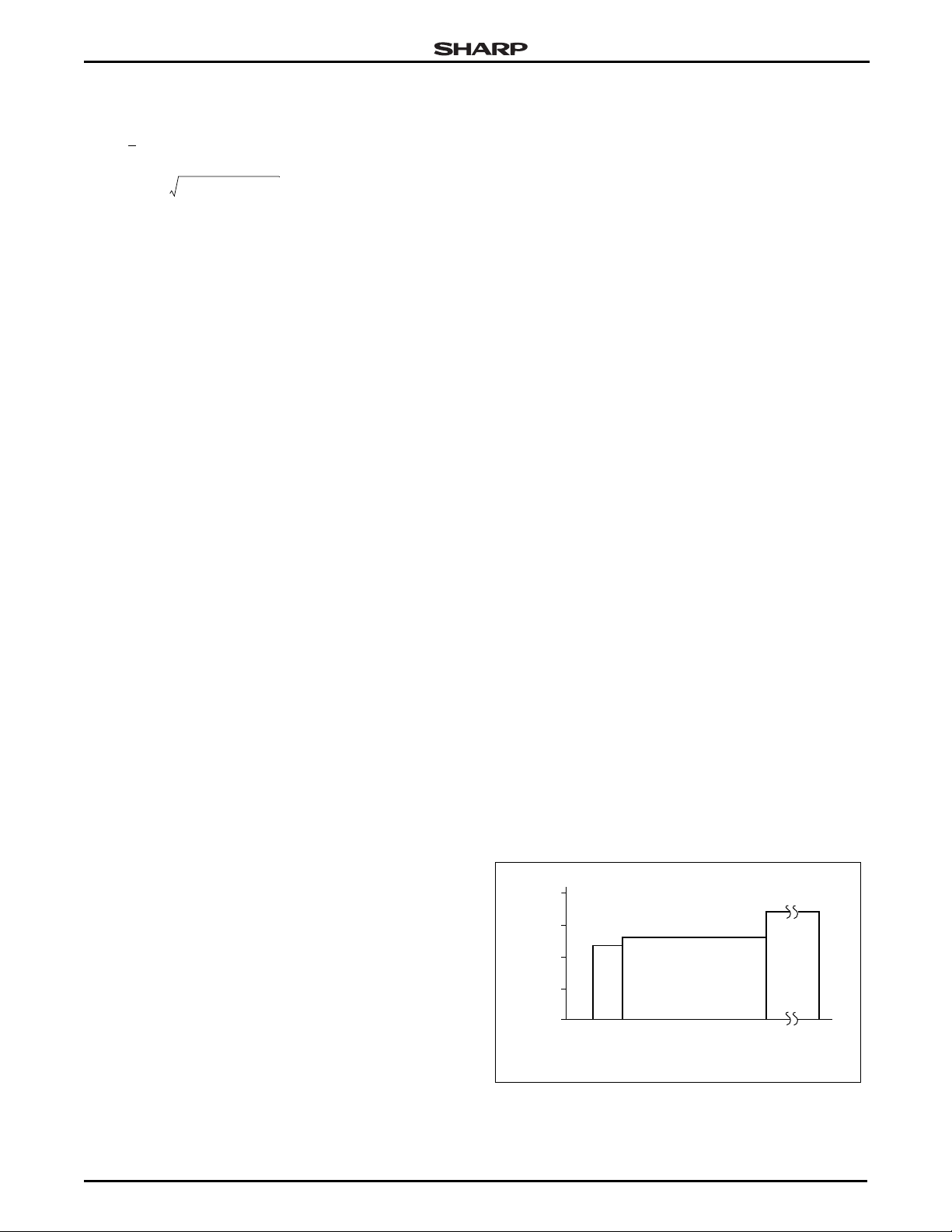
Figure 2. Radiation (3m Method)
Page 4
VTBT5UF201 Combination Tuner/Demodulator
105
95
85
75
DESIRED INPUT LEVEL (dBµ)
65
50
60 70 1009080
UNDESIRED INPUT LEVEL (dBµ)
110
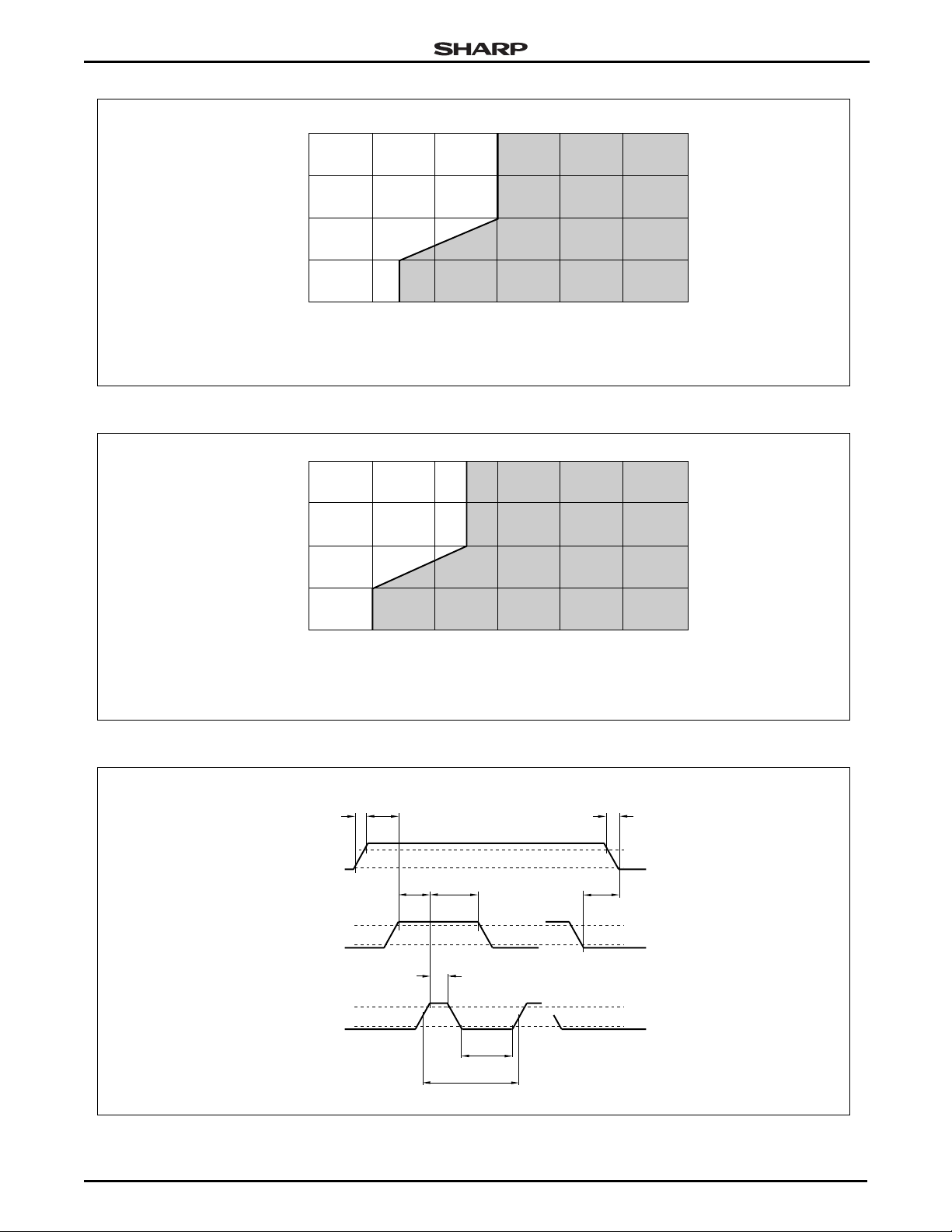
NOTE: Input levels causing 1% cross modulation are shown in shaded area.
Figure 3. Cross Modulation Between Next and Adjacent Channels
105
95
85
75
DESIRED INPUT LEVEL (dBµ)
65
50
60 70 1009080
UNDESIRED INPUT LEVEL (dBµ)
NOTE: Input levels causing 1% cross modulation are shown in shaded area.
Figure 4. Cross Modulation Between Adjacent Channels
t
RISEtSUEN
t
FALL
COMB4-2
110
COMB4-3
t
HDEN
90%
10%
90%
10%
90%
10%
COMB4-5
ENABLE
DATA
CLOCK
t
SUDAtHDDA
t
HIEL
t
RATE
t
LOEL
Figure 5. PLL AC Characteristics
4 RF Data Sheet
Page 5
Combination Tuner/Demodulator VTBT5UF201
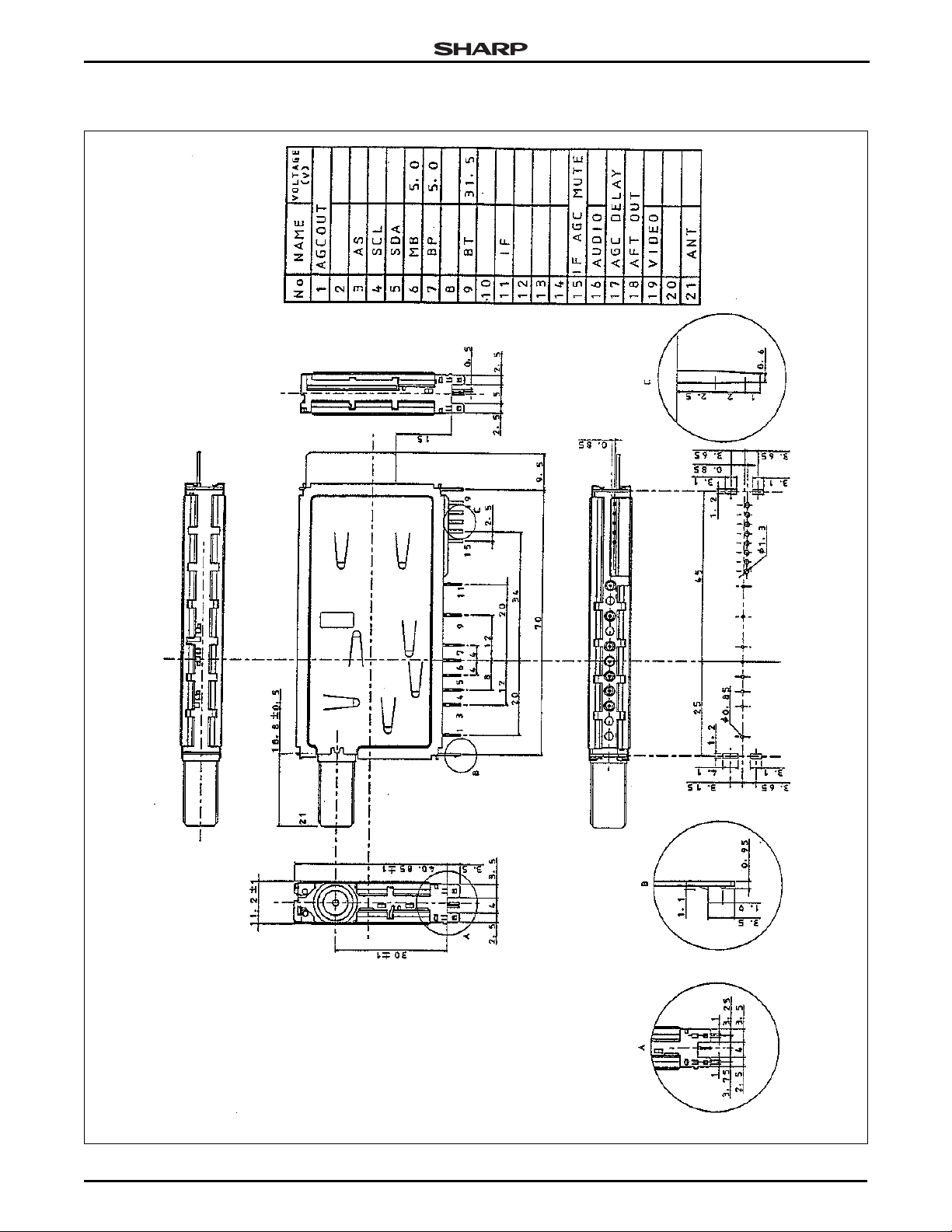
OUTLINE DIMENSIONS
RF Data Sheet 5
Page 6
VTBT5UF201 Combination Tuner/Demodulator
LIFE SUPPORT POLICY
SHARP components should not be used in medical devices with life support functions or in safety equipment (or similiar applications where
component failure would result in loss of life or physical harm) without the written approval of an officer of the SHARP Corporation.
LIMITED WARRANTY
SHARP warrants to its Customer that the Products will be free from defects in material and workmanship under normal use and service for a
period of one year from the date of invoice. Customer's exclusive remedy for breach of this warranty is that SHARP will either (i) repair or
replace, at its option, any Product which fails during the warranty period because of such defect (if Customer promptly reported the failure to
SHARP in writing) or, (ii) if SHARP is unable to repair or replace, refund the purchase price of the Product upon its return to SHARP. This
warranty does not apply to any Product which has been subjected to misuse, abnormal service or handling, or which has been altered or
modified in design or construction, or which has been serviced or repaired by anyone other than Sharp. The warranties set forth herein are in
lieu of, and exclusive of, all other warranties, express or implied. ALL EXPRESS AND IMPLIED WARRANTIES, INCLUDING THE
WARRANTIES OF MERCHANTABILITY, FITNESS FOR USE AND FITNESS FOR A PARTICULAR PURPOSE, ARE SPECIFICALLY
EXCLUDED. In no event will Sharp be liable, or in any way responsible, for any incidental or consequential economic or property damage.
The above warranty is also extended to Customers of Sharp authorized distributors with the following exception: reports of failures of Products
during the warranty period and return of Products that were purchased from an authorized distributor must be made through the distributor.
In case Sharp is unable to repair or replace such Products, refunds will be issued to the distributor in the amount of distributor cost.
SHARP reserves the right to make changes in specifications at any time and without notice. SHARP does not assume any responsibility
for the use of any circuitry described; no circuit patent licenses are implied.
NORTH AMERICA
SHARP Microelectronics
of the Americas
5700 NW Pacific Rim Blvd., M/S 20
Camas, WA 98607, U.S.A.
Phone: (360) 834-2500
Telex: 49608472 (SHARPCAM)
Facsimile: (360) 834-8903
EUROPE
SHARP Electronics (Europe) GmbH
Microelectronics Division
Sonninstraße 3
20097 Hamburg, Germany
Phone: (49) 40 2376-2286
Facsimile: (49) 40 2376-2232
http://www.sharpmed.com
ASIA
SHARP Corporation
Integrated Circuits Group
2613-1 Ichinomoto-Cho
Tenri-City, Nara, 632, Japan
Phone: (07436) 5-1321
Telex: LABOMETA-B J63428
Facsimile: (07436) 5-1532
http://www.sharpsma.com
©1999 by SHARP Corporation Reference Code SMA99023
 Loading...