

Page 1
V
T98521
p
r
3.3V Clock Multi
lie
Applications
•= Low cost general-purpose clock source
General Description
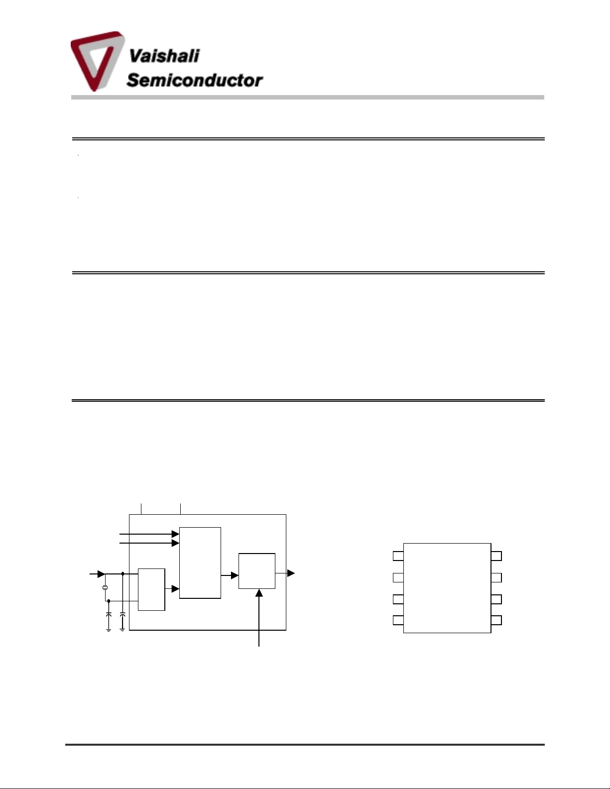
The VT98521 is a 3.3V CMOS, clock multiplier integrated circuit. The device provides an excellent quality
high frequency output clock from a lower frequency crystal or clock input. Tri-level selection inputs S0 and
S1 are used to select any one of eight multipliers, stored in the on-board ROM, and apply it to the input to
produce the desired output, up to 220 MHz. Phase Locked Loop (PLL) technology allows the device to use
an input signal from an inexpensive crystal. When Output Enable (OE) is low, the clock output is in high
impedance state.
The VT98521, when used with an inexpensive crystal, provides a cost-effective clock source for most
electronic systems.
Features
•= Low phase noise
•= Zero ppm multiplication error
•= Input clock frequency 5 - 50 MHz.
•= Input crystal frequency 5 – 27 MHz
•= Output clock frequencies up to 220 MHz.
•= 5V-tolerant inputs and output
•= Fully Compatible with all popular CPUs
•= Duty Cycle - 45/55 up to 160 MHz.
- 40/60 160 MHz to 220 MHz
•= 25mA drive capability at TTL levels
•= High-Z output for board level testing
Figure 1. Functional Block Diagram
Figure 2. Pin Assignment
VDD
S0
S1
Clock or
Xtal
input
2002-02-25 Page 1 MDST-0017-02
X1/ICLK
X2
Optional
caps
Vaishali Semiconductor 747 Camden Avenue, Suite C Campbell CA 95008 Ph. 408.377.6060 Fax 408.377.6063
Xtal.
Osc.
GND
PLL
Clock
Multiplier
&
ROM
Output
Buffer
Output Enable
www.vaishali.com
CLK
X1/ICLK
VDD
GND
S1
8-pin SOIC/MSOP
1
2
3
4
8
7
6
5
X2
OE
S0
CLK
Page 2
VT98521
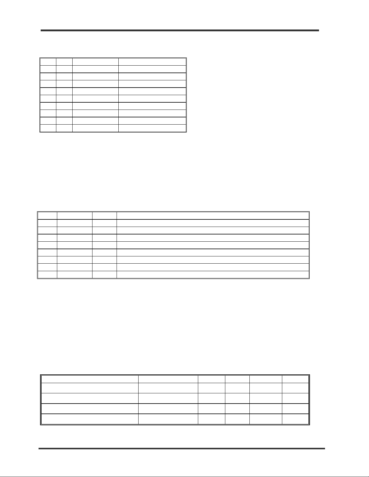
Table 1. Clock Output Table
S1 S0 CLK Minimum Input
0 0 4 x input See table 6
0 M 5.3125 x input 20 MHz
0 1 5 x input See table 6
M 0 6.25 x input 4 MHz
M M Test*
M 1 3.125 x input 8 MHz
1 0 6 x input See table 6
1 M 3 x input See table 6
1 1 8 x input See table 6
0 = Connect to ground.
1 = Connect directly to VDD
M = Leave unconnected (floating)
* = For Vaishali internal test purposes only
Table 2. Pin Description
No. Name Type Description
1 X1/ICLK I Xtal connection or clock input.
2 VDD P Connect to +3.3V
3 GND P Connect to ground.
4 S1 TI Select 1 for output clock. Connect to ground or VDD or float
5 CLK O Clock output per table 2.
6 S0 TI Select 0 for output clock. Connect to ground or VDD or float.
7 OE I Output Enable. Tri- states CLK output when low.
8 X2 O Xtal connection. Leave unconnected for clock input.
Legend:
I = Input
TI = Tri-level Input
O = Output
P = Power supply connection
Table 3. Absolute Maximum Ratings
Parameter Conditions Min Typ Max Units
Supply voltage, VDD Referenced to GND 4.6 V
Inputs and Clock Outputs Referenced to GND -0.5 4.6 V
Soldering Temperature Max of 10 seconds 260 °C
Storage temperature -65 150 °C
2002-02-25 Page 2 MDST-0017-02
Vaishali Semiconductor 747 Camden Avenue, Suite C Campbell CA 95008 Ph. 408.377.6060 Fax 408.377.6063
www.vaishali.com
Page 3
VT98521
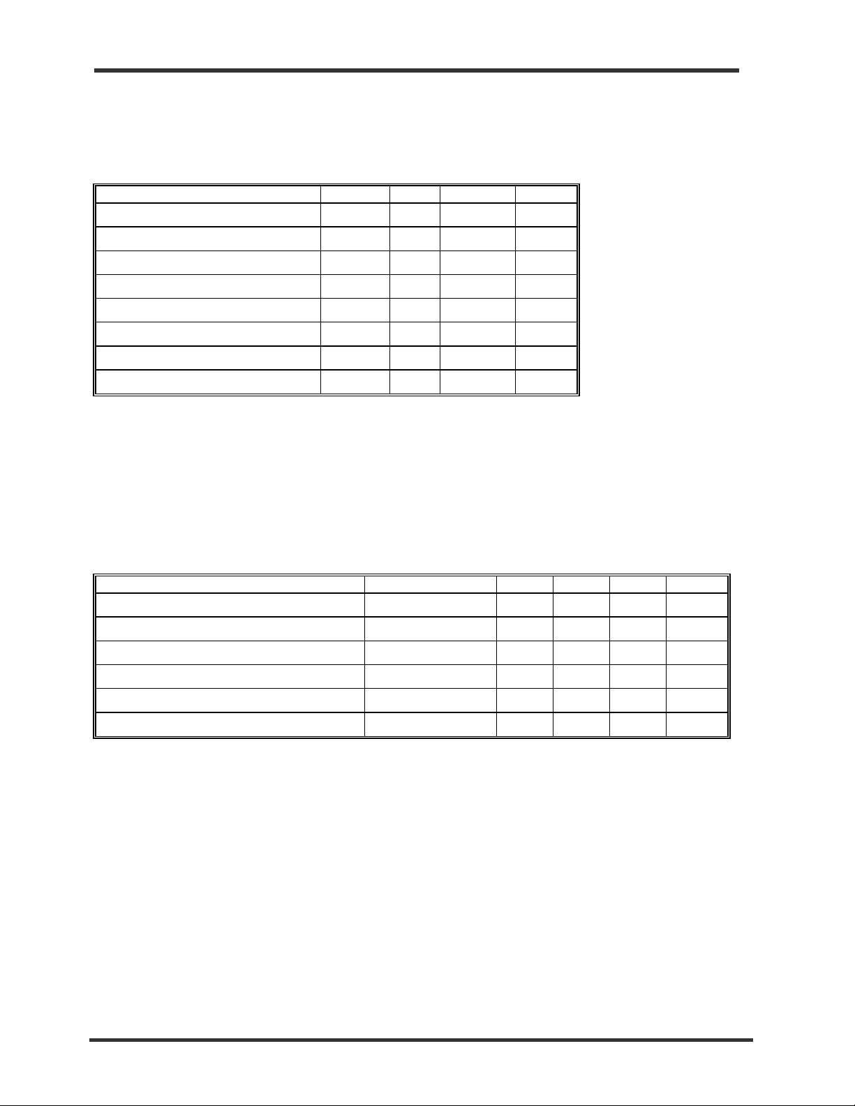
Table 4. Operating Conditions
Parameter Min Typ Max Units
Ambient Operating Temperature 0 70 °C
Operating Voltage, VDD 3 3.6 V
Input High Voltage, VIH, X1 pin only 2.5 1.65 V
Input Low Voltage, VIL, X1 pin only 1.65 0.5 V
Input High Voltage, VIH, OE pin 2 V
Input Low Voltage, VIL, OE pin 0.8 V
Input High Voltage, VIH, trinary inputs VDD-0.5 V
Input Low Voltage, VIL, trinary inputs 0.5 V
DC Characteristics
Table 5. DC Characteristics
VDD = 3V to 3.6V
Parameter Condition Min Typ Max Units
Output High Voltage, VOH I
Output Low Voltage, VOL I
Operating Supply Current, I
Short Circuit Current CLK output ±100 mA
Input Capacitance S0, S1, OE, X1, X2 4 pF
Frequency synthesis error 0 ppm
(20 MHz Xtal) No Load, 100MHz 25 mA
DD
=-25mA 2.4 V
OH
=25mA 0.4 V
OL
2002-02-25 Page 3 MDST-0017-02
Vaishali Semiconductor 747 Camden Avenue, Suite C Campbell CA 95008 Ph. 408.377.6060 Fax 408.377.6063
www.vaishali.com
Page 4
VT98521
AC Characteristics
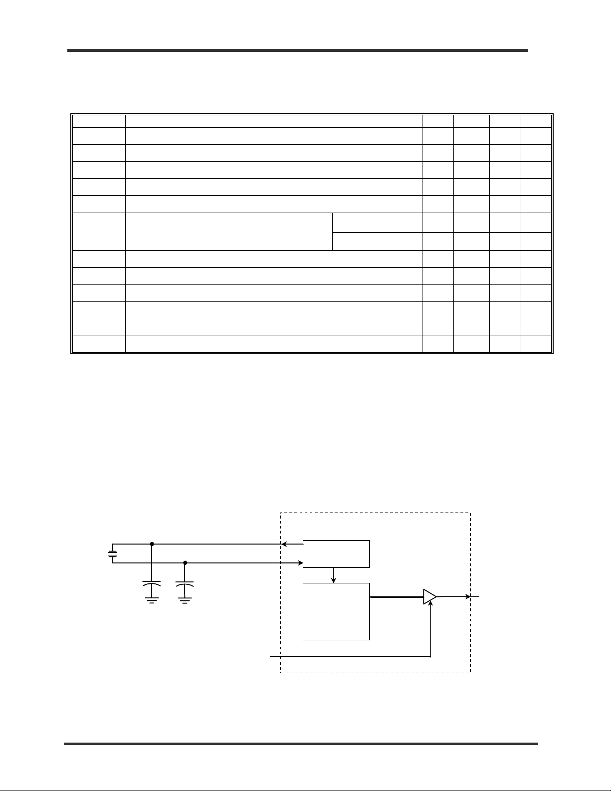
Table 6 AC Characteristics
VDD = 3V to 3.6V over the operating temperature range
Symbol Parameter Condition Min Typ Max Units
f
Input Crystal Frequency 5 27 MHz
osc
fin Input clock frequency 5 50 MHz
f
Output Frequency, 24 220 MHz
out
tr Output Clock Rise Time 0.8 to 2.0V 1 ns
tf Output Clock Fall Time 2.0 to 0.8V 1 ns
up to 160 MHz 45 49 to 51 55 % tod Output Clock Duty Cycle 1.5 V
160 MHz to 220 MHz 40 60 %
PLL Bandwidth 10 kHz
T
PZH, TPZL
T
PHZ, TPLZ
t
jit
t
jit
Output Enable Time, OE high to output on 50 ns
Output Disable time, OE low to Tri-state 50 ns
(abs) Absolute Clock period Jitter Deviation from mean
f
= 160 MHz
out
(sigma) One Sigma Clock Period Jitter f
= 160 MHz 25 ps
out
70 ps
Note1: External Crystal Connection.
The external crystal should be connected in as close physical proximity to the VT98521 as possible. The crystal should be a
fundamental mode, parallel resonant. Do not use third overtone. External load capacitors should be fitted in accordance with the
crystal manufacturer’s specifications.
Note2: Decoupling and termination.
Decoupling capacitors of 0.01 µF and 0.1 µF should be connected between VDD and Ground. Capacitors should be mounted as
close to the chip as possible. A 33Ω termination resistor may be connected in series with the clock output in order to minimize ringing
and reflections.
Figure 3. External Crystal Connection Block Diagram
Crystal
CX2
CX1
33pF
C
External Crystal
External Crystal
Load Capacitors
Load Capacitors
2002-02-25 Page 4 MDST-0017-02
Vaishali Semiconductor 747 Camden Avenue, Suite C Campbell CA 95008 Ph. 408.377.6060 Fax 408.377.6063
X2
X2
XTAL OSC
XTAL OSC
X1
X1
CLK3
X1
PLL
PLL
CLOCK
CLK
106.25MHz
GEN.
OE
OE
www.vaishali.com
Page 5
VT98521
A
A
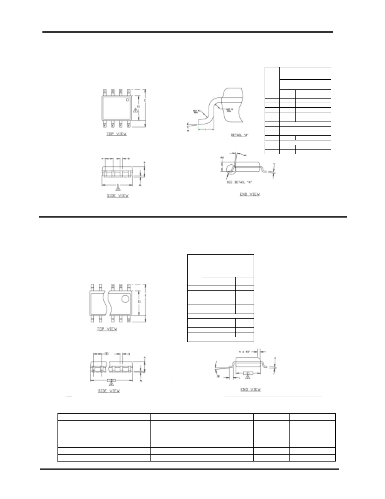
Package Dimensions.
MSOP
VARIATIONS
A1 0 - 0.15
A2 0.75 0.85 0.95
E1 3.00 BSC
oc 0° - 8°
OC1 5° - 15°
(ALL ARE IN MM)
AA
SYMBOLS
MIN NOM MAX
A - - 1.1
b 0.22 - 0.38
c 0.08 - 0.23
D 3.00 BSC
E 4.90 BSC
L 0.4 0.6 0.8
e 0.65
ll dimensions are in millimeters
SOIC
VARIATIONS
(ALL ARE IN MM)
AA
SYMBOLS
MIN NOM MAX
A 1.35 1.55 1.75
A1 .011 - 0.25
B 0.33 0.42 0.51
C 0.19 0.22 0.25
D 4.80 4.90 5.00
E1 3.80 3.90 4.00
e 1.27 BSC
E 5.80 6.00 6.20
h 0.25 0.38 0.50
oc 0° 5° 8°
L 0.40 - 1.27
N 8
ll dimensions are in millimeters
Ordering Information
Part Number Marking Shipping/Packaging No. of Pins Package Temperature
VT98521S1 VT98521S1 Tubes 8 SOIC 0oC to +70oC
VT98521S1X VT98521S1 Tape & Reel 8 SOIC 0oC to +70oC
VT98521M VT98521M Tubes 8 MSOP 0oC to +70oC
VT98521MX VT98521M Tape & Reel 8 MSOP 0oC to +70oC
VT98521/D Dice in waffle-packs 0oC to +70oC
VT98521/DW Dice in wafer form 0oC to +70oC
2002-02-25 Page 5 MDST-0017-02
Vaishali Semiconductor 747 Camden Avenue, Suite C Campbell CA 95008 Ph. 408.377.6060 Fax 408.377.6063
www.vaishali.com
 Loading...