

Page 1
.
Photoconductive Cells and
Photoconductive Cells and
Analog Optoisolators (V
Analog Optoisolators (V
actrols®)
actrols®)
Sensors
Telecom
Digital Imaging
Specialty Lighting
Lighting Imaging Telecom Sensors
Detectors and Sensors
Optoelectronics
Page 2

Optoswitches, optical hybrids, custom assemblies, photodiodes, phototransistors, IR
emitters, and photoconductive cells for industrial, commercial, and consumer electronics applications.
PerkinElmer Optoelectronics has the distinction of being one of the foremost manufacturers in
optoelectronics. Founded in 1947, PerkinElmer offers its customers over 35 years experience
in the development and application of optoelectronic devices. The product line is one of the
broadest in the industry, including a variety of standard catalog products as well as custom
design and manufacturing capabilities. Approximately 75% of the products shipped are custom designed and tested to serve the needs of specific OEM applications.
Three basic objectives guide PerkinElmer’s activities - Service, Quality, and Technology.
Our outstanding engineering staff, coupled with the implementation of modern material control
and manufacturing techniques, plus our commitment to quality, has gained PerkinElmer “certified” status with many major customers. Products are often shipped directly to manufacturing
lines without need for incoming QC at the customer’s facility. PerkinElmer’s products are vertically integrated, from the growing of LED crystals, silicon die fabrication, package design, reliability qualification, to assembly. Vertical integration is your assurance of consistent quality.
Recognizing the need for low-cost manufacturing to serve world markets, PerkinElmer
expanded its manufacturing/assembly operations into the Far East more than 20 years ago.
The combination of strong technology in processing at the St. Louis headquarters and lowcost assembly operations in the Far East has allowed PerkinElmer to effectively serve all
markets, worldwide. PerkinElmer provides optical sensors, IR emitters and subassemblies for
such diverse applications as street light controls, cameras, smoke alarms, business
machines, automotive sensors, and medical equipment.
For pricing, delivery, data sheets, samples, or technical support please contact your
PerkinElmer Sales Office or direct your questions directly to the factory.
PerkinElmer Optoelectronics
10900 Page Avenue
St. Louis, Missouri 63132 USA
Tel: (314) 423-4900 Fax: (314) 423-3956
Copyright 2001 by
PerkinElmer Optoelectronics
All rights reserved
www.perkinelmer.com/opto
..
Page 3

i
Table of Contents
Photoconductive Cells . . . . . . . . . . . . . . . . . . . . . . . . . . . . . . . . . . . . . . . . . . . . . . . . . . . . . . . . . . . . . . . . . . . . . . . . . . 1
What is a Photoconduc tive Cell? . . . . . . . . . . . . . . . . . . . . . . . . . . . . . . . . . . . . . . . . . . . . . . . . . . . . . . . . . . . . . . . . 2
Photoconduct i ve Cell Typical Applications . . . . . . . . . . . . . . . . . . . . . . . . . . . . . . . . . . . . . . . . . . . . . . . . . . . . . . . . . 3
Why Use Photocells? . . . . . . . . . . . . . . . . . . . . . . . . . . . . . . . . . . . . . . . . . . . . . . . . . . . . . . . . . . . . . . . . . . . . . 3
Applications . . . . . . . . . . . . . . . . . . . . . . . . . . . . . . . . . . . . . . . . . . . . . . . . . . . . . . . . . . . . . . . . . . . . . . . . . . . . . 3
Photoconduct i ve Cell Typical Application Circuit s . . . . . . . . . . . . . . . . . . . . . . . . . . . . . . . . . . . . . . . . . . . . . . . . . . . 4
Selecting a Photocell . . . . . . . . . . . . . . . . . . . . . . . . . . . . . . . . . . . . . . . . . . . . . . . . . . . . . . . . . . . . . . . . . . . . . . . . . 5
Photoconduct i ve Cell Typical Characteristic Curves @ 25°C Type Ø Material . . . . . . . . . . . . . . . . . . . . . . . . . . . . . 9
Type Ø Material . . . . . . . . . . . . . . . . . . . . . . . . . . . . . . . . . . . . . . . . . . . . . . . . . . . . . . . . . . . . . . . . . . . . . . . . . . 9
Photoconduct i ve Cell Typical Characteristic Curves @ 25°C Type 3 Material . . . . . . . . . . . . . . . . . . . . . . . . . . . . 11
Type 3 Material . . . . . . . . . . . . . . . . . . . . . . . . . . . . . . . . . . . . . . . . . . . . . . . . . . . . . . . . . . . . . . . . . . . . . . . . . 11
Photoconduct i ve Cell Tes ting and General Notes . . . . . . . . . . . . . . . . . . . . . . . . . . . . . . . . . . . . . . . . . . . . . . . . . . 13
Production Testing of Photocells - PerkinElmer’s New Approach . . . . . . . . . . . . . . . . . . . . . . . . . . . . . . . . . . . . . . 13
Device Specifications . . . . . . . . . . . . . . . . . . . . . . . . . . . . . . . . . . . . . . . . . . . . . . . . . . . . . . . . . . . . . . . . . . . . . . . . 14
Plastic Coated
VT900 Series . . . . . . . . . . . . . . . . . . . . . . . . . . . . . . . . . . . . . . . . . . . . . . . . . . . . . . . . . . . . . . . . . . . . . . . . . . . 14
VT800 Series . . . . . . . . . . . . . . . . . . . . . . . . . . . . . . . . . . . . . . . . . . . . . . . . . . . . . . . . . . . . . . . . . . . . . . . . . . . 15
VT800CT Series . . . . . . . . . . . . . . . . . . . . . . . . . . . . . . . . . . . . . . . . . . . . . . . . . . . . . . . . . . . . . . . . . . . . . . . . 16
VT400 Series . . . . . . . . . . . . . . . . . . . . . . . . . . . . . . . . . . . . . . . . . . . . . . . . . . . . . . . . . . . . . . . . . . . . . . . . . . . 17
Glass/Metal (Hermetic) Case
VT200 Series . . . . . . . . . . . . . . . . . . . . . . . . . . . . . . . . . . . . . . . . . . . . . . . . . . . . . . . . . . . . . . . . . . . . . . . . . . . 18
VT300 Series . . . . . . . . . . . . . . . . . . . . . . . . . . . . . . . . . . . . . . . . . . . . . . . . . . . . . . . . . . . . . . . . . . . . . . . . . . . 19
VT300CT Series . . . . . . . . . . . . . . . . . . . . . . . . . . . . . . . . . . . . . . . . . . . . . . . . . . . . . . . . . . . . . . . . . . . . . . . . 20
VT500 Series . . . . . . . . . . . . . . . . . . . . . . . . . . . . . . . . . . . . . . . . . . . . . . . . . . . . . . . . . . . . . . . . . . . . . . . . . . . 21
Applicatio n Not es—P hotoconductive Cells . . . . . . . . . . . . . . . . . . . . . . . . . . . . . . . . . . . . . . . . . . . . . . . . . . . . . . . 22
APPLICATION NOTE #1 Light - Some Physical Basics . . . . . . . . . . . . . . . . . . . . . . . . . . . . . . . . . . . . . . . . . . 22
APPLICATION NOTE #2 Light Resistance Measurement Techniques . . . . . . . . . . . . . . . . . . . . . . . . . . . . . . . 23
APPLICATION NOTE #3 Spectral Output of Common Light Sources . . . . . . . . . . . . . . . . . . . . . . . . . . . . . . . 23
APPLICATION NOTE #4 Spe ct ralMatching of LEDsand Photocondu ct ive Typ es . . . . . . . . . . . . . . . . . . . . . 24
APPLICATION NOTE #5 Assembly Precautions . . . . . . . . . . . . . . . . . . . . . . . . . . . . . . . . . . . . . . . . . . . . . . . 25
APPLICATION NOTE #6 A Low Cost Light Source for Measuring Photocells . . . . . . . . . . . . . . . . . . . . . . . . . 25
APPLICATION NOTE #7 How to Specify a Low Cost Photocell . . . . . . . . . . . . . . . . . . . . . . . . . . . . . . . . . . . . 26
Page 4

ii
Table of Conte nts (Continued)
Analog Optical Isolators VACTROLS® . . . . . . . . . . . . . . . . . . . . . . . . . . . . . . . . . . . . . . . . . . . . . . . . . . . . . . . . . . . . 27
What Are Analog Optical Isolators? . . . . . . . . . . . . . . . . . . . . . . . . . . . . . . . . . . . . . . . . . . . . . . . . . . . . . . . . . . . . . 28
Typical Applications of Analog Optical Isolators . . . . . . . . . . . . . . . . . . . . . . . . . . . . . . . . . . . . . . . . . . . . . . . . . . . . 32
Characteristics of Analog Optical Isolators . . . . . . . . . . . . . . . . . . . . . . . . . . . . . . . . . . . . . . . . . . . . . . . . . . . . . . . . 34
Transfer Characteristics . . . . . . . . . . . . . . . . . . . . . . . . . . . . . . . . . . . . . . . . . . . . . . . . . . . . . . . . . . . . . . . . . . . 34
Response Time . . . . . . . . . . . . . . . . . . . . . . . . . . . . . . . . . . . . . . . . . . . . . . . . . . . . . . . . . . . . . . . . . . . . . . . . . 34
Noise . . . . . . . . . . . . . . . . . . . . . . . . . . . . . . . . . . . . . . . . . . . . . . . . . . . . . . . . . . . . . . . . . . . . . . . . . . . . . . . . . 34
Distortion . . . . . . . . . . . . . . . . . . . . . . . . . . . . . . . . . . . . . . . . . . . . . . . . . . . . . . . . . . . . . . . . . . . . . . . . . . . . . . 35
Voltage Rating . . . . . . . . . . . . . . . . . . . . . . . . . . . . . . . . . . . . . . . . . . . . . . . . . . . . . . . . . . . . . . . . . . . . . . . . . . 37
Power Rating . . . . . . . . . . . . . . . . . . . . . . . . . . . . . . . . . . . . . . . . . . . . . . . . . . . . . . . . . . . . . . . . . . . . . . . . . . . 37
Life and Aging . . . . . . . . . . . . . . . . . . . . . . . . . . . . . . . . . . . . . . . . . . . . . . . . . . . . . . . . . . . . . . . . . . . . . . . . . . 37
Storage Characteristics . . . . . . . . . . . . . . . . . . . . . . . . . . . . . . . . . . . . . . . . . . . . . . . . . . . . . . . . . . . . . . . . . . . 38
Temperature Range . . . . . . . . . . . . . . . . . . . . . . . . . . . . . . . . . . . . . . . . . . . . . . . . . . . . . . . . . . . . . . . . . . . . . . 38
Capacitance . . . . . . . . . . . . . . . . . . . . . . . . . . . . . . . . . . . . . . . . . . . . . . . . . . . . . . . . . . . . . . . . . . . . . . . . . . . . 39
Summary . . . . . . . . . . . . . . . . . . . . . . . . . . . . . . . . . . . . . . . . . . . . . . . . . . . . . . . . . . . . . . . . . . . . . . . . . . . . . . 39
Typical Transfer C haracteristics (Resis tan ce vs. Input Current) For Standar d Vactrols . . . . . . . . . . . . . . . . . . 40
Analog Optoisolator Comparison Chart . . . . . . . . . . . . . . . . . . . . . . . . . . . . . . . . . . . . . . . . . . . . . . . . . . . . . . . 41
Device Specifications
VTL5C1, 5C2 . . . . . . . . . . . . . . . . . . . . . . . . . . . . . . . . . . . . . . . . . . . . . . . . . . . . . . . . . . . . . . . . . . . . . . . . . . . 43
VTL5C3, 5C4 . . . . . . . . . . . . . . . . . . . . . . . . . . . . . . . . . . . . . . . . . . . . . . . . . . . . . . . . . . . . . . . . . . . . . . . . . . . 45
VTL5C2/2, 5C3/2 . . . . . . . . . . . . . . . . . . . . . . . . . . . . . . . . . . . . . . . . . . . . . . . . . . . . . . . . . . . . . . . . . . . . . . . . 47
VTL5C4/2 . . . . . . . . . . . . . . . . . . . . . . . . . . . . . . . . . . . . . . . . . . . . . . . . . . . . . . . . . . . . . . . . . . . . . . . . . . . . . . 49
VTL5C6, 5C7 . . . . . . . . . . . . . . . . . . . . . . . . . . . . . . . . . . . . . . . . . . . . . . . . . . . . . . . . . . . . . . . . . . . . . . . . . . . 50
VTL5C8 . . . . . . . . . . . . . . . . . . . . . . . . . . . . . . . . . . . . . . . . . . . . . . . . . . . . . . . . . . . . . . . . . . . . . . . . . . . . . . . 51
VTL5C9, 5C10 . . . . . . . . . . . . . . . . . . . . . . . . . . . . . . . . . . . . . . . . . . . . . . . . . . . . . . . . . . . . . . . . . . . . . . . . . . 55
Application Notes—Analog Optical Isolators . . . . . . . . . . . . . . . . . . . . . . . . . . . . . . . . . . . . . . . . . . . . . . . . . . . . . . 57
APPLICATION NOTE #1 Audio Applications . . . . . . . . . . . . . . . . . . . . . . . . . . . . . . . . . . . . . . . . . . . . . . . . . . . 57
APPLICATION NOTE #2 Handling and Soldering AOIs . . . . . . . . . . . . . . . . . . . . . . . . . . . . . . . . . . . . . . . . . . 67
APPLICATION NOTE #3 Rec om m ended Cleaning Agents . . . . . . . . . . . . . . . . . . . . . . . . . . . . . . . . . . . . . . . . 68
Page 5
iii
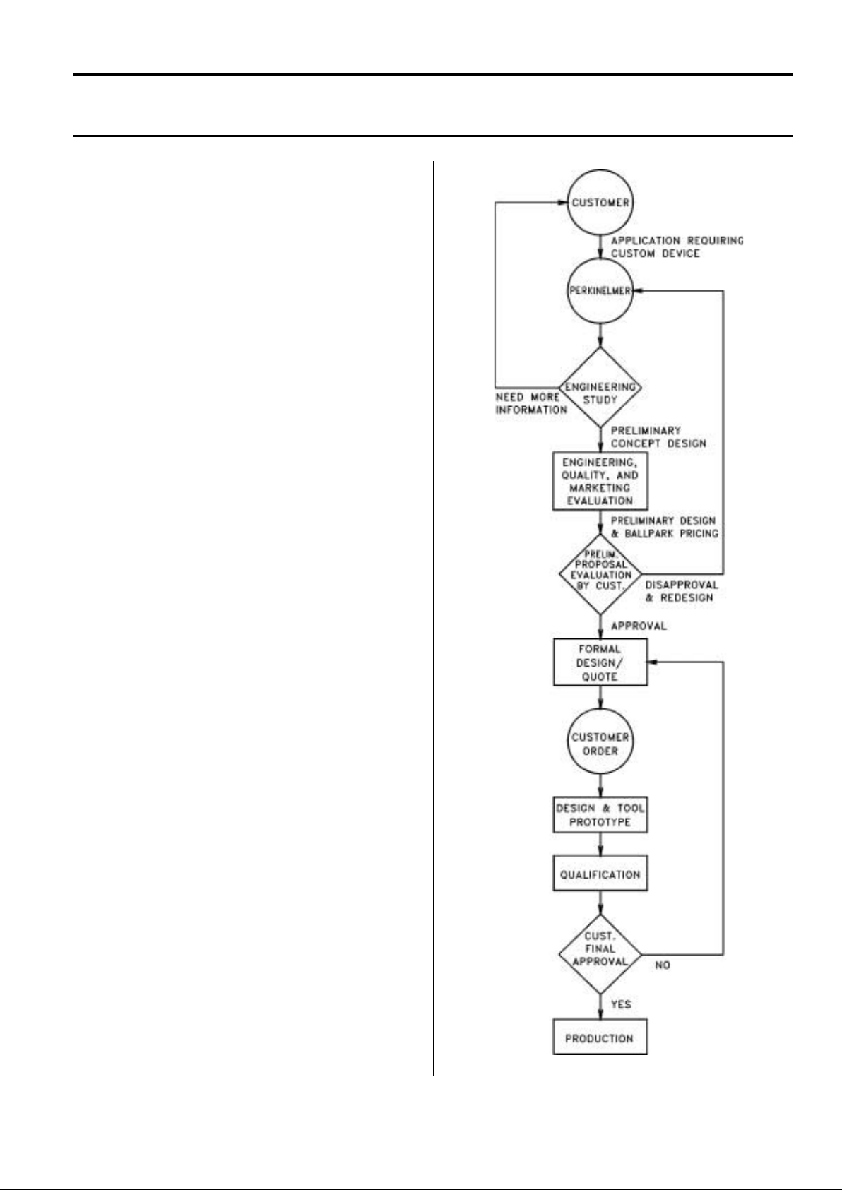
Custom and Semi-Custom Devices
Upon request, and where sufficient quantities are involved,
PerkinElmer Optoelectronics will test standard parts to your
unique set of specifications. The advantage of testing parts
under ac tual op erating co nditi ons is pred ictable performa nce in
the application.
PerkinElmer offers a broad line of standard photodiodes in a
wide var iety o f packa ges and sensit ivities. Nevert heless, some
application s demand a totally cu stom device. Reco gnizing this
real need, PerkinElmer’s engineering, research, and sales
departments are geared for working with the customer from
initial conc ep t throu gh des ign, pr otot ype , and v olum e pr od uct ion.
A custom design usually required the commitment of valuable
resourc es. Perki nElmer revi ews requ ests for cu stom devi ces on
a case by case basis and reserves the right to decide if the
business potential warrant s the under taking of such a project.
The customer may be asked to share in the expense of
development.
PerkinElmer has designed and fabricated custom products for
many companies. PerkinElmer’s staff can work closely with the
custom er and protect propriet ary infor mation. A cu stom design
usually required the commitment of valuable resources.
PerkinEl mer reviews requ ests for cu stom devices on a case by
case basis and reserves the right to decide if the business
potential warrants the undertaking of such a project. The
custom er ma y be asked to share i n the expense of deve lo pment.
PerkinElmer has designed and fabricated custom products for
many companies. PerkinElmer’s staff can work closely with the
custom er and protect propriet ary informat ion.
Your inquiries to PerkinElmer should include electrical,
environ mental, an d mechanica l require ments. Also, infor mation
on anticipated volumes, price objectives, and lead times is
helpful sinc e these often det ermine the choices of desi gn and
tooling.
Page 6
1
Photoconductive Cells
Page 7
2
What is a Photoconductive Cell?
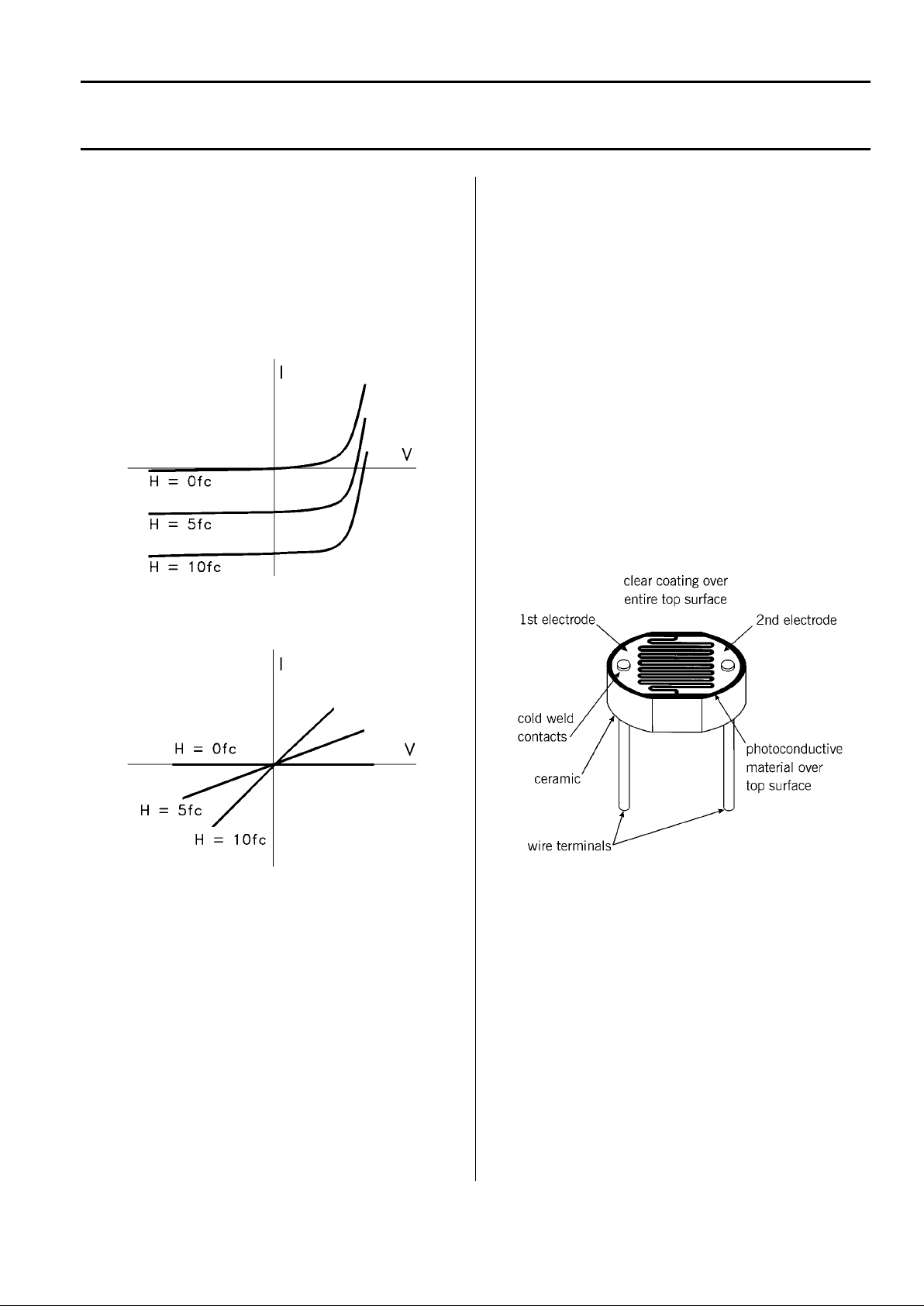
Semiconductor light detectors can be divided into two major
categories: junction and bulk effect devices. Junction devices, when
operated in the photoconductive mode, utilize the reverse
characteristic of a PN junction. Under reverse bias, the PN junction
acts as a light controlled current source. Output is proportional to
incident illumination and is relatively independent of implied voltage as
shown in Figure 1. Silicon photodiodes are examples of this type
detector.
Figure 1
Junc tion Photoconductor (Photodiode)
Figure 2
Bulk Effect Photoconduc tor (Photocell)
In contrast, bulk effect photoconductors have no junction. As shown in
Figure 2, the bulk resistivity decreases with increasing illumination,
allowing more photocurrent to flow. This resistive characteristic gives
bulk effect photoconductors a unique quality: signal current from the
detector can be varied over a wide range by adjusting the applied
voltage. To clearly make this distinction, PerkinElmer Optoelectronics
refers to it’s bulk effect photoconductors as photoconductive cells or
simply photocells.
Photocells are thin film devices made by depositing a layer of a
photoconductive material on a ceramic substrate. Metal contacts are
evaporated over the surface of the photoconductor and external
electrical connection is made to these contacts. These thin films of
photoconductive material have a high sheet resistance. Therefore, the
space between the two contacts is made narrow and interdigitated for
low cell resistance at moderate light levels. This construction is shown
in Figure 3.
Figure 3
Typical Construction of a Plastic Coated Photocell
Page 8

3
Photoconductive Cell Typical Applications
Why Us e Photocells?
Photocells can provide a very economic and technically superior solution for many applications where the presence or absence of light is sensed
(digital operation) or where the intensity of light needs to be measured (analog operation). Their general characteristics and features can be
summarized as follows:
• Lowes t cost available and near-IR photo det ector
• Available in low cost plastic encapsulated packages as well as hermetic packages (TO-46, TO-5, TO-8)
• Responsive to both very low light levels (m oonlight) and to very high ligh t levels (direct sunlight)
• Wide dynamic range: resistance change s of several ord er s of magnitude between "light" and "no light"
• Low noise distortion
• Maximum op er ating voltag es of 50 t o 400 volts are suitable for oper at ion on 120/240 VAC
• Available in center tap dual cell configurations as well as speciall y selected resistance ranges for special appl ications
• Easy to use in DC or AC circuits - they are a light v ariable resistor and hence sym m et rica l with respect to AC wa veforms
• Usable with almost any visible or near infrared light source such as LEDS; neon; fluorescent, incandescent bulbs, lasers; flame sou rces;
sunlight; etc
• Available in a wide range of resistance values
Applications
Photoconductive cells are used in many different types of circuits and applications.
Analog Applications
• Camera Exposure Control
• Auto Sl ide Focus - dual cell
• Photocopy Machines - density of toner
• Colorimetric Test Equipment
• Densitometer
• Electronic Scales - dual cell
• Autom at ic G ain Control - modulated light source
• Autom ated Rear View Mirror
Digital Applications
• Autom atic Headlight Dimmer
• Night Light Control
• Oil Burner Flame Out
• Street Light Control
• Absence / Presence ( beam breaker)
• P osition Sensor
Page 9
4
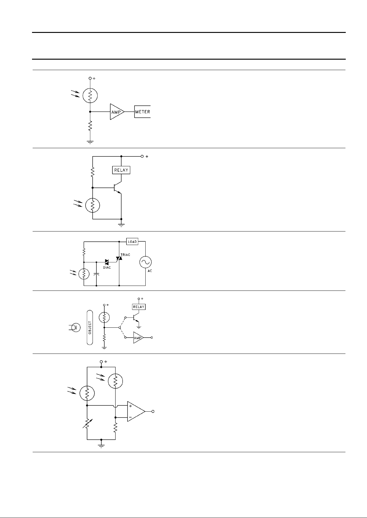
Photoconductive Cell Typ ical Application Circuits
Ambient Light Measurement
Camera Exposure Meter (VT900)
Brig htness Co ntrol (V T9 00)
DC Relay
Rear View Mirror Control (VT200)
Head Light Dimmer (VT300 or VT800)
AC Rela y
Night Light Control (VT800 or VT 900)
Street Light Control (VT400)
Flame Detector (VT400 or 500)
Object Sensing / Measurement
Beam Breaking Applications (VT800)
Security Systems (VT800 or VT900)
Colo rim et ri c Test Equipment (VT20 0 or VT300)
Densitometer (V T200 or VT300)
Bridge Circuits
Auto Focus (VT300CT or VT800CT)
Elect r onic Scal es (VT300CT or VT800CT )
Photoelect ric Se rvo (VT300CT or VT 800CT)
Page 10
5
Selecting a Photocell
Specifying the best photoconductive cell for your application requires
an understanding of its principles of operation. This section reviews
some fundamentals of photocell technology to help you get the best
blend of par am eters for your application.
When selecting a photocell the design engineer must ask two basic
questions:
1. What kind of performance is required from the cel l?
2. What kind of environment must the cell work in?
Perfor mance Criteria
Sensitivity
The sensitivity of a photodetector is the relationship between the light
falling on the device and the resulting output signal. In the case of a
photocell, one is deali ng with the rela tionsh ip betw een the in cident light
and the corresponding resistance of the cell.
Defining the sensitivity required for a specific application can prove to
be one of the more difficult aspects in specifying a photoconductor. In
order to specify the sensitivity one must, to some degree, characterize
the light source in terms of its intensity and its spectral content.
Within this handbook you will find curves of resistance versus light
intensity or illumination for many of PerkinElm er ’s stock photocells. T he
illumination is expressed in units of fc (foot candles) and lux. The light
source is an incandescent lamp. This lamp is special only in that the
spectral composition of the light it generates matches that of a black
body at a color temperature of 2850 K. This type of light source is an
industry agreed to standard.
Over the years PerkinElmer has developed different “types” of
photoconductive materials through modification s ma de to the chemical
composition of the detector. For a given type of photoconductor
material, at a given level of illumination, the photoconductive film will;
have a certain sheet resistivity. The resistance of the photocell at this
light level is determined by t he electrode geometry.
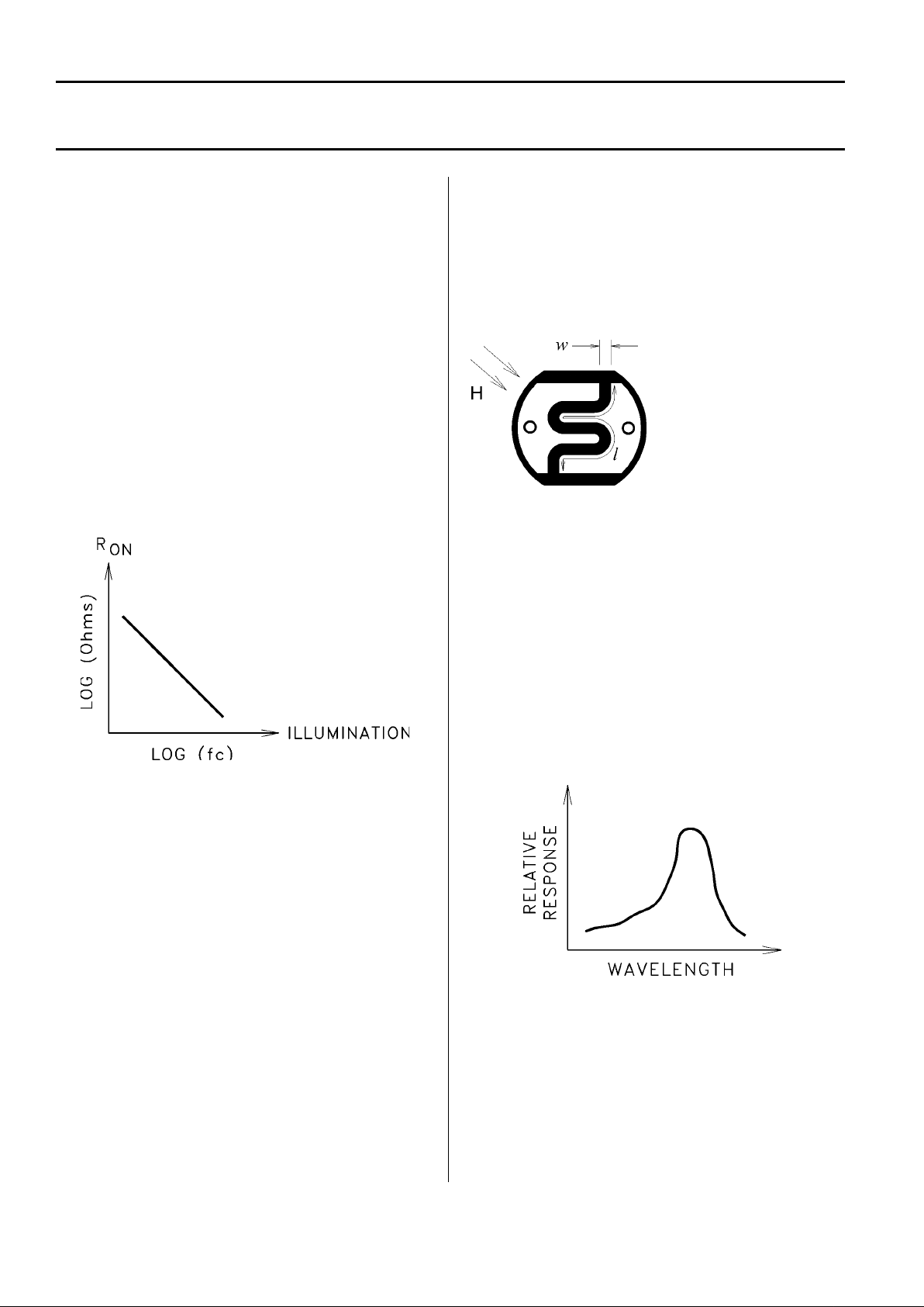
R
H
=
ρH (w / l )
where:
R
H
= resistance of cell at light
level H
ρH = sheet resistivity of
photoconductive film at light level
H
w = width of electro de gap
l = length of electrode gap
Sheet sensitivity (
ρH) for
photocond uct ive films at 2 fc are in the r ange of 20 MΩ per square.
The ratio w / l can be varied over a wide range in order to achieve
design goals. Typical values for w / l run from 0.002 to 0.5, providing
flexibility for terminal resistance and maximum cell voltage.
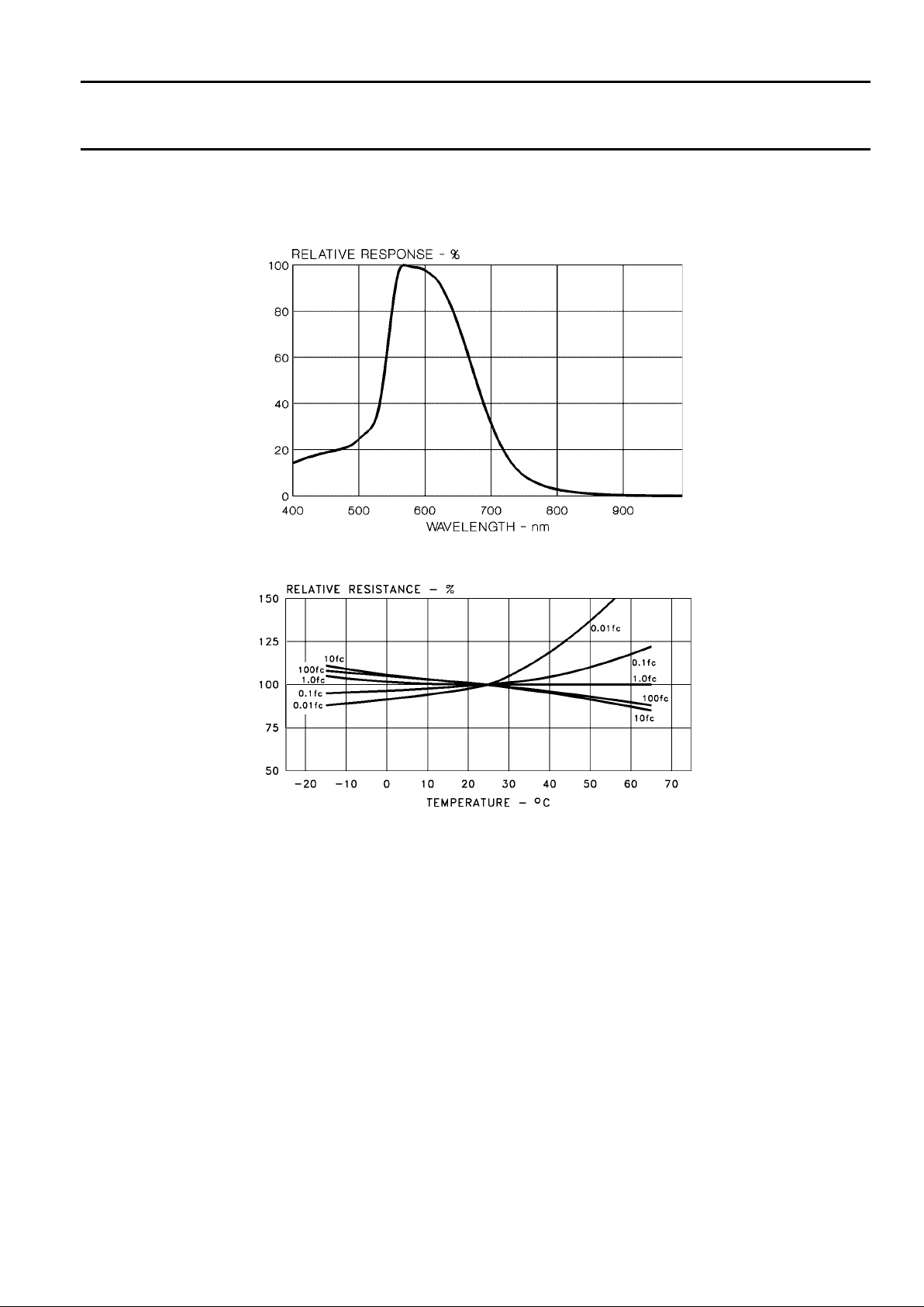
Spectral Response
Like the human eye, the relative sensitivity of a photoconductive cell is
dependent on the wavelength (color) of the incident light. Each
photoconductor material type has its own unique spectral response
curve or plot of the relative response of the photocell versus
wav elength of light.
The spectral response curves for PerkinElmer’s material types are
given in the handbook and should be considered in selecting a
photocell f or a particular application.
Page 11
6
Selecting a Photocell
Slope Characteristics
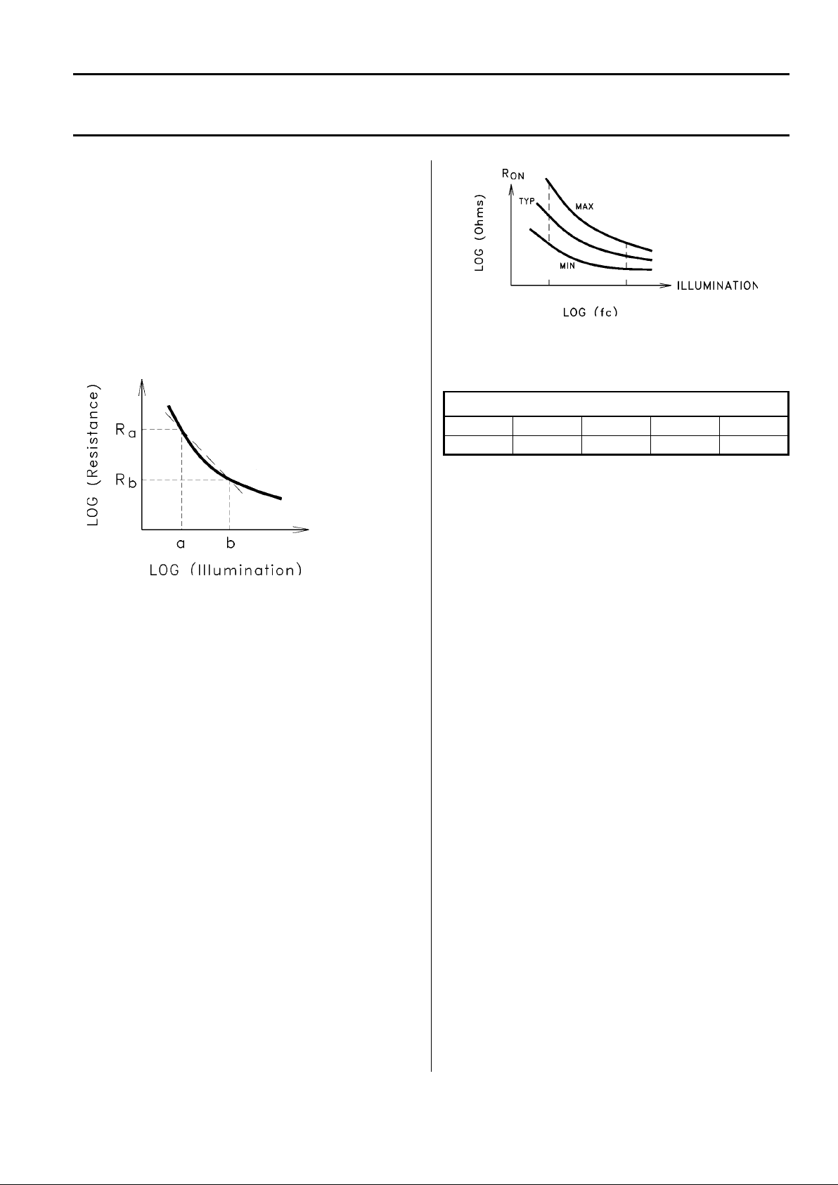
Plots of the resistance for the photocells listed in this catalog versus
light intensit y result in a series of curves with characteristic ally diff eren t
slopes. This is an important characteristic of photocells because in
many applications not only is the absolute value of resistance at a
given light level of concern but also the value of the resistance as the
light source is varied. One way t o specify this relationship is by the use
of parameter (gamma) which is defined as a straight line passing
through two specific points on the resistance curve. The two points
used by PerkinElmer to define
γ
are 10 lux (0.93 fc) and 100 lux (9.3
fc).
Applications for photocells are of one of two categories: digital or
analog. For the digital or ON-OFF types of applications such as flame
detectors, cells with steep slopes to their resistance versus light
intensity curves are appropriate. For analog or measurement types of
applications such as exposure controls for cameras, cells with shallow
slopes might be bet ter suited.
Resistance Tolerance
The sensitivity of a photocell is defined as its resistance at a specific
level of illumination. Since no two photocells are exactly alike,
sensitivity is stated as a typical resistance value plus an allowable
tolerance. Both the value of resistance and its tolerance are specified
for only one light level. For moderate excursions from this specified
light level the tolerance level remain more or less constant. However,
when th e light level the t oleran ce level r emain more or less c onst ant.
However, when the light level is decades larger or smaller than the
reference level the tolerance can differ considerably.
As the light level decreases, the spread in the tolerance level
increases. For increasing light levels the resistance tolerance will
tighten.
Likewise, for dual element photocells the matching factor, which is
defined as the ratio of the resistance of between elements, will
increase with decreasing light level.
Dark Resistance
As the name implies, the dark resistance is the resistance of the cell
under zero illumination lighting conditions. In some applications this
can be very important since the dark resistance defines what
maximum “leakage current” can be expected when a given voltage is
applied across the cell. Too high a leakage current could lead to false
triggering in some appl ications.
The dark resistance is often defined as the minimum resistance that
can be expected 5 seconds after the cell has been removed from a
light intensit y of 2 fc. Typical v alues f or dark resist ance tend to be in the
500k ohm to 20M ohm range.
T emperature Coefficient of Res ist ance.
Each type of photoconductive material has its own resistance versus
temperature characteristic. Additionally, the temperature coefficients of
photoconductors are also dependent on the light level the cells are
operating at.
From the curves of the various types of materials it is apparent that the
temperatu re coeff ic ient is an in ver se funstin of li ght le vel . Thus, in order
to minimize temperature problems it is desirable to have the cell
operatin g at t he highest light lev el possible.
Speed of Response
Speed of response is a measure of the speed at which a photocell
responds to a change from light-to-dark or from dark-to-light. The rise
time is defined as the time necessary for the light conductance of the
photocell to rea c h 1- 1/e (or about 63%) of its fina l value.
γ
Log Ra Log Rb–
Log a Lob b–
------------------------------------ -=
Log Ra Rb⁄()
Log b a⁄()
------------------------------=
Dual Element Photocell Typical Matching Ratios
0.01 fc 0.1 fc 1.0 fc 10 fc 100 fc
0.63 – 1.39 0.74 – 1.27 0.75 – 1.25 0.76 – 1.20 0.77 – 1.23
Page 12
7
Selecting a Photocell
The decay or fall time is defined as the time necessary for the light
conductance of the photocell to decay to 1/e (or about 73%) of its
illuminat ed state. At 1 fc of i llumination the response times are typically
in the range of 5 msec to 100 msec.
The speed of response depends on a number of factors including light
level, light history, and ambient temperature. All material types show
faster speed at higher light levels and slower speed at lower light
levels. Storage in the dark will cause slower response than if the cells
are kept in the light. The longer the photocells are kept in the dark the
more pronounced this effect will be. In addition, photocells tend to
respond slow er in colder temperatures .
Light History
All photoconductive cells exhibit a phenomenon known as hysteresis,
light memory, or light history effect. Simply stated, a photocell tends to
remember its most recent storage condition (light or dark) and its
instantaneous conductance is a function of its previous condition. The
magnitude of the light history effect depends upon the new light level,
and upon the time spent at each of these light levels. this effect is
reversible.
To understand the light history effect, it is often convenient to make an
analog y between the response of a photocell and that of a human eye.
Like the cell, the human eye’s sensitivity to light depends on what level
of light it was recently exposed to. Most people have had the
exper ienc e of comi ng in fr om the o utdoo rs on a b right summe r’s day
and being temporarily unable to see under normal room levels of
illumination. your eyes will adjust but a certain amount of time must
elapse first. how quickly one’s eyes adjust depends on how bright it
was outside and how long you remained outdoors.
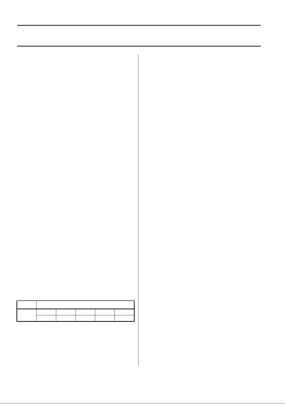
The following guide shows the general relationship between light
history and light resistance at various light levels. The values shown
were determined by dividing the resistance of a given cell, following
infinite light history (R
LH
), by the resistance of the same cell following
“infinite” dark history (RDH). For practical purposes, 24 hours in the
dark wil l ac hieve RDH or 24 hours at approximately 30 fc will achieve
RLH.
Typical V ariation of Resistance with Light History Expressed as a Ratio
R
LH
/
R
DH
at Various Test Illumination Levels.
This guide illustrates the fact that a photocell which has been stored for
a long time in the light will have a considerably higher light resistance
than if it was stored for a long time in the dark. Also, if a cell is stored
for a long period of time at a light level higher than the test level, it will
have a hi gher light resistance than if it was st or ed at a light level closer
to the test light level.
This effect can be minimized significantly by keeping the photocell
exposed to some constant low level of illumination (as opposed to
having it sit in the dark). This is the reason resistance specifications
are characteri zed after 16 hours light adep t.
Environmental/Circuitry Considerations
Packaging
In order to be protected from potentially hostile environments
photocells are encapsulated in either glass/metal (hermetic) package
or are covered with a clear plastic coating. While the hermetic
packages provide the greatest degree of protection, a plastic coating
represents a lower cost approach.
The disadvantage of plastic coatings is that they are not an absolute
barrier to eventual penetration by moisture. This can have an adverse
effect on cell life. However, plastic coated photocells have been used
successfully for many years in such h ost ile environments a s street light
controls.
T emperature Range
The chemistry of the photoconductive materials dictates an operating
and storage temperature range of –40°C to 75°C. It should be noted
that operation of the cell above 75°C does not usually lead to
catastrophic failure but the photoconductive surface may be damaged
leading to irr eversible changes in sensitivity.
The amount of resistance change is a function of time as well as
temperature. While changes of several hundred percent will occur in a
matter of a few minutes at 150°C, it will take years at 50°C to produce
that much change.
Power Dissipation
During operation, a cell must remain within its maximum internal
temperature rating of 75°C. Any applied power will raise the cell’s
temperature above ambient and must be considered.
Illumination
R
LH
/ RDH
Ratio
0.01 fc 0.1 fc 1.0 fc 10 fc 100 fc
1.55 1.35 1.20 1.10 1.10
Page 13
8
Selecting a Photocell
Many low voltage situations involve very little power, so that the
photocell can be small in size, where voltages and/or currents are
higher, the photocell must be physically larger so that the
semiconductor film can dissipate the he at.
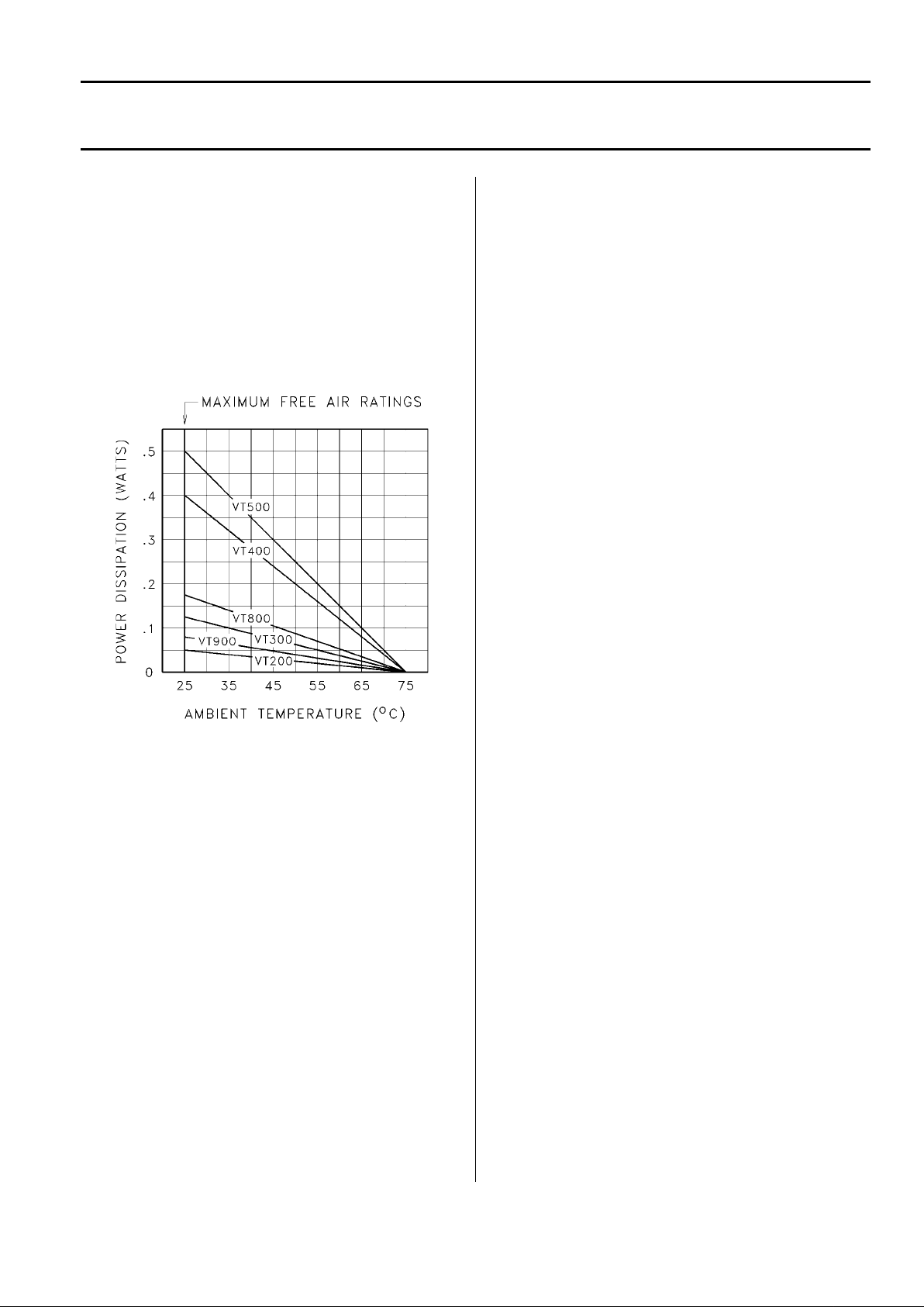
The following curve of power dissipation versus ambient temperature
describes the entire series of cells for operation in free air at room
ambient (25°C). Note that regardless the size, all photocells derate
linearly to zero at an ambient temperature of 75°C. The adequate heat
sinks can increase the dissipation by as much as four times the levels
shown in this graph.
Maximum Cell Voltage
At no time should the peak voltage of the cell exceed its maximum
voltage. the designer should determine the maximum operating or
peak voltage that the cell will experience in the circuit and choose an
appropriately rated cell. Ty pical volta ge r ates range from 100V to 300V.
What Type of Material is Best?
Each specific material type represents a trade off between several
characteristics. Selecting the best material is a process of determining
which characteristics are most important tin the application.
PerkinElmer’s standard photocells in this catalog are manufactured
using one of two different material types offered: type “Ø” or type “3”.
In general, material type “Ø” is used for applications such as
nightlights, automotive sensors. Material type “3” is primarily used in
camera, streetlight control, and flame detector applications.
Page 14
9
Photoconductive Cell Typical Characteristic Curves
@ 25°C Type Ø Material
Type Ø Material
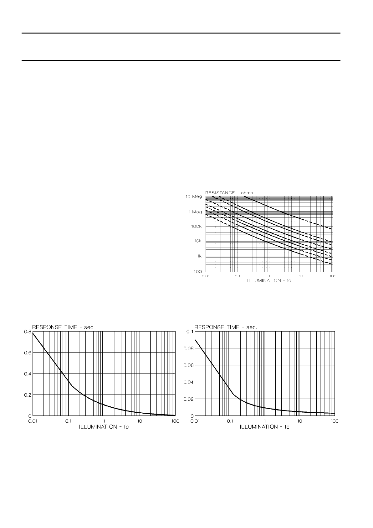
This is a general purpose material. Its characteristics include a good temperature coefficient and fast response time, especially at very
low light levels. Cells of this type have relatively low dark history. Ty pe Ø materia l is ofte n u sed in lig hti ng controls such as nightlights,
and security lighting.
The resistance for any standard catalog cell is controlled at only one light level. If the resistance at other light levels is a concern,
please contact the factory.
To obtain the typical re sistance versus illumination c haracteristic
for a specific part number:
1. Look up 2 footcandle resistance in table.
2. Insert res i stance given and dr aw a curve through t hat point
and par allel to the closest me m ber of the family of curves
shown for the appropriate type of photo-sensitive material.
Resistance vs. Illumina ti on
Response Time vs. Illumination
(Rise Time)
Response Time vs. Illumination
(Decay Time)
Page 15
10
Photoconductive Cell Typical Characteristic Curves
@ 25°C Type Ø Material
Relative Spectral Response
Relative Resistance vs. Temperature
Page 16
11
Photoconductive Cell Typical Characteristic Curves
@ 25°C Type 3 Material
Type 3 Material
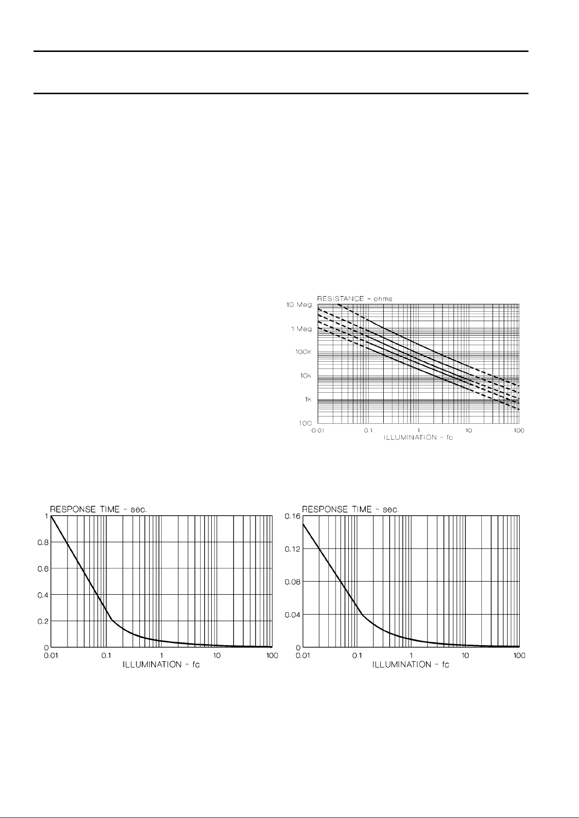
This i s a high speed materi al wit h a spectral response cl o sely approxima t ing the human eye. T hi s m at e rial i s well su i t e d fo r switching
from one light level t o an other and offers our best t em peratur e st abili t y an d r espon se ti m e. Th i s mater i al is often used i n ca meras and
indu st ri al controls.
The resistance for any standard catalog cell is controlled at only one light level. If the resistance at other light levels is a concern,
please contact the factory.
To obtain the typical re sistance versus illumination c haracteristic
for a specific part number:
1. Look up 2 footcandle resistance in table.
2. Insert res i stance given and dr aw a curve through t hat point
and par allel to the closest me m ber of the family of curves
shown for the appropriate type of photo-sensitive material.
Resistance vs. Illumina ti on
Response Time vs. Illumination
(Rise Time)
Response Time vs. Illumination
(Decay Time)
Page 17
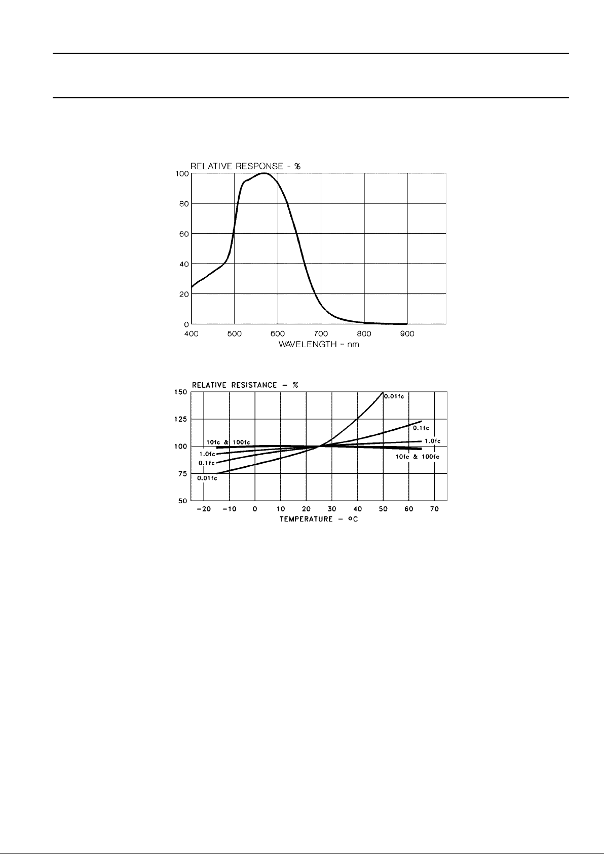
12
Photoconductive Cell Typical Characteristic Curves
@ 25°C Type 3 Material
Relative Spectral Response
Relative Resistance vs. Temperature
Page 18
13
Photoconductive Cell Testing and General Notes
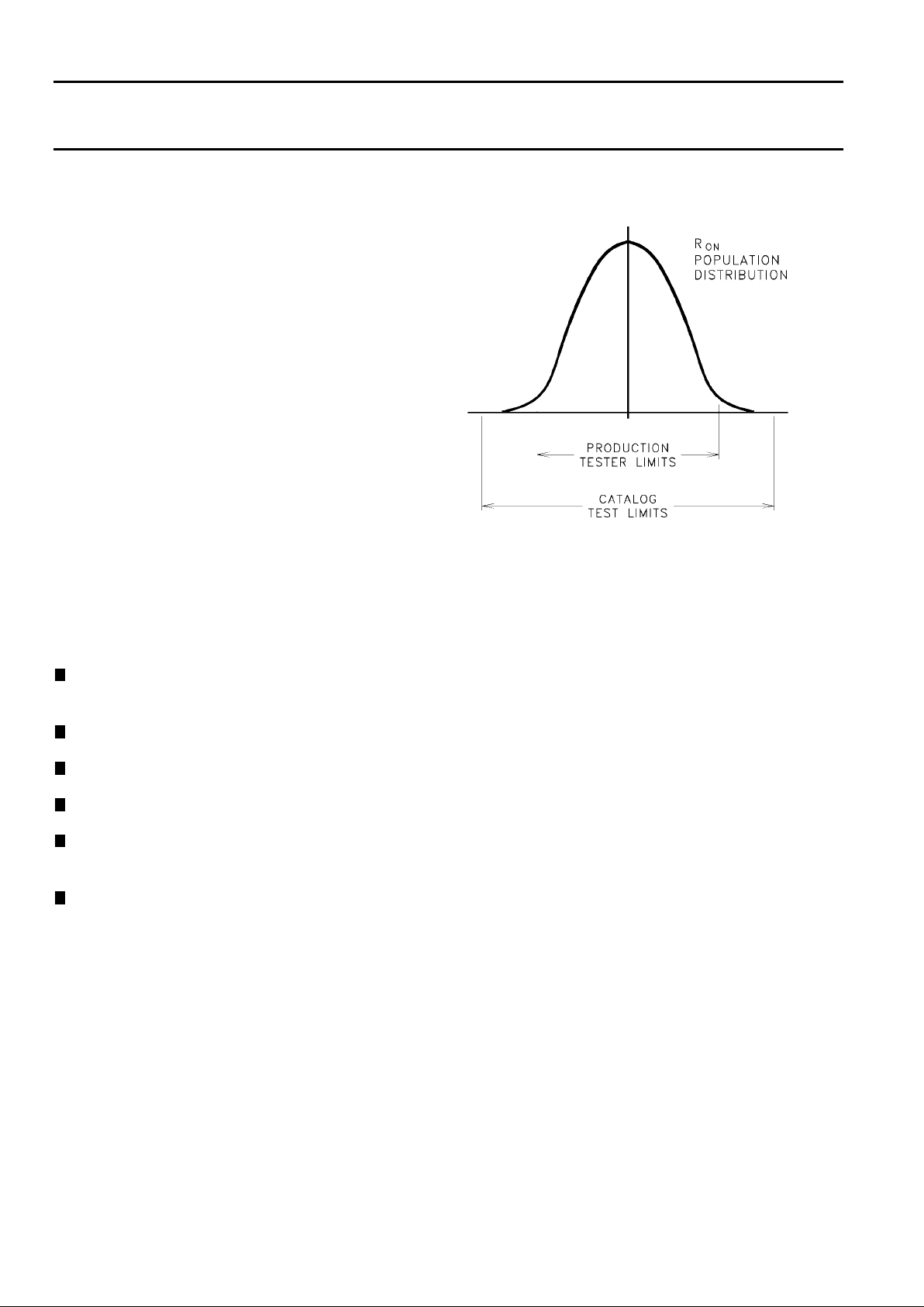
Production Testing of Photocells - PerkinElmer’s New Approach
Historically within this industry, vendors have set their
production testers to the limits specified on the
customer’s print. Measurement errors due to ambient
temperature, calibration of light source, light history
effect, plus any t ester errors have alw ays guaranteed that
a certain percentage of the cells shipped are out of
specification.
This practice is incompatible with the realities of today’s
marketp lac e, wh er e qual i ty level s are b ein g mea su red in
parts per million.
With this new catalog, PerkinElmer is taking the
opportunity to correct this situation. for parts in this
catalog, PerkinElmer has pulled in the test limits on our
production testers to compensate for measurement
errors.
General Notes
(Refer to the following data specification pages.)
Photocells a r e suppl i ed cat egorized into grou ps by resistance. All gr ou ps must be pur chased togethe r and Perk i nE l m er main t a i ns
the righ t to determine t he product m i x among the se groups.
Dimen si o n control l e d at ba se of package.
Photocells are tested at either 1 fc or 10 lux. 2 fc typical values shown in the tables are for reference only.
Cells are l ight adapted at 30 - 50 fc.
The photocell “grid” pattern ca n vary fr om that shown. Perki n El m er reserves t h e rig ht t o change mix gri d pa t tern s on any standard
product.
The re sis ta nce for any s tan dard ce ll is co ntr oll ed at onl y o ne l ight l evel. If the res ist ance at o th er ligh t levels is a co ncer n, p lea se
contact the factory .
1
2
3
4
5
6
Page 19
14
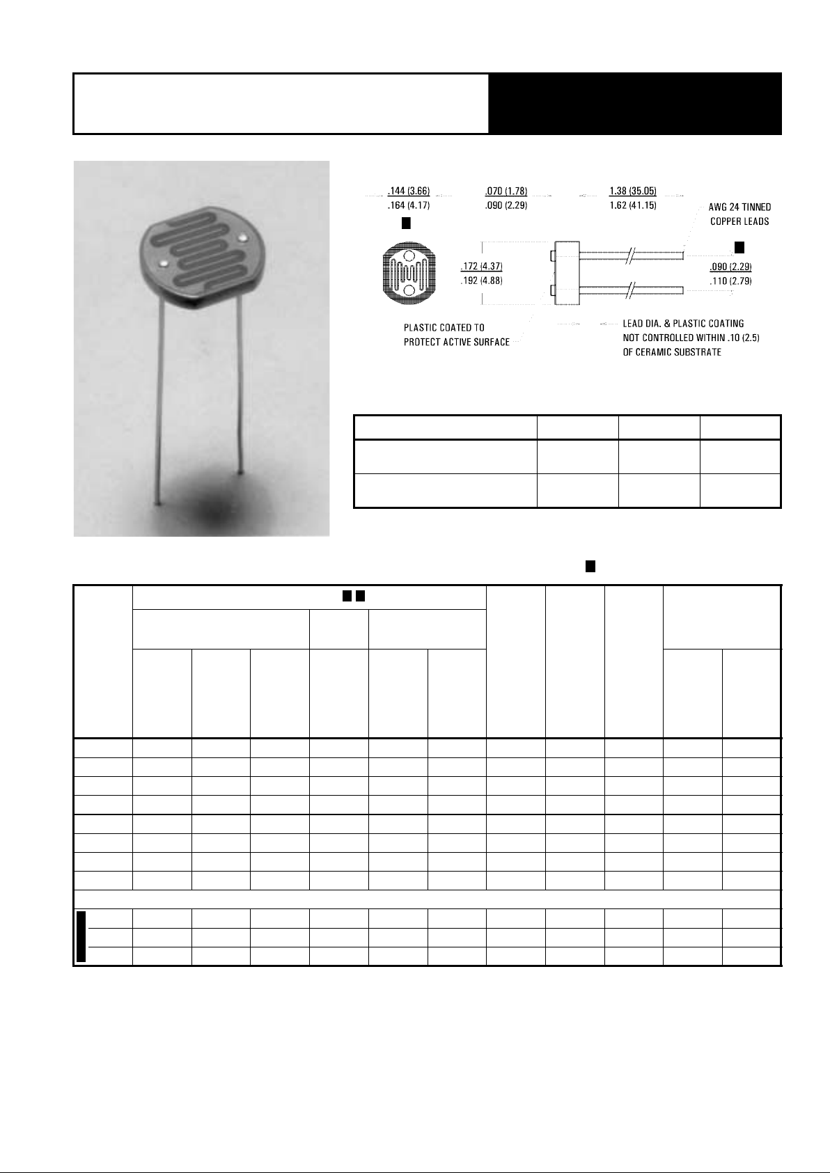
Photoconductive Cell VT900 Series
PACKAGE DIMENSIONS inch (mm)
ABSOLUTE MAXIMUM RATINGS
Parameter Symbol Rating Units
Continuous Power Dissipation
Derate Above 25°C
P
D
∆PD / ∆T
80
1.6
mW
mW/°C
Temperature Range
Operating and Storage T
A
–40 to +75 °C
2
5
ELECTRO-OPTICAL CHARACTERICTICS @ 25°C (16 hrs. light adapt, min.)
See page 13 for notes.
Part
Number
Resista nce (O hms)
Material
Type
Sensitivity
(γ, typ.)
Maximum
Voltage
(V, pk)
Response Time @ 1 fc
(ms, typ.)
10 lux
2850 K
2 fc
2850 K
Dark
Min. Typ. Max. Typ. Min. sec. Rise (1-1/e) Fall (1/e)
VT9ØN1 6 k 12 k 18 k 6 k 200 k 5 Ø 0.80 100 78 8
VT9ØN2 12 k 24 k 36 k 12 k 500 k 5 Ø 0.80 100 78 8
VT9ØN3 25 k 50 k 75 k 25 k 1 M 5 Ø 0.85 100 78 8
VT9ØN4 50 k 100 k 150 k 50 k 2 M 5 Ø 0.90 100 78 8
VT93N1 12 k 24 k 36 k 12 k 300 k 5 3 0.90 100 35 5
VT93N2 24 k 48 k 72 k 24 k 500 k 5 3 0.90 100 35 5
VT93N3 50 k 100 k 150 k 50 k 500 k 5 3 0. 90 100 35 5
VT93N4 100 k 200 k 300 k 100 k 500 k 5 3 0.90 100 35 5
VT935G
Group A 10 k 18.5 k 27 k 9.3 k 1 M 5 3 0.90 100 35 5
Group B 20 k 29 k 38 k 15 k 1 M 5 3 0.90 100 35 5
Group C 31 k 40.5 k 50 k 20 k 1 M 5 3 0.90 100 35 5
4
3 6
LOG (R10/R100)
LOG (100/10)
-------------------------------------
1
PerkinElmer Optoelectronics, 10900 Page Ave., St. Louis, MO 63132 USA Phone: 314-423-4900 Fax: 314-423-3956 Web: www.perkinelmer.com/opto
Page 20
15
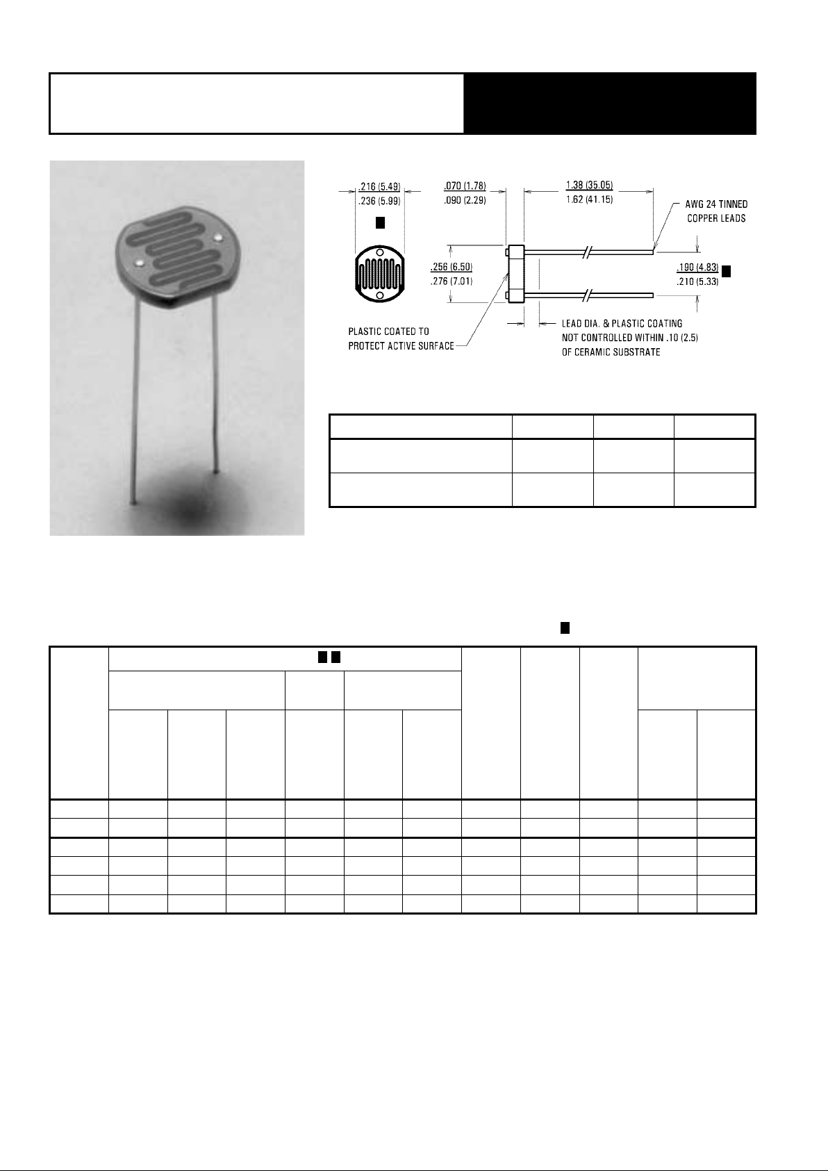
Photoconductive Cell VT 800 Ser ies
PACKAGE DIMENSIONS inch (mm)
ABSOLUTE MAXIMUM RATINGS
Parameter Symbol Rating Units
Continuous Power Dissipation
Derate Above 25°C
P
D
∆PD / ∆T
175
3.5
mW
mW/°C
Temperature Range
Operating and Storage T
A
–40 to +75 °C
2
5
ELECTRO-OPTICAL CHARACTERICTICS @ 25°C (16 hrs. light adapt, min.)
See page 13 for notes.
Part
Number
Resistance (Ohms)
Material
Type
Sensitivity
(γ, typ.)
Maximum
Voltage
(V, pk)
Response Time @ 1 fc
(ms, typ.)
10 lu x
2850 K
2 fc
2850 K
Dark
Min. Typ. Max. Ty p. Min. sec. Rise (1-1 /e) F all (1/e)
VT8ØN1 4 k 8 k 12 k 4 k 100 k 5 Ø 0.80 100 78 8
VT8ØN2 8 k 16 k 24 k 8 k 500 k 5 Ø 0.80 200 78 8
VT83N1 6 k 12 k 18 k 6 k 100 k 5 3 0.95 100 35 5
VT83N2 12 k 28 k 36 k 14 k 500 k 5 3 0.95 200 35 5
VT83N3 24 k 48 k 72 k 24 k 1 M 5 3 0.95 200 35 5
VT83N4 50 k 100 k 150 k 50 k 2 M 5 3 0. 95 200 35 5
4
3 6
OG (R10/R100)
LOG (100/10)
------------------------------------
PerkinElmer Optoelectronics, 10900 Page Ave., St. Louis, MO 63132 USA Phone: 314-423-4900 Fax: 314-423-3956 Web: www.perkinelmer.com/opto
Page 21
16
Dual Element Photoconductive Cell
VT800CT Series
PACKAGE DIMENSIONS inch (mm)
ABSOLUTE MAXIMUM RATINGS
Parameter Symbol Rating Units
Continuous Power Dissipation (Per Element)
Derate Above 25°C
P
D
∆PD / ∆T
80
1.6
mW
mW/°C
Temperature Range
Operating and Storage T
A
–40 to +75 °C
2
5
ELECTRO-OPTICAL CHARACTERICTICS @ 25°C (16 hrs. light adapt, min.)
See page 13 for notes.
Part
Number
Resistance Per Element (Ohms)
Matching
@ 10 Lux
R
1–2
/ R
2–3
Material
Type
Sensitivity
(γ, typ.)
Maximum
Voltage
(V, pk)
Response Time @ 1 fc
(ms, typ.)
10 lux
2850 K
2 fc
2850 K
Dark
Min. Typ. Max. Typ. Min. sec. Rise (1-1/e) Fall (1/e)
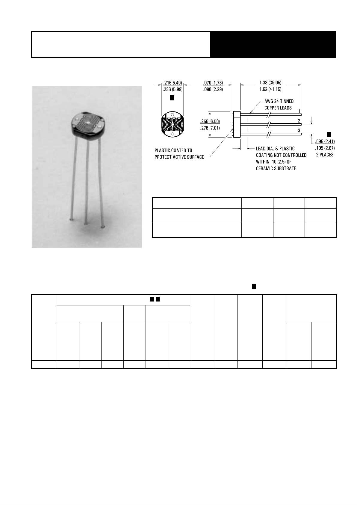
VT83CT 30 k 60 k 90 k 30 k 1 M 5 0.70 – 1.30 3 0.90 100 35 5
4
3 6
OG (R10/R100)
LOG (100/10)
------------------------------------
PerkinElmer Optoelectronics, 10900 Page Ave., St. Louis, MO 63132 USA Phone: 314-423-4900 Fax: 314-423-3956 Web: www.perkinelmer.com/opto
VT800CT Se ries
Page 22
17
Photoconductive Cell VT 400 Ser ies
PACKAGE DIMENSIONS inch (mm)
ABSOLUTE MAXIMUM RATINGS
Parameter Symbol Rating Units
Continuous Power Dissipation
Demand (20 minutes)
Derate Above 25°C
P
D
∆PD / ∆T
400
600
8.0
mW
mW
mW/°C
Temperature Range
Operating and Storage T
A
–40 to +75 °C
2
5
ELECTRO-OPTICAL CHARACTERICTICS @ 25°C (16 hrs. light adapt, min.)
See page 13 for notes.
Part
Number
Resistance (Ohms)
Material
Type
Sensitivity
(γ, typ.)
Maximum
Voltage
(V, pk)
Response Time @ 1 fc
(ms, typ.)
1 fc
6500 K
2 fc
2850 K
Dark
Min. Typ. Max. Ty p. Min. sec. Rise (1-1 /e) F all (1/e)
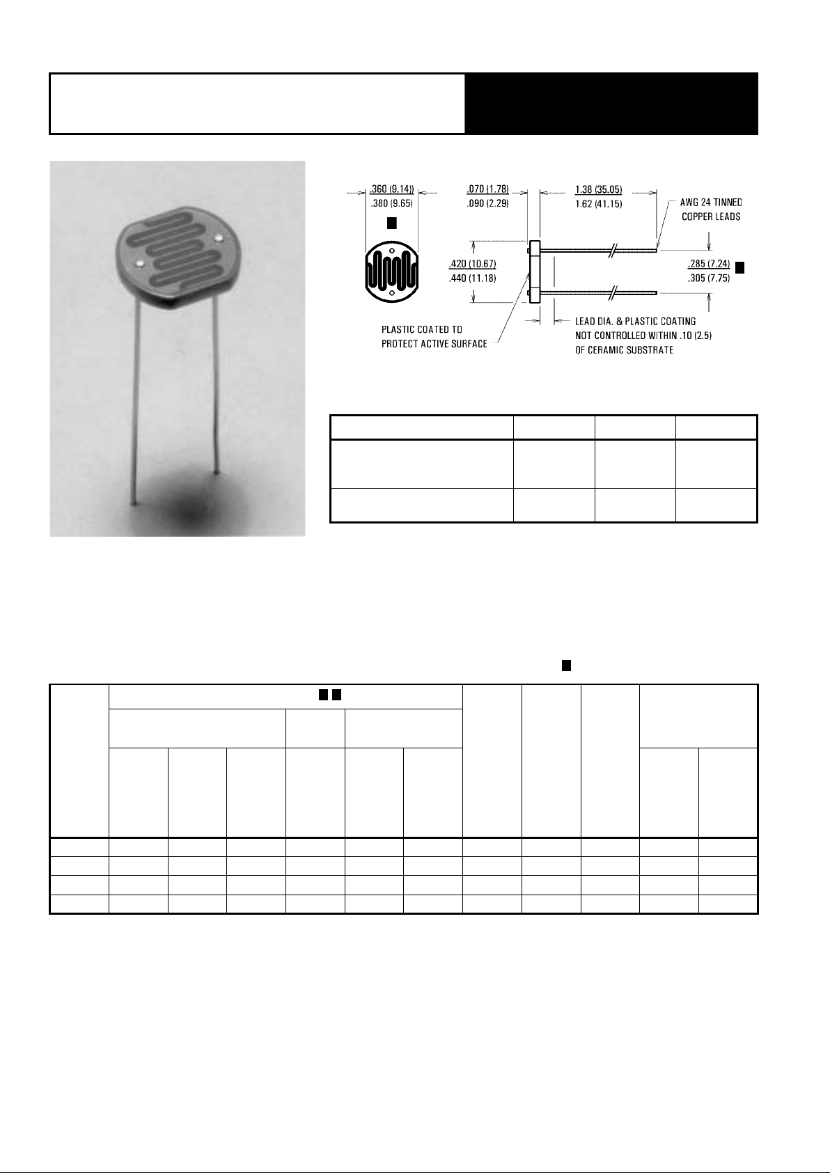
VT43N1 4 k 8 k 12 k — 300 k 30 3 0.90 250 90 18
VT43N2 8 k 16 k 24 k — 300 k 30 3 0.90 250 90 18
VT43N3 16 k 32 k 48 k — 500 k 30 3 0.90 400 90 18
VT43N4 33 k 66 k 100 k — 500 k 30 3 0.90 400 90 18
4
3 6
OG (R10/R100)
LOG (100/10)
------------------------------------
PerkinElmer Optoelectronics, 10900 Page Ave., St. Louis, MO 63132 USA Phone: 314-423-4900 Fax: 314-423-3956 Web: www.perkinelmer.com/opto
Page 23
18
Photoconductive Cell VT200 Series
PACKAGE DIMENSIONS inch (mm)
ABSOLUTE MAXIMUM RATINGS
Parameter Symbol Rating Units
Continuous Power Dissipation
Derate Above 25°C
P
D
∆PD / ∆T
50
1.0
mW
mW/°C
Temperature Range
Operating and Storage T
A
–40 to +75 °C
2
ELECTRO-OPTICAL CHARACTERICTICS @ 25°C (16 hrs. light adapt, min.)
See page 13 for notes.
Part
Number
Resista nce (O hms)
Material
Type
Sensitivity
(γ, typ.)
Maximum
Voltage
(V, pk)
Response Time @ 1 fc
(ms, typ.)
10 lux
2850 K
2 fc
2850 K
Dark
Min. Typ. Max. T yp. Min. sec. Rise (1 -1 /e) F all (1/e )
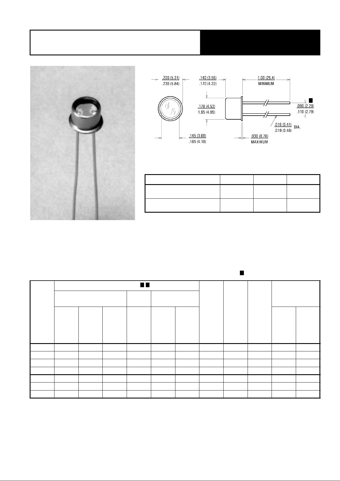
VT2ØN1 8 k 16 k 24 k 8 k 200 k 5 Ø 0.80 100 78 8
VT2ØN2 16 k 34 k 52 k 17 k 500 k 5 Ø 0.80 100 78 8
VT2ØN3 36 k 72 k 108 k 36 k 1 M 5 Ø 0.80 100 78 8
VT2ØN4 76 k 152 k 230 k 76 k 2 M 5 Ø 0.80 200 78 8
VT23N1 20 k 40 k 60 k 20 k 500 k 5 3 0.85 100 35 5
VT23N2 42 k 86 k 130 k 43 k 1 M 5 3 0.85 100 35 5
VT23N3 90 k 180 k 270 k 90 k 2 M 5 3 0. 85 100 35 5
4
3 6
LOG (R10/R100)
LOG (100/10)
-------------------------------------
PerkinElmer Optoelectronics, 10900 Page Ave., St. Louis, MO 63132 USA Phone: 314-423-4900 Fax: 314-423-3956 Web: www.perkinelmer.com/opto
Page 24
19
Photoconductive Cell VT 300 Ser ies
PACKAGE DIMENSIONS inch (mm)
ABSOLUTE MAXIMUM RATINGS
Parameter Symbol Rating Units
Continuous Power Dissipation
Derate Above 25°C
P
D
∆PD / ∆T
125
2.5
mW
mW/°C
Temperature Range
Operating and Storage T
A
–40 to +75 °C
2
ELECTRO-OPTICAL CHARACTERICTICS @ 25°C (16 hrs. light adapt, min.)
See page 13 for notes.
Part
Number
Resistance (Ohms)
Material
Type
Sensitivity
(γ, typ.)
Maximum
Voltage
(V, pk)
Response Time @ 1 fc
(ms, typ.)
10 lu x
2850 K
2 fc
2850 K
Dark
Min. Typ. Max. Ty p. Min. sec. Rise (1-1 /e) F all (1/e)
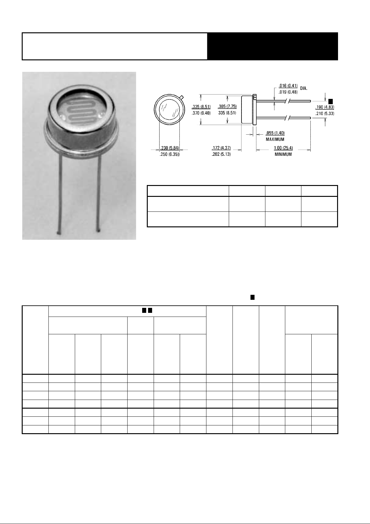
VT3ØN1 6 k 12 k 18 k 6 k 200 k 5 Ø 0.75 100 78 8
VT3ØN2 12 k 24 k 36 k 12 k 500 k 5 Ø 0.80 200 78 8
VT3ØN3 24 k 48 k 72 k 24 k 1 M 5 Ø 0.80 200 78 8
VT3ØN4 50 k 100 k 150 k 50 k 2 M 5 Ø 0.80 300 78 8
VT33N1 20 k 40 k 60 k 20 k 500 k 5 3 0.90 100 35 5
VT33N2 40 k 80 k 120 k 40 k 1 M 5 3 0.90 200 35 5
VT33N3 80 k 160 k 240 k 80 k 2 M 5 3 0. 90 200 35 5
4
3 6
OG (R10/R100)
LOG (100/10)
------------------------------------
PerkinElmer Optoelectronics, 10900 Page Ave., St. Louis, MO 63132 USA Phone: 314-423-4900 Fax: 314-423-3956 Web: www.perkinelmer.com/opto
Page 25
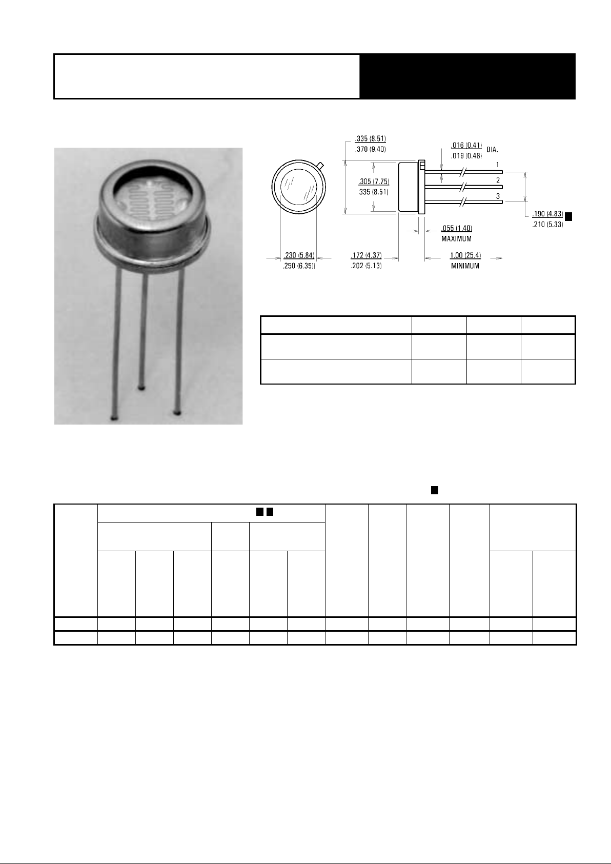
20
Dual Element Photoconductive Cell
VT300CT Series
PACKAGE DIMENSIONS inch (mm)
ABSOLUTE MAXIMUM RATINGS
Parameter Symbol Rating Units
Continuous Power Dissipation (Per Element)
Derate Above 25°C
P
D
∆PD / ∆T
50
1.0
mW
mW/°C
Temperature Range
Operating and Storage T
A
–40 to +75 °C
2
ELECTRO-OPTICAL CHARACTERICTICS @ 25°C (16 hrs. light adapt, min.)
See page 13 for notes.
Part
Number
Resistance Per Element (Ohms)
Matching
10 Lux
R
1–2
/ R
2–3
Material
Type
Sensitivity
(γ, typ.)
Maximum
Voltage
(V, pk)
Response Time @ 1 fc
(ms, typ.)
10 lux
2850 K
2 fc
2850 K
Dark
Min. Typ. Max. Typ. Min. sec. Rise (1-1/e) Fall (1/e)
VT3ØCT 10 k 20 k 30 k 10 k 500 k 5 0.70 – 1.30 Ø 0.80 200 78 8
VT33CT 60 k 120 k 180 k 60 k 1 M 5 0.70 – 1.30 3 0.90 200 35 5
4
3 6
OG (R10/R100)
LOG (100/10)
------------------------------------
PerkinElmer Optoelectronics, 10900 Page Ave., St. Louis, MO 63132 USA Phone: 314-423-4900 Fax: 314-423-3956 Web: www.perkinelmer.com/opto
VT300CT Series
Page 26
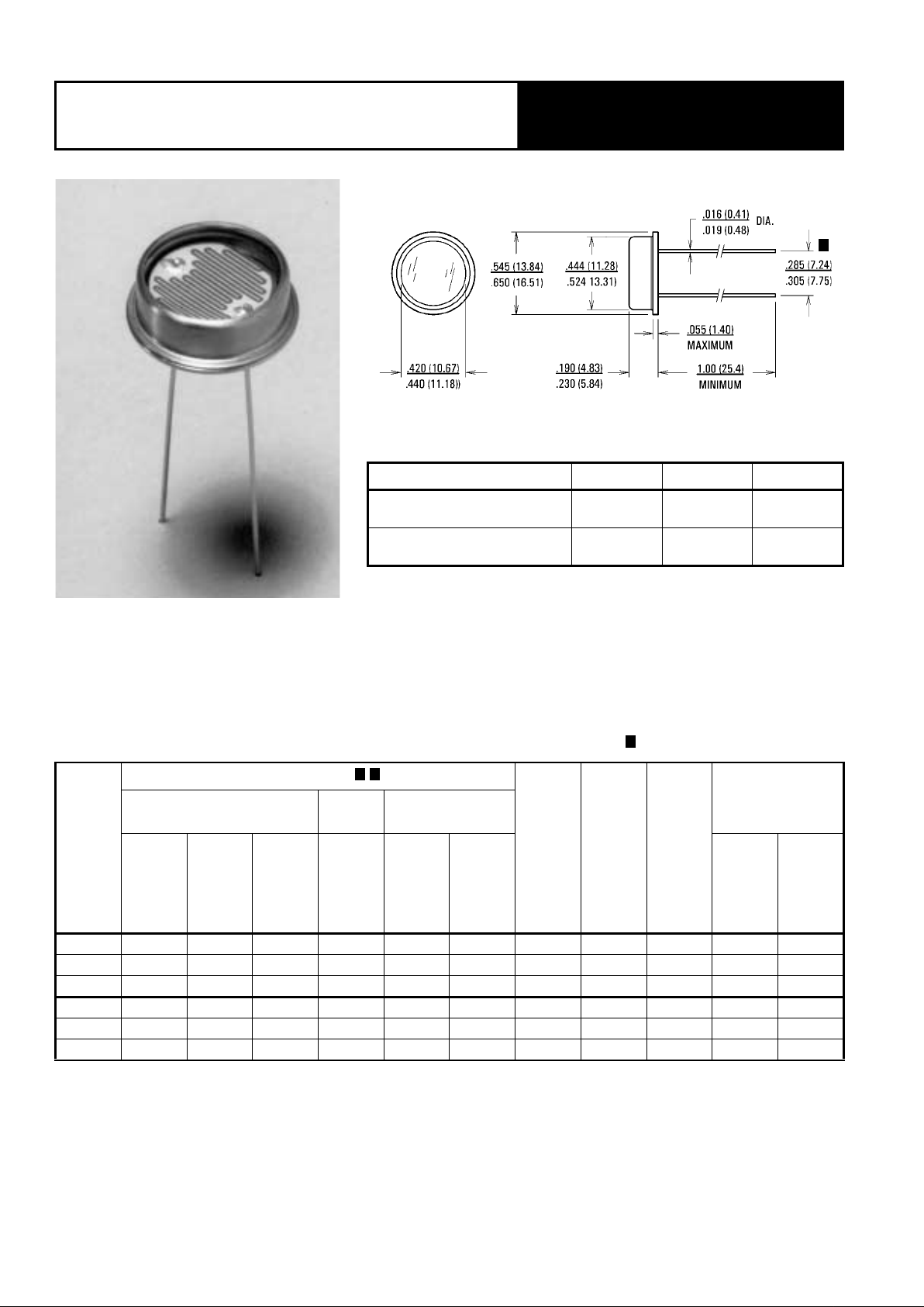
21
Photoconductive Cell VT 500 Ser ies
PACKAGE DIMENSIONS inch (mm)
ABSOLUTE MAXIMUM RATINGS
Parameter Symbol Rating Units
Continuous Power Dissipation
Derate Above 25°C
P
D
∆PD / ∆T
500
10
mW
mW/°C
Temperature Range
Operating and Storage T
A
–40 to +75 °C
2
ELECTRO-OPTICAL CHARACTERICTICS @ 25°C (16 hrs. light adapt, min.)
See page 13 for notes.
Part
Number
Resistance (Ohms)
Material
Type
Sensitivity
(γ, typ.)
Maximum
Voltage
(V, pk)
Response Time @ 1 fc
(ms, typ.)
10 lu x
2850 K
2 fc
2850 K
Dark
Min. Typ. Max. Ty p. Min. sec. Rise (1-1 /e) F all (1/e)
VT5ØN1 4 k 8 k 12 k 4 k 200 k 5 Ø 0.75 200 78 8
VT5ØN2 8 k 16 k 24 k 8 k 500 k 5 Ø 0.75 200 78 8
VT5ØN3 16 k 32 k 48 k 16 k 1 M 5 Ø 0.80 300 78 8
VT53N1 16 k 32 k 48 k 16 k 1 M 5 3 0.85 200 35 5
VT53N2 32 k 76 k 96 k 38 k 2 M 5 3 0.85 200 35 5
VT53N3 66 k 132 k 200 k 66 k 3 M 5 3 0. 85 300 35 5
4
3 6
OG (R10/R100)
LOG (100/10)
------------------------------------
PerkinElmer Optoelectronics, 10900 Page Ave., St. Louis, MO 63132 USA Phone: 314-423-4900 Fax: 314-423-3956 Web: www.perkinelmer.com/opto
Page 27
22
Application Notes—Photoconductive Cells
APPLICATION NOTE #1
Light - Some Physical Basics
Light is pr oduced by the r elease of energy from the atoms o f a material
when they are excited by heat, chemical reaction or other means. Light
travels through space in the form of an electromagnetic wave.
A consequence of this wave-like nature is that each “color” can be
completely defined by specifying its unique wavelength. The
wavelength is defined as the distance a wave travels in one cycle.
Since the wavelengths of light are very short they are normally
measured in nanometers, one nanometer being equal to 1 x 10
-9
meters.
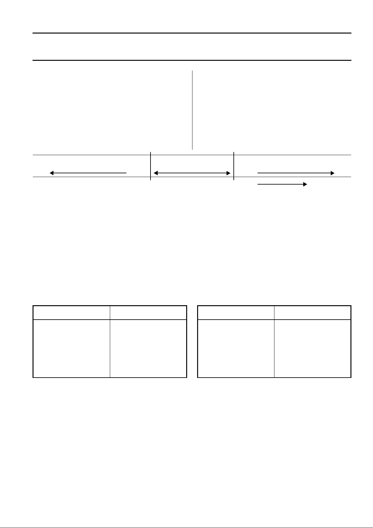
The spectral response of PerkinElmer’s photoconductors are specified
by lots of relative response versus wavelength (color) for various
mater ia l typ es .
Nat u ra l Il lu mina n c e Room Illumination
Ultraviolet
(To X-rays and Gamma Rays)
Infrared
(T o Radar Waves )
Visible Light
400
700
Violet Red Wavelength
Violet Below 450 nm
Blue 450 - 500 nm
Green 500 - 570 nm
Yellow 570 - 590 nm
Orange 590 - 610 nm
Red 610 - 700 nm
Sky Condition Light Level (T ypical )
Direct Sunlight 10000 fc
Overcast Day 1000 fc
Twilight 1 fc
Full Moon 0.1 fc
Clear Night Sky (moonless) 0.001 fc
Lighting Condition Light Level (Typical)
Candle - Lit Room 5 fc
Auditorium 10 fc
Classroom 30 fc
Inspection Station 250 fc
Hospital Operating Room 500 - 1000 fc
Page 28
23
Application Notes—Photoconductive Cells
APPLICATION NOTE #2
Light Resistance Measurement Techniques
The light resistance or “on” resistance (RON) of a photoconductor cell
is defined as the resistance of the cell as measured at a special light
level using a light source with a known output spectrum. Furthermore,
the cell must be “light adapted” for a specific period of time at an
established level of ill umination in order to achie ve repeatab le r esults.
The industry standard light source used for light resistance
measurements is a tungsten filament lamp operating at a color
temperatu re of 2850 K. Specifyi ng the 2850 K color tempera ture f or the
light source fi x es the spectr al output (i.e. the tungs ten f ilam ent light has
fixed amounts of blue, green, red, and infrared light).
For consistency and ease of comparing different cells, PerkinElmer
lists light resistance values for its photocells at two standard light
levels: 2 fc (footcandles) and at 10 lux. The footcandle is the old,
historical unit for measuring light intensity and is defined as the
illumination produced when the light from one standard candle falls
normally on a surface at a distance of on e foot. The lux (the m etric unit
of light measurement) is the illumination produced when the light from
one candle falls normally on a surface of one meter. The conversion
between f ootcandle and lux. is as f ollows:
1.0 fc = 10.76 lux
1.0 lux = 0.093 fc
As explained in the section on “Selecting a Photocell”, the “light
history” effect necessitates the pre-conditioning of the cell before a
light resistance measurement is made. PerkinElmer stores all cells at
room tempe r ature for 16 hours m inimum at 30 – 50 fc (about 320 - 540
lux) prior to making the test measurement.
Sometimes the design engineer or user does not have access to the
precision measurement equipment necessary to determine the light
levels or light intensities of the application. Should this prove to be a
problem, calibrated photocell samples with individual data can be
provided by PerkinElm er.
APPLICATION NOTE #3
Spectral Output of Common Light Sources
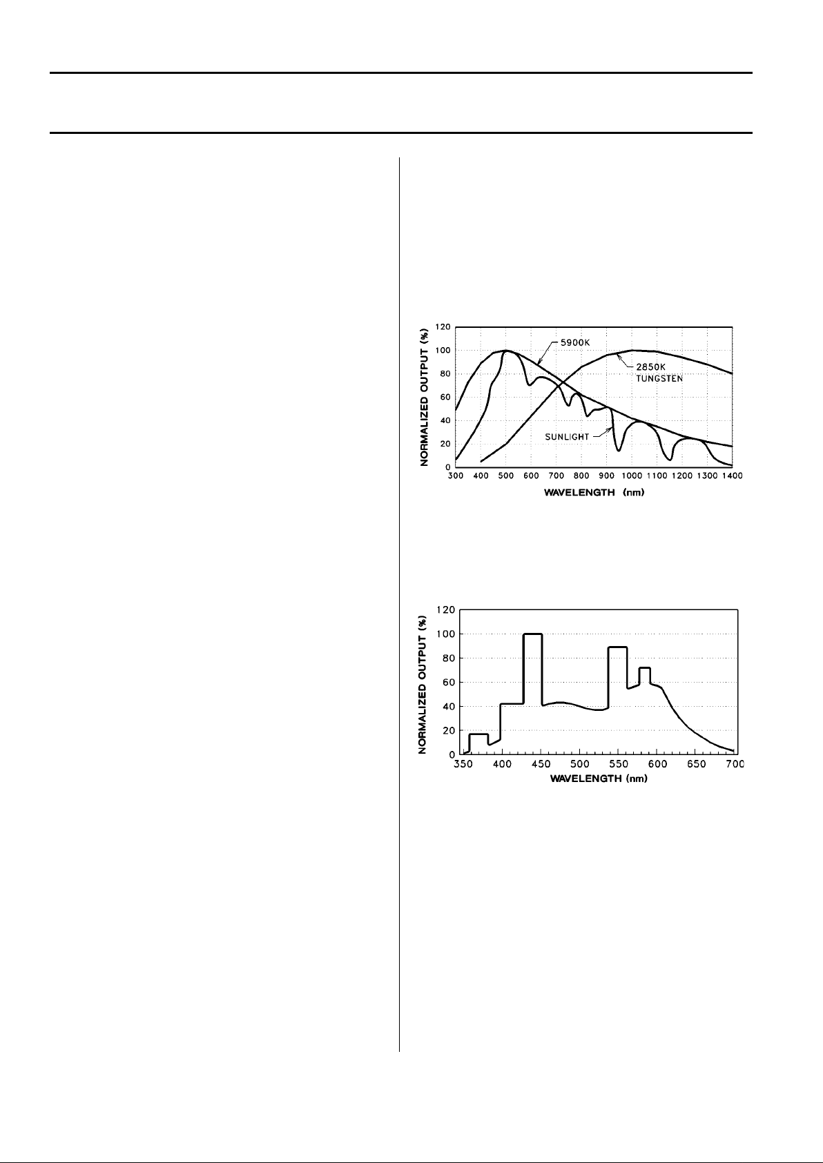
Incandescent lamps can be considered as black body radiators whose
spectral output is dependent on their color temperature. The sun has
approximately the sam e spectral radi ation distributi on as that of a black
body @ 5900 K. However, as viewed from the surface of the earth, the
sun's spectrum cont ains H
2
O and CO2 absorption bands .
Black Body Sources Output vs. Wavelength
Fluorescent lamps exhibit a broad band spectral output with narrow
peaks in certain parts of the spectrum. Shown below is a plot of the
light output of a typical daylight type fluorescent tube.
Fluorescent Lamp Output vs. Wavelength
Due to their long operating lifetimes, small size, low power
consumption, and the fact they generate little heat, LEDs are the light
sources of choice in many applications. When biased in the forward
direction LEDs emit light tha t is very narrow in spectral bandwidth (light
of one color). The “color” of the light emitted depends on which
semiconductor material was used for the LED.
Page 29
24
Application Notes—Photoconductive Cells
LED Light Sources
APPLICATION NOTE #4
Spectral Matching of LEDs and
Photoconductive T ypes
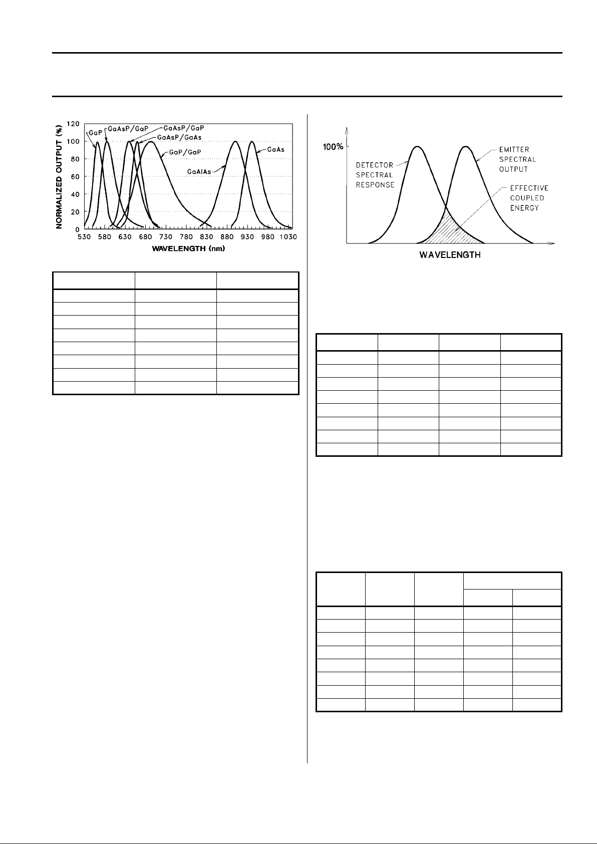
Since light sources and light detectors are almost always used
together the designer must take into consideration the optical coupling
of this system or the ability of the detector to “see” the lig ht source.
In order to have good optical coupling between the emitter and the
conductor the spectral output of the light source must, to some degree ,
overlap t he spectral response of t he detector. If the design involves the
use of a light source with a broad band spectral output the designer is
assured that the photocell will have good response to the light. This
may not be the case when an LED light source is employed. LEDs em it
their light within a very narrow spectral band so that they are often
considered to be emitting at only on (peak) wavelength.
Spectral matching factors were calculated for a number of different
LEDs and the photoconductor material types manufactured by
PerkinElmer. Each matching factor was derived by multiplying the
detector response curves by the LED spectral output curve and then
measuring the re sulting area.
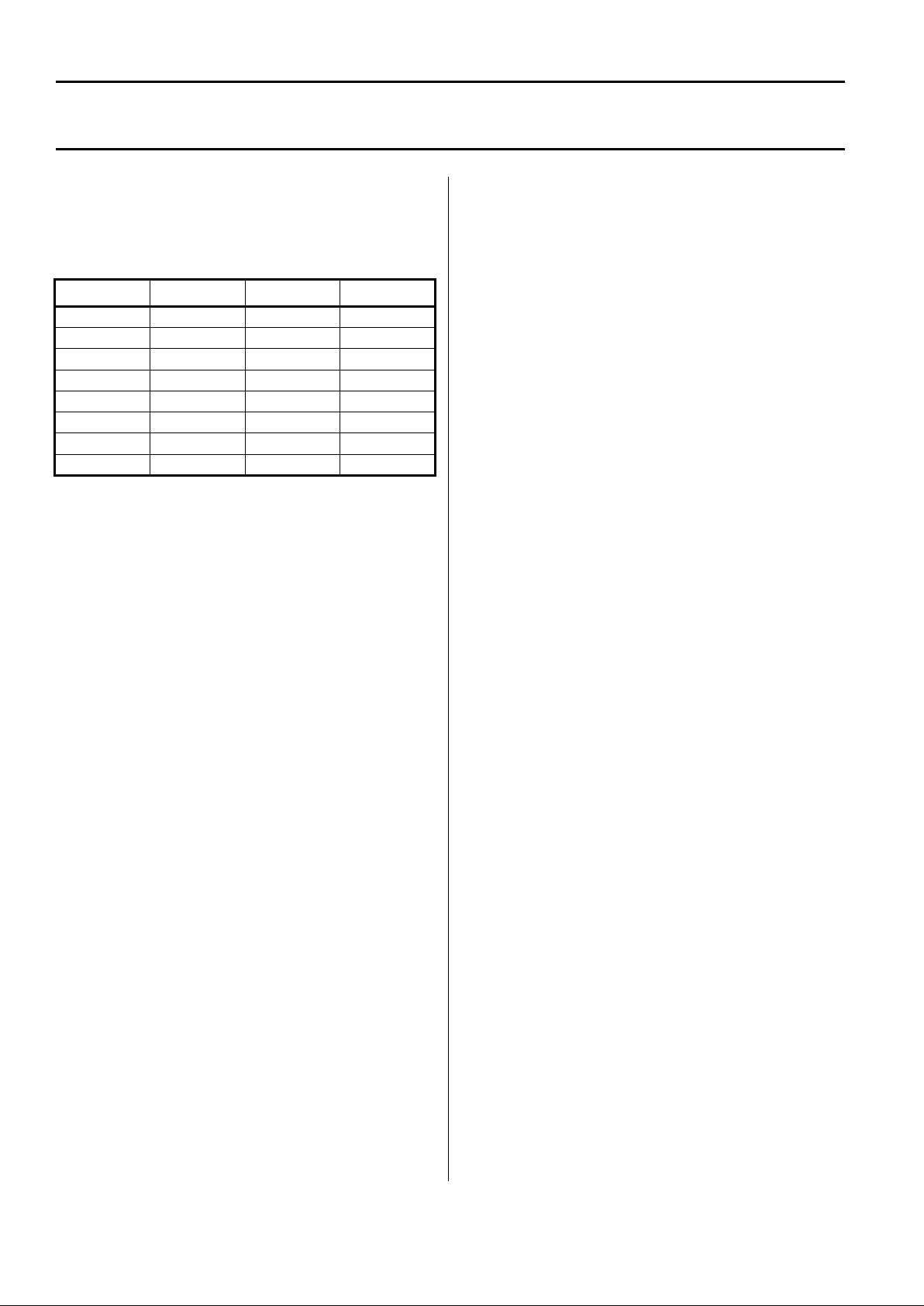
The LED/photocell matching factors listed are independent of power
output from the LEDs. In order to get a real feel on how well any LED/
photocell pair couple together, the power output from the LED at a
particular fo rward drive current must be considered.
Normalized LED/Photocell Matching
The intensit y of the light being emitted by visible LEDs is often given in
units of millicandela. Millicandela is photometric unit of measure which
assumes the hum an eye as the detector . For most detectors other th an
the human eye the most convenient system for measurement is the
radiometric system. Listed below is the typical light power output of
some LEDs measu red at two different forward dri ve currents. Note that
LEDs of a given type can show a 5:1 manufacturing spread in power
outputs.
LED Type Color λ
P
GaP GREEN 569 nm
GaAsP/GaP YELLOW 585 nm
GaAsP/GaP ORANGE 635 nm
GaAsP/GaAs RED 655 nm
AIGaAs RED 660 nm
GaP/GaP RED 697 nm
GaAIAs INFRARED 880 nm
GaAs INFRARED 940 nm
LED Type λP (nm) Type Ø Material Type 3 Material
GaP 569 39% 40%
GaAsP/GaP 58 60% 52%
GaAsP/GaP 635 49% 38%
GaAsP/GaAs 655 31% 27%
AIGaAs 66 31% 27%
GaP/GaP 697 47% 31%
GaAIAs 880 — —
GaAs 940 — —
LED Type Color λ
P
(nm)
Power Output
I
f
= 1 mA If = 10 mA
GaP GREEN 569 nm 1.2 µW 24.1 µW
GaAsP/GaP YELLOW 585 nm 0.3 µW 26.2 µW
GaAsP/GaP ORANGE 635 nm 3.2 µW 101.9 µW
GaAsP/GaAs RED 655 nm 6.2 µW 102.1 µW
AIGaAs RED 660 nm 33.8 µW 445.1 µW
GaP/GaP RED 697 nm 54.3 µW 296.2 µW
GaAIAs INFRARED 880 nm 76.8 µW 1512.3 µW
GaAs INFRARED 940 nm 35.5 µW 675.0 µW
Page 30
25
Application Notes—Photoconductive Cells
Factoring in the power outputs of the LEDs, in this case at a forward
drive current of 10 ma, coupling factors (matching factor multiplied by
power output) for the various LED/material type combinations can be
generated.
Normalized LED/Photocell Coupling Factors @ 10 mA
Once gain, this data is intended as a general guide. LED power
outputs can vary 5:1 between manufacturer lots.
APPLICATION NOTE #5
Assembly Precautions
When soldering the cell leads take all measures possible to limit the
amount of heating to the photocell. The maximum recommended
soldering temperature is 250°C with a solder duration of 5 seconds.
Heat sink the LEDs if possible. Keep soldering iron 1/16 inch (1.6 mm)
minimum from base of package when soldering.
Avoid chemicals which can cause metal corrosion. Do not clean the
plastic coated cells with organic solvents (ketone types). Check with
factory for specific cleaning r ecomm endations.
Finally refrain from storing the cells under high temperature and/or
humidity conditions. If cells are stored in the dark for any length of time
please “lig ht adept” before testing (see section on Light Hi sto ry Eff ect).
Storage in the dark will change both the sensitivity and decay time of
the cell.
APPLICATION NOTE #6
A Low Cost Light Source for Measuring
Photocells
T
he Light Source used in the measurement of photocell resistance
must be characterized for intensity and spectral composition.
PerkinElmer uses a tungsten filament lamp having a spectral output
approximating a black body @ 2850 K with a known candlepower
output at a speci fied voltage and current.
While calibrated lamps of this type are available from the National
Institute of Standards and Technology (formerly NBS) and private
testing labs, a low cost alternative is to use a 100 W, inside frosted,
tungsten filament lamp available from any home or hardware store.
Such a lamp operated at 120 VAC will produce approximately 90
candlepower (cp) of illumination and a color temperature of 2700 K to
2800 K.
The relationship between candlepower and footcandle is:
Since this equation assumes a point source of light, the distance
between lamp and detector should be at least five times the lamp
diameter.
There are some characteristics of incandescent lamps which should
be noted:
1. Color temperat ure increases with increasing wattage.
2. When operated at a constant current, ligh t out put rises with time.
LED Type λP (nm) Type Ø Type 3
GaP 569 3% 3%
GaAsP/GaP 58 5% 5%
GaAsP/GaP 635 17% 13%
GaAsP/GaAs 655 11% 9%
AIGaAs 66 47% 35%
GaP/GaP 697 47% 31%
GaAIAs 880 — —
GaAs 940 — —
footcandle
candle power
distance in feet()
2
----------------------------------------=
Page 31

26
Application Notes—Photoconductive Cells
APPLICATION NOTE #7
How to Specify a Low Cost Photocell
Sometimes the demands of the application such as power dissipation,
“on” resistance, voltage, tem per ature coefficient, etc. limit the selection
of the photocell to one particular device. Howe ver, more common is t he
case where any number of photocell types can be used, especially if
minor changes are undertaken at an early enough point in the circuit
design. In these cases, price is often the deciding factor.
Many factors influence price. In order to give some guidance and
weight to these factors the reader is referred to the following table
which is meant to serve as a general guide.
Lower Cost Factor Higher Cost
Plastic Packaging Glass/Metal
Broad Resistance Range Narrow
Small Package Size Large
Open Order with
Scheduled Releases
Scheduling Released Orders
Standard Tests Testing Special Tests
Page 32
Analog Optical Isolators VACTROLS®
Page 33
28
What Are Analog Optical Isolators?
PerkinElmer Optoelectronics has been a leading manufacturer of
analog op ti cal isolators for over twenty years and makes a broad range
of standard pa rts under its trademark VACTROL®.
There are many kinds of optical isolators, but the most common is the
LED/phototransistor type. Other familiar types use output elements
such as light sensitive SCRs, Triacs, FETs, and ICs. The major
application for these silicon based devices is to provide electrical
isolation of digital lines connected between different pieces of
equipment. The principle of operation is very simple. When an input
current is applied to the LED, the output phototransistor turns on. The
only connection between the LED and phototransistor is through
light—not electricity, thus the term optical isolator. These optical
isolator s ar e pr imarily digital in nat ur e with fast response times suitable
for interfacing with logic gates. Rise and fall times of a few
microseconds, faster for som e isol ators, are typical.
The analog optical isolator (AOI) also uses an optical link between
input and output. The input element is an LED and the output element
is always photoconductive cell or simply photocell. Together, the
coupled pair act as an electrically variable potentiometer. since the
output element of the AOI is a resistor, the voltage applied to this
output resistor may be DC and/or AC and the magnitude may be as
low as zero or as high as the maximum voltage rating. Because the
input will control the magnitude of a complex waveform in a
proportional manner, this type of isolator is an analog
cont r ol el ement .
AOIs may be used in the ON-OFF mode but the fastest response time
is only in the millisecond range. A level sensitive Schmitt trigger is
required between the AOI and logic gates when used in digital circuits.
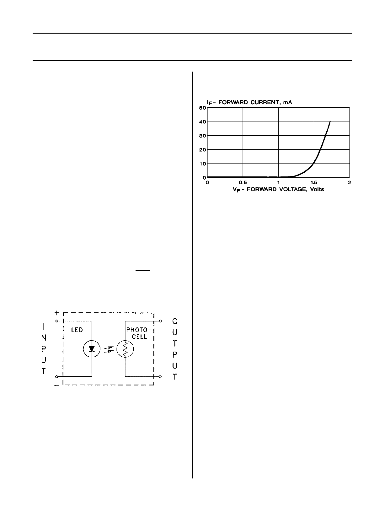
The figur e below shows the circuit diagram of a standard AO I.
AOI Circuit Diagram
Input Elem ent
Light emitting diodes used in AOIs are usually visible LEDs best
matching the sensitivity spectrum of the photocell output element.
LEDs are the ideal input element in most applications. They require
low drive current and voltage, respond very fast and have virtually
unlimited life. They are very rugged and are unaffected by shock and
vibration. Since the LED is a diode, it conducts in one direction only.
They must be protected from excessive forward current due to the low
dynamic resistance in the forward direction. The forward characteristic
of an LED typicall y used in VA CTROLs is shown below.
LED Forward Characteristics
Output Element
The output element in all PerkinElmer’s AOIs is a light dependent
resistor (LDR), also called a photoconductor or photocell. Photocells
are true resistors .
These passive resistors are made from a light sensitive polycrystalline
semiconductor thin film which has a very high electron/photon gain.
There are no P/N junctions in a photocell, making it a bilateral device.
The resistance of the photocell depends on the amount of light falling
on the cell. For a given illumination, the amount of electrical current
through the cell depends on the voltage applied. This voltage may be
either AC or DC. Thus, the photocell is the ideal low distortion output
element for an analog optoisolator.
A complete discussion of photoconductive cells can be found in the
first section of this book.
Page 34
29
What Are Analog Optical Isolators?
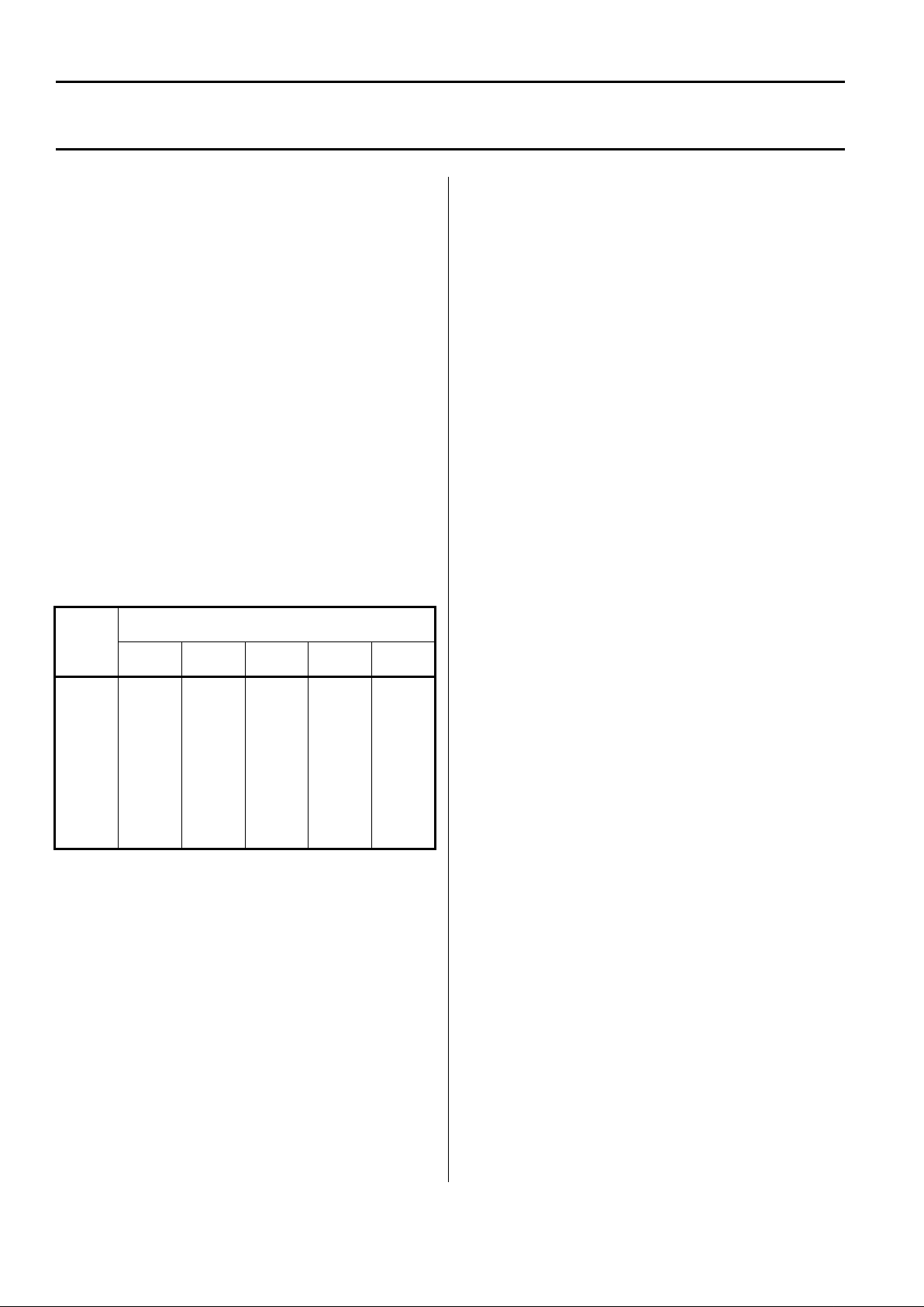
Light History Considerations
Photoconduct ive cells ex hibi t a phenomenon kno ws as hyst eresi s, ligh t
memory, or light history effect. Special consideration must be given to
this characteristic in the analog optoisolator because the
photoconductive element is normally in the dark. This will lead to
having the photocell initially in a “dark adapted” state in many
conditions.
The light levels that are seen by the photocell in many analog
optoisolator applications are quite low, ranging from 0.1 to 1.0 fc. The
effect of this combination of dar k adapt and low light levels wi ll be seen
in the fo llowi n g t a ble.
The table shows the relationship between light history and light
resistance at various light levels for different m aterial types. Th e values
shown were determined by dividing the resistance of a given cell,
following “infinite” light history (R
LH
), by the resistance of the same cel l
following infinite dark history (RDH). For pr actical purposes, 24 hours i n
the dark will achiev e RDH or 24 at approximately 30 fc will achieve RLH.
Variation of Resistance with Light History Expressed as a
Ratio R
LH/RDH
at Various Test Illumination Levels
The table illustrates the fact that the resistance of a photocell can
increase subst antially as it transit ions from dark adapted sta te to a light
adapted state. The table shows that the Type 1 photocell can increase
resistance by a factor of more than three times as it light adapts up to
0.1 fc. In some applications, this can be an important consideration. In
general, the magnitude of this effect is larger for types 1, 4, and 7 than
for types Ø, 2, and 3.
Each specific material type represents a tradeoff between several
characteristics. Selecting the best material is a process of determining
what characteristics are most important in the application. The chart
gives some appreciation for the general interrelationships between the
material types and their properties.
Material
Type
Illumination (fc)
0.01 0.1 1.0 10 100
Type Ø 1.60 1.40 1.20 1.10 1.10
Type 1 5.50 3.10 1.50 1.10 1.05
Type 2 1.50 1.30 1.20 1.10 1.10
Type 3 1.50 1.30 1.20 1.10 1.10
Type 4 4.50 3.00 1.70 1.10 1.10
Type 7 1.87 1.50 1.25 1.15 1.08
Page 35
30
What Are Analog Optical Isolators?
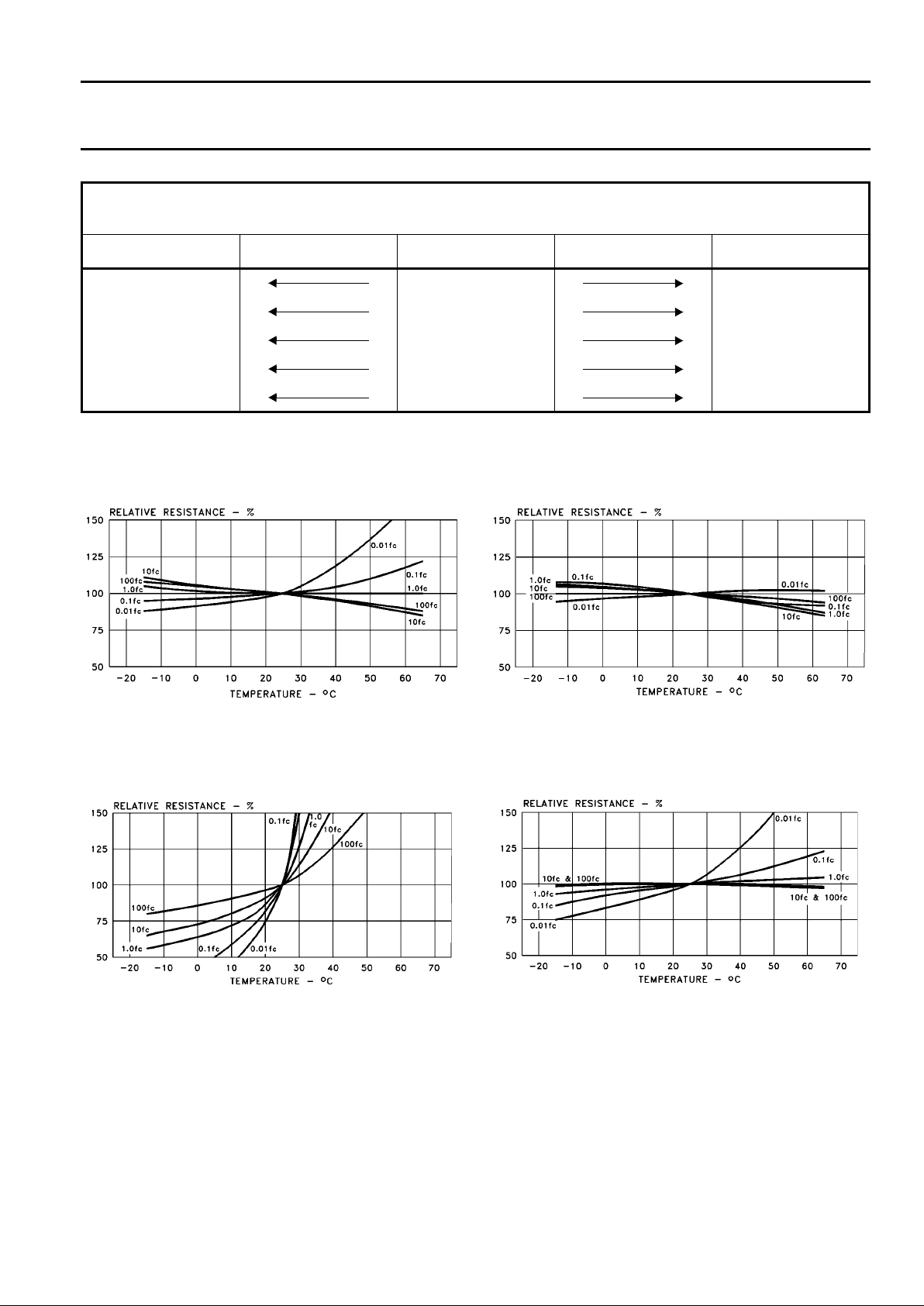
Relative Resistan ce vs. Temperature
Type Ø Material
Relative Resistan ce vs. Temperature
Typ e 1 Material
Relative Resistance vs. Temperature
Typ e 2 Material
Relative Resistance vs. Temperature
Typ e 3 Material
Material Characteristics
(General Trends)
Types 2 & 3 Type Ø Type 7 Type 4 Type 1
Lower Temperature Coefficient Higher
Higher Sheet Resistivity Lower
Slower Speed of Response Faster
Lower Resistance Slope Higher
Smaller Light History Effect Larger
Page 36
31
What Are Analog Optical Isolators?
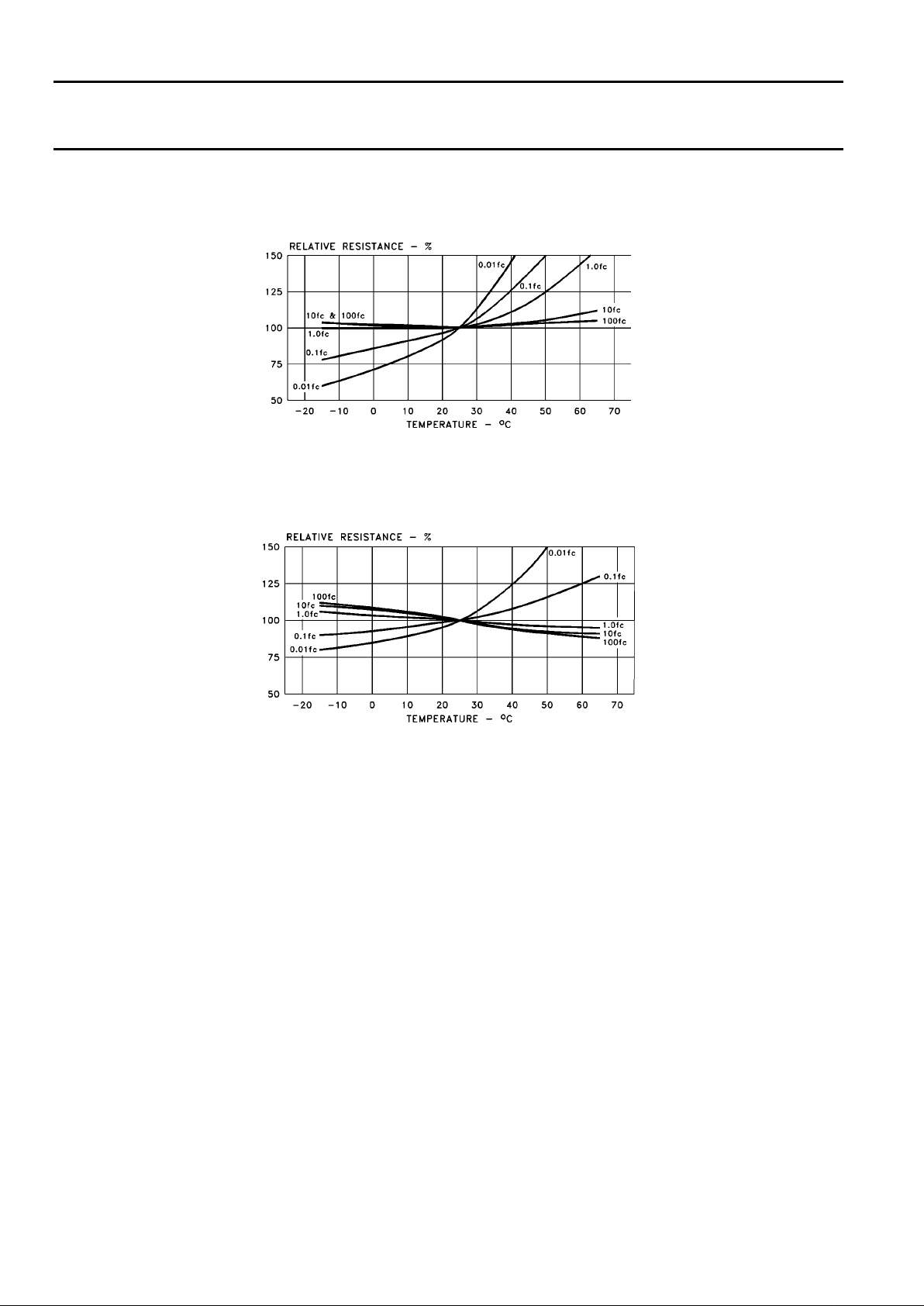
Relative Resistan ce vs. Tempera ture
Type 4 Materi al
Relative Resistan ce vs. Tempera ture
Type 7 Materi al
Page 37

32
Typical Applications of Analog Optical Isolators
Why Use Analog Optical Isolators?
PerkinEl mer O pt oelec tr oni cs’ lin e o f an alog op tic al i sol ato rs (AOIs) con sis ts o f a lig ht tigh t p ackage whi ch h ouse s a lig ht source and
one or more photoconductive cells. Through control of the input current or voltage applied to the AOI, the output resistance can be
varied. The output resistance can be made to switch between an “on” and “off ” state or made to track the input signal in an analog
manner. Beca use a smal l chang e in inpu t signal can cause a large cha nge in ou tput res ist ance, AOIs have been found to prov ide a
very economic and technically superior solution for many applications. Their general characteristics and salient features can be
summarized as follows:
• Hig h input-to- output v ol tage isolat ion
• True resistance elemen t o ut put
• Sin gle or dual element out puts availab l e
• Low cost
• Sui t able for AC or DC use
• Wide range of i nput to output charac teristics
• Low drive current
• Low “on” resistance, high “off” resistance
• Complete solid-state constructio n
Applications
Analog Optica l Iso lators are used in many d ifferen t types of cir cuits an d appl icat ions. H ere is a l ist of on ly a few exampl es of wh ere
AOIs have been used.
• DC isolators
• Feedback elements in automatic gain control circuits
• Audio limiting and compression
• Noiseless switching
• Logic interfacing
• Remote gain control for amplifiers
• Photochoppers
• Noiseless potentiometers
Page 38
33
Typical Applications of Analog Optical Isolators
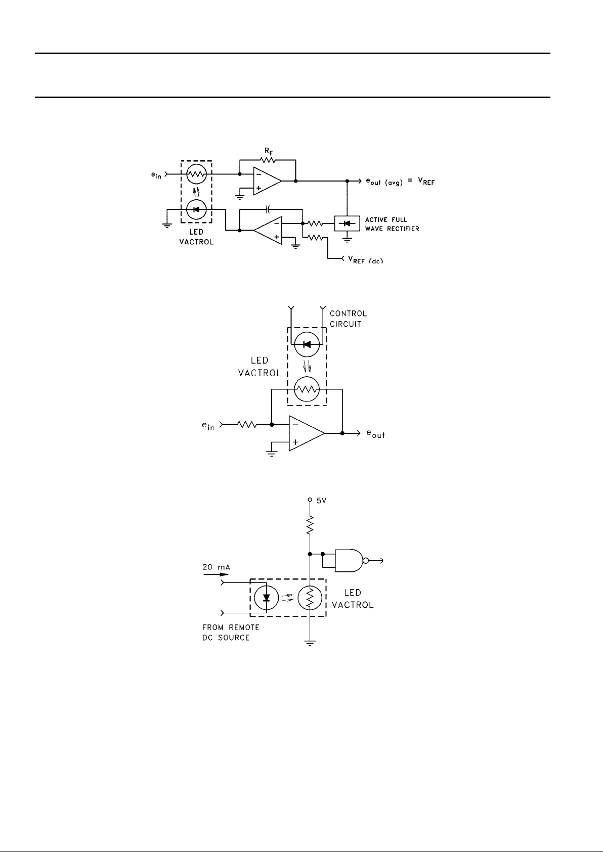
Typical Applicatio n Circuits
Automatic Gain Control (AGC)
Remote Gain Control
Noiseless Switching/Logic Interfacing
(See Application Note #1)
Audio Applications
Page 39
34
Characteristics of Analog Optical Isolators
Transfer Characteristics
The light output of an LED is proportional to the input drive current, IF.
Some LEDs will begin to radiate useful amounts of light output at
forward currents as low as 10 µA. These same LEDs can be driven at
50 mA with no degradation in performance.
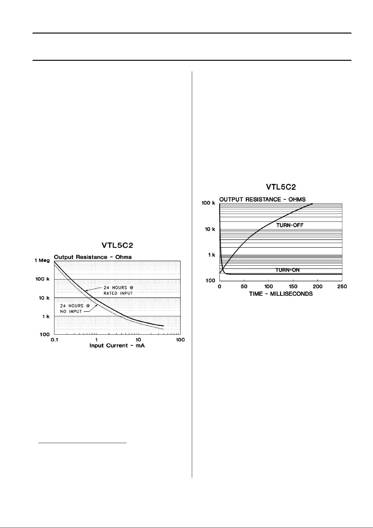
A transfer curve of output resistance versus input light current for a
typical AOI is shown in Figure 1. AOIs not only possess a large
dynamic range, but the output resistance tracks the input current in a
somewhat linear manner over a range of two or more decades.
This characteristic makes the AOI suitable for use in a very broad
range of applications, especially in audio circuits where they are used
for switching, limiting, and gating. For a more extensive discussion on
AOIs in audio circuits, refer to Application Notes #1.
Response Time
AOIs are not high speed devices. Speed is limited by the response
time of the photocell. With rise and fall times on the order of 2.5 to
1500 msec, most AOIs have bandwidths between 1 Hz and 200 Hz.
Figure 1. Transfer Curves (25°C)
One of the characteristics of photocells is that their speed of response
increases w it h increasing levels of illumination
.1
Thus the bandwidth of
Vactrols is somewhat dependent upon the input drive level to the LED.
In general , th e higher the input drive the w ider the bandwidth.
The turn-off time and turn-on time of photocells are not symmetrical.
The turn-on time can be an order of magnitude faster than the turn-off
time. In the dark (no input), the resistance of the cell is very high,
typically on the order of several megohms. When light is suddenly
applied, the photocells resistance drops very fast, typically reaching
63% (1-1/e conduct ance) of its final val ues in under 10 msec.
When the light is removed, the resistance increases initially at an
exponential rate, approximately tripling in a few milliseconds. The
resistance then increases linearly with time .
The fast turn-on and slow turn-off characteristics can be used to
advantage in many applications. This is especially true in audio
applications where a fast turn-on (attack) and a slow turn-off (release)
is preferred. For example, the typical AOI can be made to turn-on in
100 to 1000 µsec. In a limited circuit this is fast enough to catch high
peak amplitudes but not so fast as to cause obvious cli pping. The turnoff will tak e as much as 100 times longer so the audio circuit will return
to a normal gain conditi on wi thout a disturbing “thu mp ” in the speaker.
Figure 2. Resistance vs. Time
Noise
The sources of electrical noise in the output element of AOIs are the
same as for any other type of resistor.
One source of noise is thermal noise, also known as Johnson or
“white” noise, which is caused by the random motion of free electrons
in the photocond uctive material.
1. For a more comprehensive discussio n on the turn-on and turnoff characteristics of photocells and how response time is effected by light level, see the Photoconductive Cell section of this catalog.
Page 40

35
Characteristics of Analog Optical Isolators
Some major characteristics of Johnson noise are that it is:
1. Independ ent of frequency and contains a const ant power density
per unit of bandwi dth.
2. Temperature dependent , in cre asing with increased temper ature.
3. Dependent on photocell resistance value.
Johnson noise is defined by the following equati on:
where:
I
NJ
= Johnson noise curre nt, amps RMS
k = Boltzmann’s constant, 1.38 x 10
-23
T = temperature, degrees Kelvin
R = photocell resi stance
BW = bandwidt h of interest, Hertz
A second type of noise is “shot” noise. When a direct current flows
through a devi ce, these are some random variations superimposed on
this current due to random fluctuations in the emission of electrons due
to photon absorption. The velocity of the electrons and their transit
time will also have an effec t.
“Shot” noise i s:
1. Independent of frequency.
2. Dependent upon the direct current flowing through the photocell.
Shot noise is defined by the following equati on:
where:
I
NS
= shot noise current, amps RMS
e = electron charge, 1.6 x 10
-19
Idc = dc current, amps
BW = bandwidt h of interest, Hertz
The third type of noise is flicker of 1/f noise. The source of 1/f noise is
not well understood but seems to be attributable to manufacturing
noise mechanism s. Its equation is as follows:
where:
I
NF
= flicke r nois e, amps
K = a constant that depends on the type of material
and its geometry
Idc = dc current, amps
BW = bandwidth of interest, Hertz
f = frequency, Hertz
Unlike thermal or shortnoise, flicker noise has 1/f spectral density and
in the ideal case for which it is exactly proportional to , it is
termed “pink noise”. Unfortunately, the constant (K) can only be
determined empirically and may vary greatly even for similar devices.
Flicker noise may dominate when the bandwidth of interest contains
frequencie s less t han about 1 kHz.
In most AOI circuits noise is usually so low that it is hardly ever
considered. One notable exception is in applications where large
voltages are placed across the cell. For a typical isolator, it takes 80 to
100V across the photocell before the noise level starts to increase
significantly.
Distortion
Analog Optical Isolators have found wide use as control elements in
audio circu it s because they possess two characteri st ics w hich no other
active semiconductor device has: resistance output and low harmonic
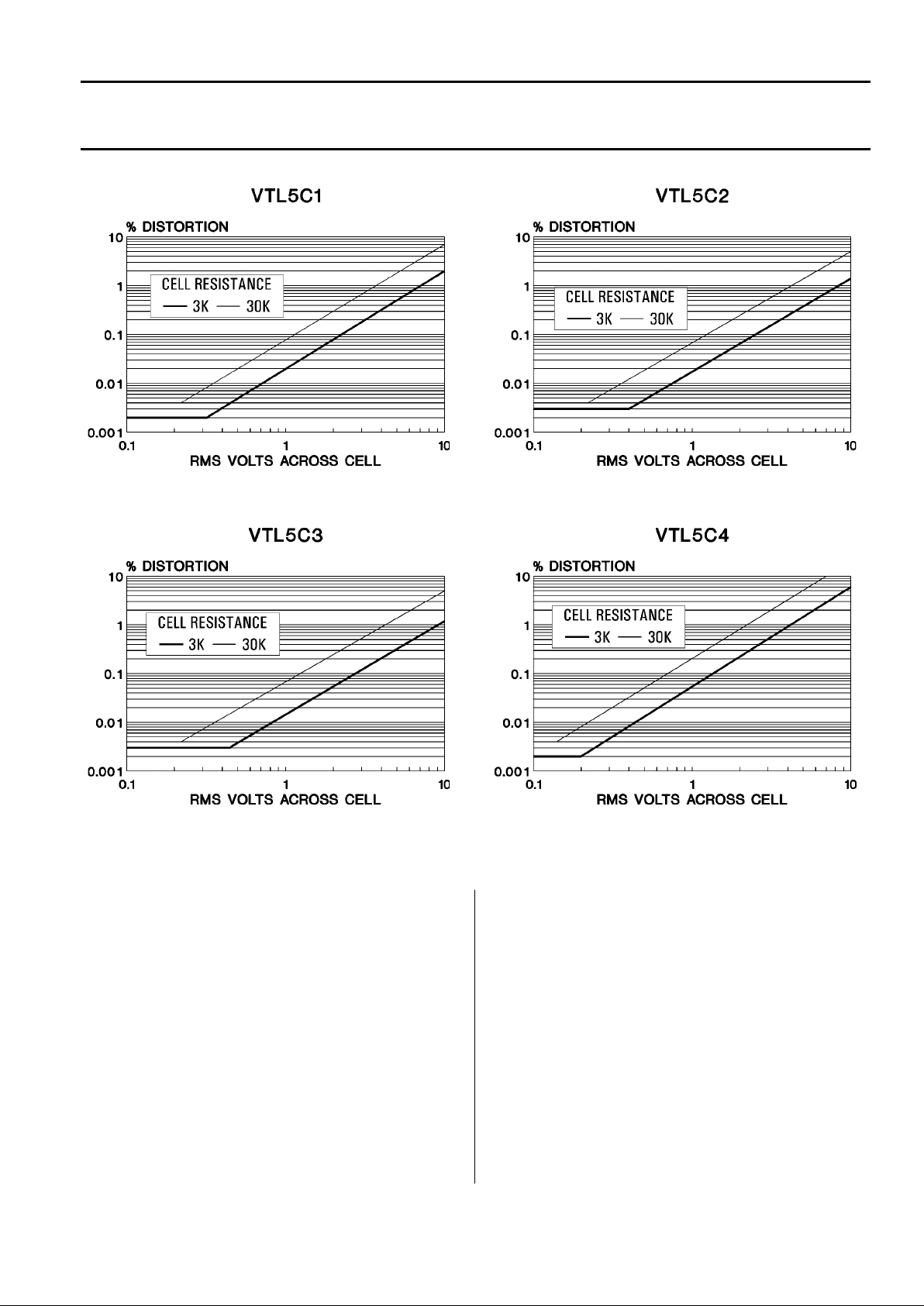
distortion. AOIs often exhibit distortion levels below -80 db when the
voltage applied to the photocell out put is kept below 0.5V.
Figure 3 shows the typical distortion generated in typical AOIs. The
distortion depends on the operating resistance level as well as the
applied voltage. The minimum distortion or threshold distortion shown
in Figure 3 is a second harmonic of the fundamental frequency. The
actual source of this distortion is unknown, but may be due to some
type of crossover nonlinearity at the original of the I-V curve of the
photocell.
I
NJ
4kTBW()R⁄=
I
NS
2eIdcBW=
I
NF
KIdcBW f⁄=
1f⁄
Page 41
36
Characteristics of Analog Optical Isolators
Figure 3. Typical LED AOI Distortion Characteristics
At high AC voltages, distortion to the waveform can be seen using an
oscilloscope. The waveform is still symmetrical but contains the
fundamental and the odd harmonics, the third harmonic being
predominant. If there is DC as well as AC voltage on the photocell,
both even and odd harmonics are generated.
The RMS value of voltage or current is not ver y sensitive to a large
third harmonic component, but the instantaneous value is. A 10%
harmonic will only change the RMS values by 0.5%. If the output is
used to control a thermal element, such as a thermal relay, circuit
operation is not affected. Further, when the AOI is used in ON-OFF
applications, waveform distortion is not a problem.
(a) (b)
(d)(c)
Page 42
37
Characteristics of Analog Optical Isolators
Voltag e Ra ti ng
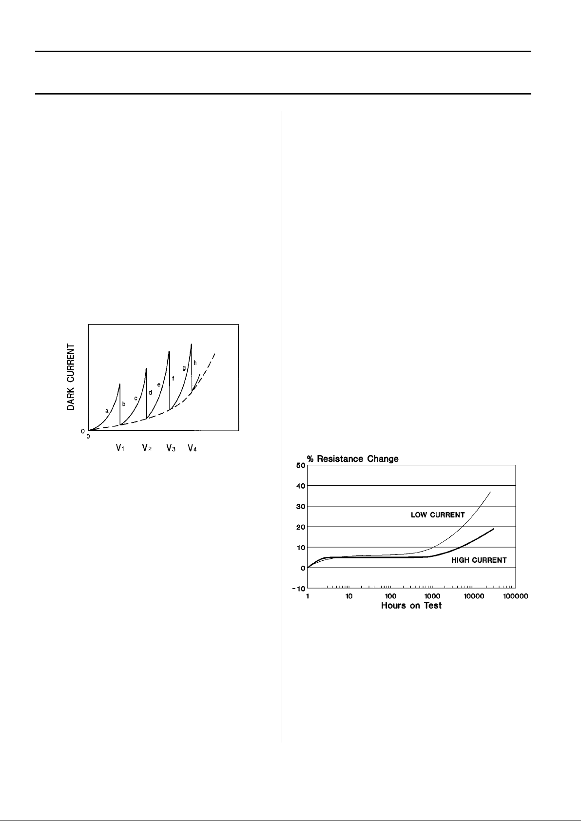
The maximum voltage rating of the output element (photocell) applies
only when the input is off. Two different kinds of dark current “leakage”
characteristics are observed in photocell output elements. Figure 4
shows the soft breakdown found in lower resistivity materials. With no
input, if the applied voltage is suddenly increased from zero to V
1
, the
current increases along section ‘a’, with the steepness depending on
the rate at which the voltage is increased. If the voltage is now held at
V1, the current decreases along curve ‘b’ and stabilizes at a much
lower value. If the voltage is again increased, the next section of the
curve is traversed with the current dropping along curve ‘d’ in time.
This process can be repeated until the reverse current becomes so
great that the cell burns up. The maximum voltage rating for photocells
with this soft reverse characteristic is based on a safe steady-state
power di ssipation in the OFF condition.
Figure 4. Breakdown characteristics of photocells with low resistivity
photoconductive material.
Higher resistivity photoconductive materials do not show the reverse
characteristics of Figure 4 to any significant degree. As voltage is
increased, the dark current increases, but remains very low until
breakdown occurs. The curre nt then increases in an avalanche fashion
resulting in an arc-over which causes the cell to be permanently
damaged (shorted). The dielectric breakdown voltage is approximately
8 - 10 kV per cm of contact spacing for materials with this type of
reverse characteristic. Photocells have 0.16 - 0.5 mm electrode
spacing so the maximum voltage r atings typically fall into the 100 - 300
volt range.
The high voltage capability of photocells suggests their use as the
series pass element in a hig h voltage regulated power sup ply. Voltages
up to 5 or 10 kV can be re gulated but the current should be limited t o 1
or 2 mA. The iso lated input element gr eatly simplifi es the circuit design
and the single output element avoids the need for voltage and current
sharing components.
Power Rating
Photocells are primarily used for signal control since the maximum
allowable power dissipation is low. Typically, the steady-state output
current should be kept below 10 mA on catalog LED AO Is because of
the small size ceramic used in the output cell. However, the surface
area is large compared to similarly r ated transistors, so AOIs with sta nd
signifi cant transient current and power surges.
Power ratings are given in the catalog and are typically a few hundred
milliwatts, but special AOIs have been made with power dissipation
ratings as high as 2.0 W.
Life and Aging
Life expectancy of an AOI is influenced both by the input and output
devices. Isolators which use an LED have long life since LED lifetimes
are long: 10,000 to 200, 000 hours, dep ending on the application. LEDs
normally show a decrease in light output for a specified bias curr ent as
they age.
The photocell output elements in AOIs show an increase in output
resistance o ver time as they age. With a cont inuous input drive curren t
and with voltage bias applied to the output, the output resistance will
generally increase at a rate of 10 percent per year. The aging rate is
lower with intermittent operation. Figure 5 shows the trend line for
output resistance under typical operating conditions. Other AOIs using
different photoconductiv e m aterials show similar trends.
Figure 5. VTL5C3 Life Test.
Page 43

38
Characteristics of Analog Optical Isolators
Storage Characteris t ics
The instantaneous output resistance of any AOI is somewhat
dependent on the short term light history of the photocell output
element. With no applied input current or voltage, th e output element is
in the dark. Dark storage causes the cell to “dark adapt”, a condition
which results in an increase in the photocell’s sensitivity to light. When
first turned on, an AOI which has experienced a period of dark
adaption w ill exhibit a lower value for “on” resistance , at any giv en drive
condition, than the same device which has been continuously on.
The output resistance of an AOI which has been biased “on” is
considered to be constant with time (neglecting long term aging
effects). After the removal of the input drive, the photocell begins to
experience dark adaption. The cell’s rate of increase in sensitivity is
initially high but eventually levels off with time in an exponential
manner. Most of the dark adapt occurs in the first eight hours, but with
some AOIs for sensitivity can continue to increase for several weeks.
When an AOI which has been sitting in the dark is turned on, the cell
immediately begins returning to its light adapted state. For any given
device, the rate of recovery is dependent on the input light level.
The type of photoconductive material is the major factor determining
the magnitude of these changes. Lower resistivity materials show
greater initial and final changes but their rate of chan ge is faster.
These light/dark history effects are pronounced at both high and low
input levels. However, at high input levels, the photocell light adapts
quite rapi dly, usually in minutes .
Figure 1 shows the transfer curves for an AOI after 24 hour storage
with no in put and then after it has been operated wi th rated input for 24
hours. Because of these “memory” phenomena, it is best to use these
parts in a closed loop circuit to minimize the effects of these changes.
Open loop proportional operation is possible if the application can
tolerate variations. The use of the VTL5C2 and VTL5C3 with their
more stable char acteristics will help.
Temperature Range
Operating and storage tem per ature range is l imited at the low er end by
the reduction of dark resistance of the cell and at the upper end by
rapid aging. At low temperatures, the response time of the output cell
increases. The temperature at which this becomes pronounced
depends on the photoconductive material type. Isolators using low
resistivity materials, as in the VTL5C4, will show this lengthening of
response time at -25°C. Higher resistivity material s such as used in t he
VTL5C3 and VTL5C6 do not slow down e xcessively until temperatures
get below -40°C. This characteristic is completely reversible with the
response time recovering when the te mperature rises.
Storage a t l ow temperature has no operating effect on AO Is. Units may
be stored at temperatures as low as -40°C. Lower temperatures may
cause mechanical stress damage in the package which can cause
permanent changes in the A OI transfer cha r acteristics.
The chemistry of the photoconductive materials dictates a maximum
operating and storage temperature of 75°C. It should be noted that
operation of the photocell above 75°C does not usually lead to
catastrophic failure but the photoconductive surface may be damaged,
leading to irr eversible changes in sensitivity.
The amount of resistance change is a function of time as well as
temperature. While changes of several hundred percent will occur in a
matter of a few minutes at 150°C, it will take years at 50°C to produce
that much change.
In most applications, operation is intermittent. At elevated
temperatures, the resistance of the cell rises during the turn-on period
and recovers during the turn-off period, usually resulting in little net
change. However, if the AOI is stored at elevated temperatures for
many hours with no input signal, there is a net reduction in output
resistance. There will be some recovery during operation over time but
it is not possible to predict the rate or to what degree. Elevated
temperatures do not produce sudden catastrophic failure, but changes
in the device transfer curve with time must be anticipated.
Page 44

39
Characteristics of Analog Optical Isolators
Capacitance
The equivalent circuit for the output photocell is a resistor in parallel
with the capacitance. The capacitance arises from the topside
metallization of the electrodes which form a coplanar capacitor. The
value of this capacitance is largely determined by the size of the
ceramic base. For lower capacitance, a smaller cell is needed. The
capacitance is so small (3.0 pF, typical on catalog AOIs) that it is
negligible in most applications. However, there are applications such
as wideband or high frequency amplifiers in which the capacitance
needs to be considered. At 4.5 MHz, the video baseband frequency,
the photocell capacitive reactance is only 12 kilohms. If the phase shift
of the signal is to be kept below 10°, the highest useful cell resistance
is only 2.0 kilohms. At high AOI input drive, where the cell is drive
below 1.0 kilohm, the capacitance can increase additionally from 2 to
10 times, possibly due to distributed effects.
Summary
Analog Optical Isolators have many unique features, such as:
1. High input-t o-output isolatio n.
2. True resistance element output.
3. Wide dynamic range (low “on” resistanc e/h igh “off” resistance).
4. Low drive current.
5. Low distortion.
These features are primarily dependent on which input element and
output element photoconductive material is used in the Vactrol AOI.
Thus, there is a wide variety of Vactrols to choose from for your
application.
Page 45
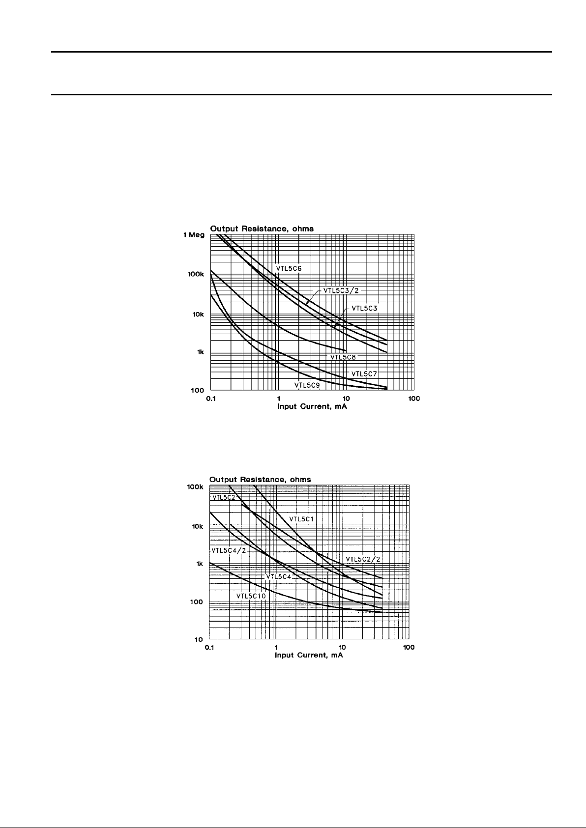
40
Characteristics of Analog Optical Isolators
Typical Transfer Characteristi cs (Resista nce vs. Input C urrent) For Standard Vactrols
Curves shown are based upon a light adapt condition for 24 hours @ no input at 25°C.
Output Resistance v s. Input Current
VTL5C Series
Output Resistance v s. Input Current
VTL5C Series
Page 46
41
Characteristics of Analog Optical Isolators
Analog Optoisolator Comparison Chart
Specifica t ion Note s
(These notes are referenced on the following LED Vactrol Data Sheet pages.)
Since the input has a substant ially constant voltage drop, a curre nt limiting resistance is required.
Dark adapted resistance mea sured after 24 or more hours of no input.
Measured 10 sec. after removal of the input. The ultimate resistance is many times greater than the value at 10 seconds.
Ascent measured to 63% of final conductance from the application of 40 mA input. The conductance rise time to a specified value is
increased at red uced input dri ve while the conductance de cay time to a specified v alue is de creased.
Typical matching and t racking from 0.4 to 40 m A is 25%.
Measured 5 sec. after removal of the input. The ultimate resistance is many times greater than the value at 5 seconds.
VTL5C9 response tim es are based on a 2.0 mA input. VTL5C10 response times are based on a 10.0 mA input for as cent time an d
a 1.0 mA input for decay t i m e.
Device Material Type Slope D ynam ic Range Dark Resistance
Temperature
Coefficient
Speed of
Response
Light History
Effect
VTL5C1 1 15.0 100 db 50 MΩ Very High Very Fast Very Large
VTL5C2 Ø 24.0 69 db 1 MΩ Low Slow Small
VTL5C2/2 Ø 20.0 65 db 1 MΩ Low Slow Small
VTL5C3 3 20.0 75 db 10 MΩ Very Low Very Slow Very Small
VTL5C3/2 3 19.0 71 db 10 MΩ Very Low Very Slow Very Small
VTL5C4 4 18.7 72 db 400 MΩ High Fast Large
VTL5C4/2 4 8.3 68 db 400 MΩ High Fast Large
VTL5C6 Ø 16.7 88 db 100 MΩ Low Slow Small
VTL5C7 7 5.7 75 db 1 MΩ Average Average Average
VTL5C8 Ø 8.0 80 db 1 0 MΩ Low Slow S mall
VTL5C9 1 7.3 112 db 50 MΩ Very High Very Fast Very Large
VTL5C10 4 3.8 75 db 400 MΩ High Fast Large
1
2
3
4
5
6
7
Page 47

42
Page 48
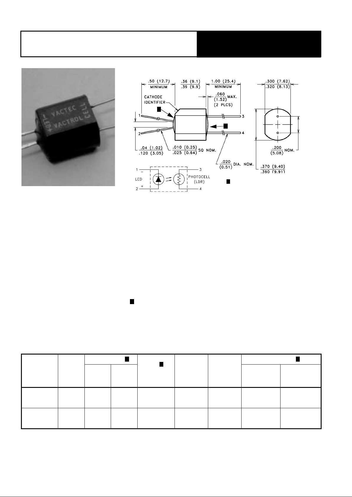
43
Low Cost Axial Vactrols VTL5C1, 5C2
PACKAGE DIMENSIONS inch (mm)
PLASTIC POTTING CONTOUR
NOT CONTROLLED
DESCRIPTION
VTL5C1 offers 100db dynamic range, fas t response time, and very high dark resistance.
VTL5C2 features a very steep slope, low temperature coefficient of resistance, and a small light history memory.
ABSOLUTE MAXIMUM RATINGS @ 25°C
Maximum Temperatures
Storage and Operating: –40°C to 75°C
Cell Power: 175 mW
Derate abo ve 30°C: 3.9 mW/°C
LED Current: 40 mA
Derate abo ve 30°C: 0.9 mA/°C
LED Reverse Breakdown Voltage: 3.0 V
1
LED Forward Voltage Drop @ 20 mA: 2.0V (1.65V Typ.)
Min. Isolation Voltage @ 70% Rel. Humidity: 25 00 VR MS
Output Cell Capacitance: 5.0 pF
Cell Voltage: 100V (VT L5C 1),
200V (VTL5C2)
Input - Output Coupling Capacitance: 0.5 pF
ELECTRO-OPTICAL CHARCTERISTICS @ 25°C
Refer to Specification Notes, page 41.
Part
Number
Material
Type
ON Resistance
OFF
Resistance
@ 10 sec. (Min.)
Slope
(Typ.)
Dynamic Range
(Typ.)
Response Time
Input current
Dark
Adapted
(Typ.)
Turn-on to
63% Final R
ON
(Typ.)
Turn-off (Decay)
to 100 kΩ
(Max.)
VTL5C1 1
1 mA
10 mA
40 mA
20 kΩ
600 Ω
200 Ω
50 MΩ 15 100 db 2.5 ms 35 ms
VTL5C2 0
1 mA
10 mA
40 mA
5.5 kΩ
800 Ω
200 Ω
1 MΩ 24 69 db 3.5 ms 500 ms
2
3
@ 0.5 mA
R@ 5 mA
------------------------
R
DARK
R@ 20 mA
----------------------- -
4
PerkinElmer Optoelectronics, 10900 Page Ave., St. Louis, MO 63132 USA Phone: 314-423-4900 Fax: 314-423-3956 Web: www.perkinelmer.com/opto
Page 49
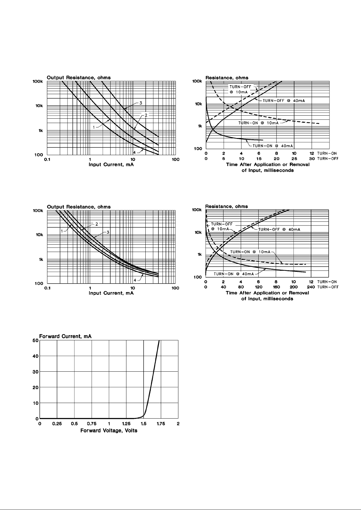
44
Typical Performance Curves
Output Resistance vs. Input Current
VTL5C1
Output Resistance vs. Input Current
VTL5C2
Input Characteristics
Response Time
VTL5C1
Response Time
VTL5C2
Notes:
1. At 1.0 mA and belo w, units may have substanti ally higher
resistance than shown in the typical curves . C onsult factory if
closely controll ed characteristics are requi red at low input
currents.
2. Output resistance vs input current transfer curves are given for
the foll owing light adapt cond it ions:
(1) 25°C — 24 hours @ no input
(2) 25°C — 24 hours @ 40 mA input
(3) +50°C — 24 hours @ 40 mA input
(4) –20°C — 24 hours @ 40 mA input
3. Response time characteristics are based upon te st following
adapt condition (2) above.
PerkinElmer Optoelectronics, 10900 Page Ave., St. Louis, MO 63132 USA Phone: 314-423-4900 Fax: 314-423-3956 Web: www.perkinelmer.com/opto
Page 50
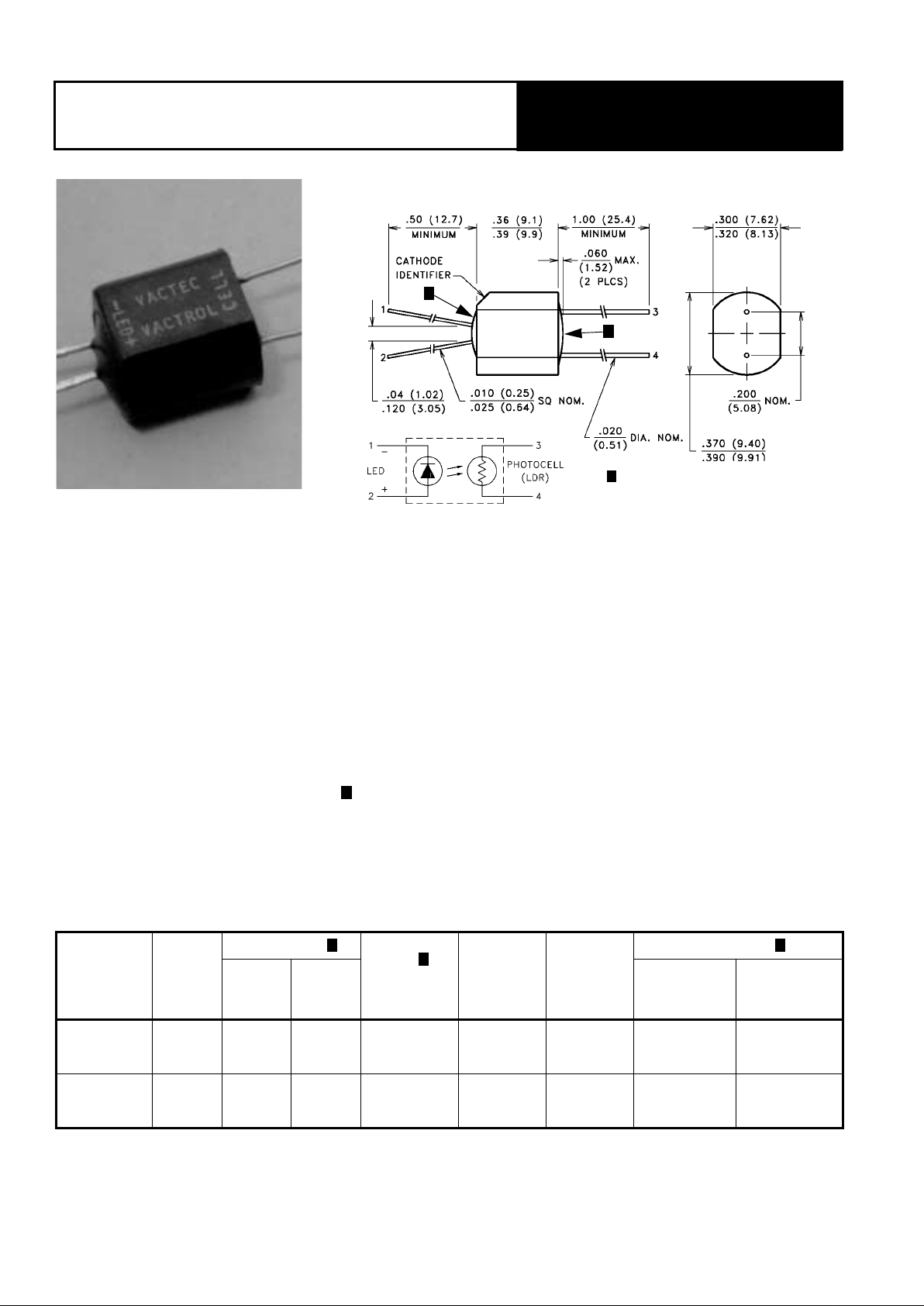
45
Low Cost Axial Vactrols VTL5C3, 5C4
PACKAGE DIMENSIONS INCH (MM)
PLASTIC POTTING CONTOUR
NOT CONTROLLED
DESCRIPTION
VTL5C 3 has a st ee p s lope, go od dyna mic r ang e, a ver y l ow t empe rat ure coe ffic ien t of r esist anc e, a nd a sma ll li ght hi stor y mem or y.
VTL5C4 features a very low “on” resistance, fast response time, with a smaller temperature coefficient of resistance than VTL5C1.
ABSOLUTE MAXIMUM RATINGS @ 25°C
Maximum Temperatures
Storage and Operating: –40°C to 75°C
Cell Power: 175 mW
Derate abo ve 30°C: 3.9 mW/°C
LED Current: 40 mA
Derate abo ve 30°C: 0.9 mA/°C
LED Reverse Breakdown Voltage: 3.0 V
1
LED Forward Voltage Drop @ 20 mA: 2.0V (1.65V Typ.)
Min. Isolation Voltage @ 70% Rel. Humidity: 25 00 VR MS
Output Cell Capacitance: 5.0 pF
Cell Voltage: 250V (VT L5C 3),
50V (VTL5C 4)
Input - Output Coupling Capacitance: 0.5 pF
ELECTRO-OPTICAL CHARCTERISTICS @ 25°C
Refer to Specification Notes, page 41.
Part
Number
Material
Type
ON Resistance
OFF
Resistance
@ 10 sec. (Min.)
Slope
(Typ.)
Dynamic Range
(Typ.)
Response Time
Input current
Dark
Adapted
(Typ.)
Turn-on to
63% Final R
ON
(Typ.)
Turn-off (Decay)
to 100 kΩ
(Max.)
VTL5C3 3
1 mA
10 mA
40 mA
30 kΩ
5 Ω
1.5 Ω
10 MΩ 20 75 db 2.5 ms 35 ms
VTL5C4 4
1 mA
10 mA
40 mA
1.2 kΩ
125 Ω
75 Ω
400 MΩ 18.7 72 db 6.0 ms 1.5 sec
2
3
R@ 0.5 mA
R@ 5 mA
-------------------------
R
DARK
R@ 20 mA
----------------------- -
4
PerkinElmer Optoelectronics, 10900 Page Ave., St. Louis, MO 63132 USA Phone: 314-423-4900 Fax: 314-423-3956 Web: www.perkinelmer.com/opto
Page 51
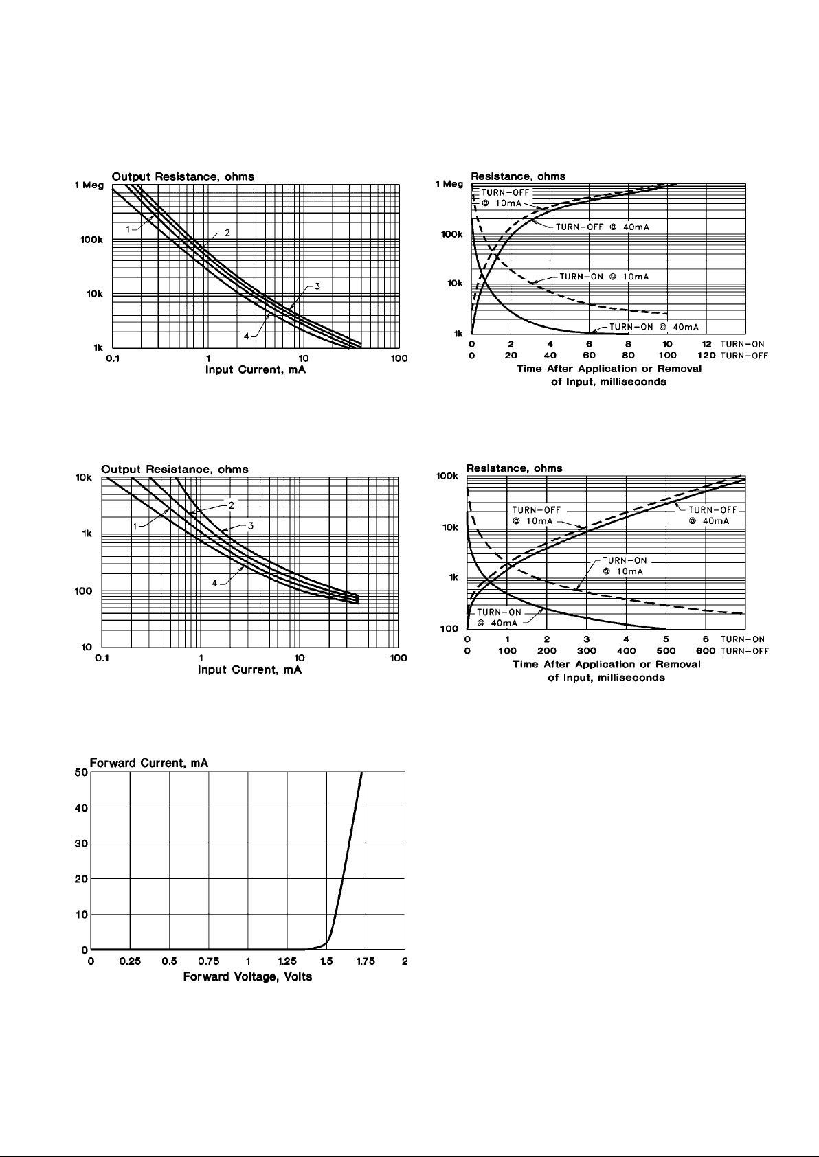
46
Typical Performance Curves
Output Resistance vs. Input Current
VTL5C3
Output Resistance vs. Input Current
VTL5C4
Input Characteristics
Response Time
VTL5C3
Response Time
VTL5C4
Notes:
1. At 1.0 mA and belo w, units may have substanti ally higher
resistance than shown in the typical curves . C onsult factory if
closely controll ed characteristics are requi red at low input
currents.
2. Output resistance vs input current transfer curves are given for
the foll owing light adapt cond it ions:
(1) 25°C — 24 hours @ no input
(2) 25°C — 24 hours @ 40 mA input
(3) +50°C — 24 hours @ 40 mA input
(4) –20°C — 24 hours @ 40 mA input
3. Response time characteristics are based upon te st following
adapt condition (2) above.
PerkinElmer Optoelectronics, 10900 Page Ave., St. Louis, MO 63132 USA Phone: 314-423-4900 Fax: 314-423-3956 Web: www.perkinelmer.com/opto
Page 52
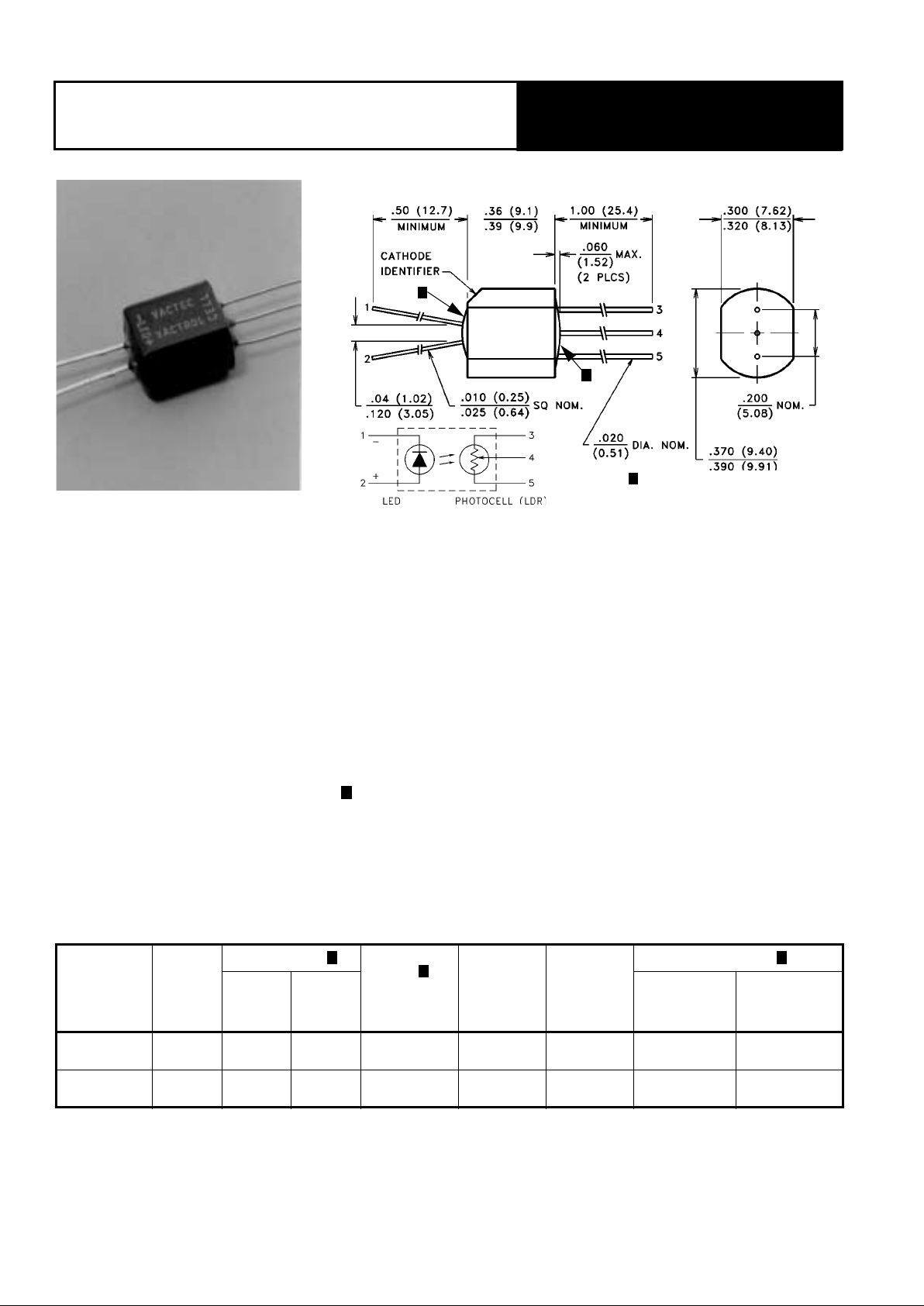
47
Dual Element Axial Vactrols VTL5C2/2, 5C3/2
PACKAGE DIMENSIONS INCH (MM)
PLASTIC POTTING CONTOUR
NOT CONTROLLED
DESCRIPTION
VTL5C2/2 features a very steep slope, low temperature coefficient of resista nce, and a small light history memory.
VTL5C3/2 has a steep slope, good dynamic range, a very low temperat ur e coefficient of resistance, and a small light history memory.
ABSOLUTE MAXIMUM RATINGS @ 25°C
Maximum Temperatures
Storage and Operating: –40°C to 75°C
Cell Power: 175 mW
Derate abo ve 30°C: 3.9 mW/°C
LED Current: 40 mA
Derate abo ve 30°C: 0.9 mA/°C
LED Reverse Breakdown Voltage: 3.0 V
1
LED Forward Voltage Drop @ 20 mA: 2.0V (1.65V Typ.)
Min. Isolation Voltage @ 70% Rel. Humidity: 25 00 VR MS
Output Cell Capacitance: 5.0 pF
Cell Voltage: 50V (VTL5C2/2),
100V (VTL5C2/3)
Input - Output Coupling Capacitance: 0.5 pF
ELECTRO-OPTICAL CHARCTERISTICS @ 25°C
Refer to Specification Notes, page 41.
Part
Number
Material
Type
ON Resistance
OFF
Resistance
@ 10 sec. (Min.)
Slope
(Typ.)
Dynamic Range
(Typ.)
Response Time
Input current
Dark
Adapted
(Typ.)
Turn-on to
63% Final R
ON
(Typ.)
Turn-off (Decay)
to 100 kΩ
(Max.)
VTL5C2/2 Ø
5 mA
40 mA
2.5 kΩ
700 Ω
1.0 MΩ 20 65 db 7.0 ms 150 ms
VTL5C3/2 3
1 mA
40 mA
55 kΩ
2 Ω
10 MΩ 19 71 db 3.0 ms 50 ms
2
3
@ 0.5 mA
R@ 5 mA
------------------------
R
DARK
R@ 20 mA
----------------------- -
4
PerkinElmer Optoelectronics, 10900 Page Ave., St. Louis, MO 63132 USA Phone: 314-423-4900 Fax: 314-423-3956 Web: www.perkinelmer.com/opto
Page 53
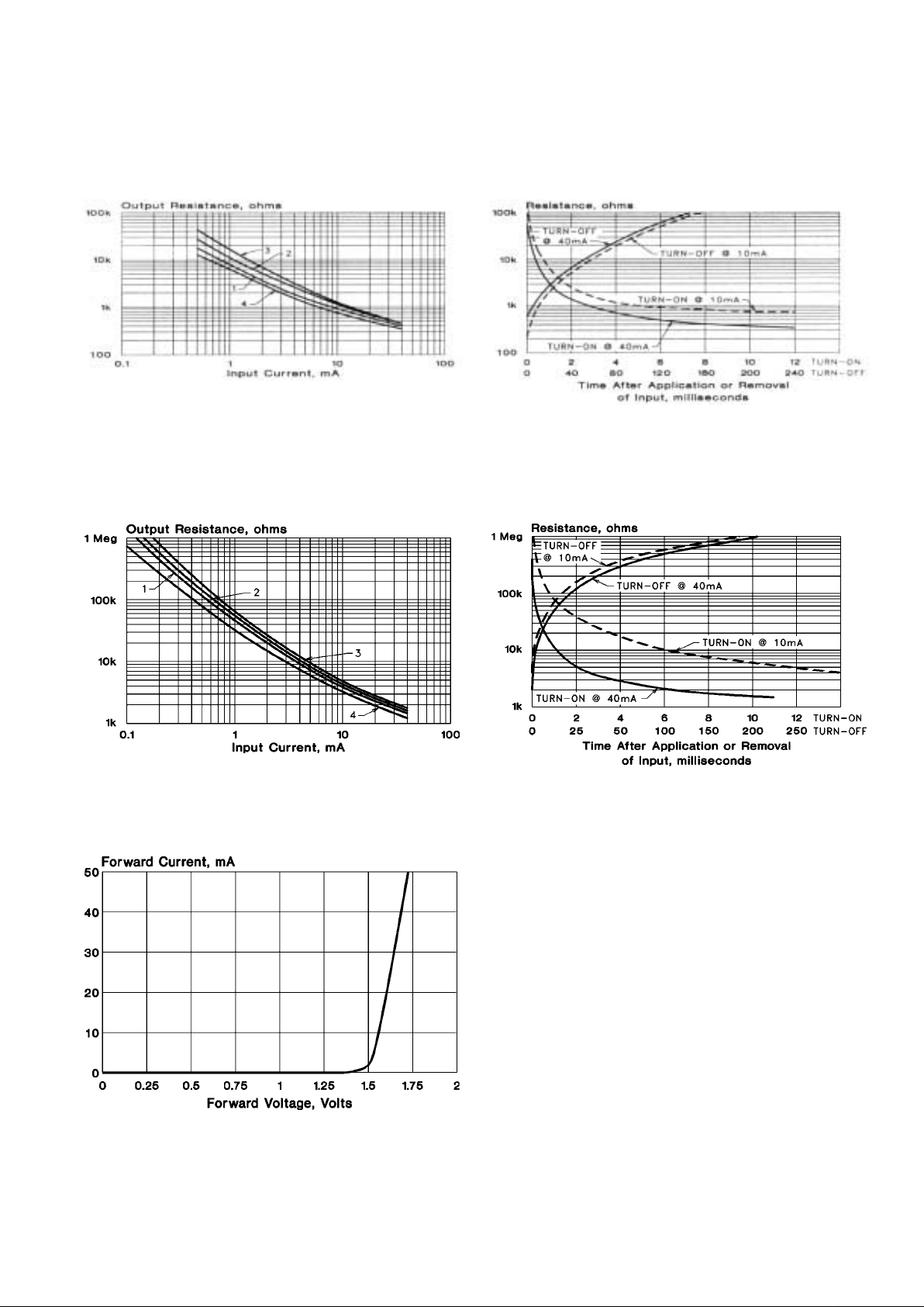
48
Typical Performance Curves
Output Resistance vs. Input Current
VTL5C2/2
Output Resistance vs. Input Current
VTL5C3/2
Input Characteristics
Response Time
VTL5C2/2
Response Time
VTL5C3/2
Notes:
1. At 1.0 mA and belo w, units may have substanti ally higher
resistance than shown in the typical curves . C onsult factory if
closely controll ed characteristics are requi red at low input
currents.
2. Output resistance vs input current transfer curves are given for
the foll owing light adapt cond it ions:
(1) 25°C — 24 hours @ no input
(2) 25°C — 24 hours @ 40 mA input
(3) +50°C — 24 hours @ 40 mA input
(4) –20°C — 24 hours @ 40 mA input
3. Response time characteristics are based upon te st following
adapt condition (2) above.
PerkinElmer Optoelectronics, 10900 Page Ave., St. Louis, MO 63132 USA Phone: 314-423-4900 Fax: 314-423-3956 Web: www.perkinelmer.com/opto
Page 54
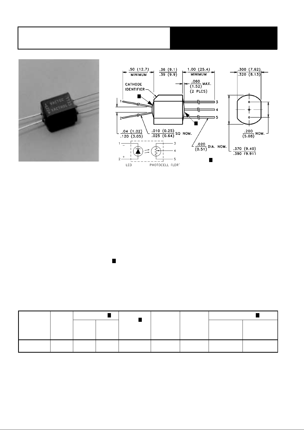
49
Dual Element Axial Vactrols VTL5C4/2
PACKAGE DIMENSIONS INCH (MM)
PLASTIC POTTING CONTOUR
NOT CONTROLLED
DESCRIPTION
VTL5C4/2 features a very low “on” resistance, fast response time, with a smaller temperature coefficient of resistance than VTL5C1.
ABSOLUTE MAXIMUM RATINGS @ 25°C
Maximum Temperatures
Storage and Operating: –40°C to 75°C
Cell Power: 175 mW
Derate abo ve 30°C: 3.9 mW/°C
LED Current: 40 mA
Derate abo ve 30°C: 0.9 mA/°C
LED Reverse Breakdown Voltage: 3.0 V
1
LED Forward Voltage Drop @ 20 mA: 2.0V (1.65V Typ.)
Min. Isolation Voltage @ 70% Rel. Humidity: 25 00 VR MS
Output Cell Capacitance: 5.0 pF
Cell Voltage: 30V
Input - Output Coupling Capacitance: 0.5 pF
ELECTRO-OPTICAL CHARCTERISTICS @ 25°C
Refer to Specification Notes, page 41.
Part
Number
Material
Type
ON Resistance
OFF
Resistance
@ 10 sec. (Min.)
Slope
(Typ.)
Dynamic Range
(Typ.)
Response Time
Input c u rrent
Dark
Adapted
(Typ.)
Turn-on to
63% Final R
ON
(Typ.)
Turn-off (Decay)
to 100 kΩ
(Max.)
VTL5C4/2 4
1 mA
10 mA
1.5 kΩ
150 Ω
400 Ω 8.3 68 db 6.0 ms 1.5 sec
2
3
@ 0.5 mA
R@ 5 mA
------------------------
R
DARK
R@ 20 mA
----------------------- -
4
PerkinElmer Optoelectronics, 10900 Page Ave., St. Louis, MO 63132 USA Phone: 314-423-4900 Fax: 314-423-3956 Web: www.perkinelmer.com/opto
Page 55
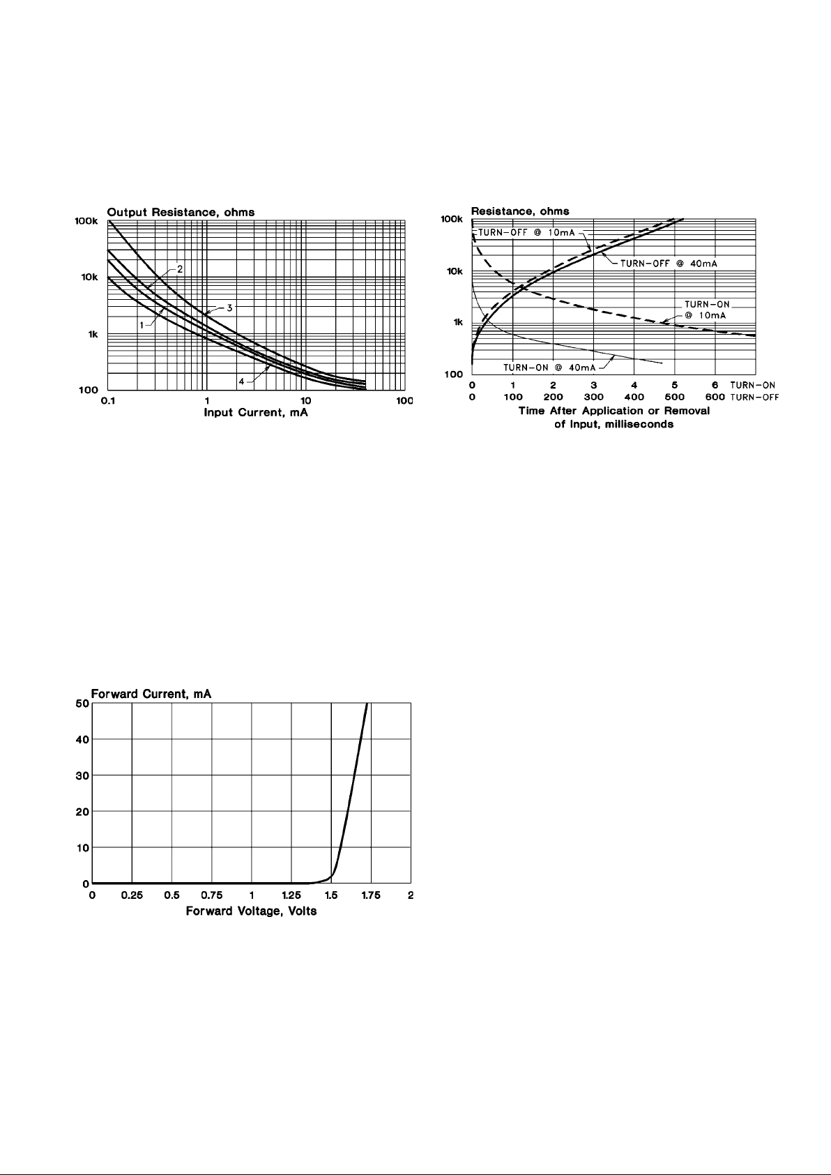
50
Typical Performance Curves (Per Element)
Output Resistance vs. Input Current
VTL5C4/2
Input Characteristics
Response Time
VTL5C4/2
Notes:
1. At 1.0 mA and belo w, units may have substanti ally higher
resistance than shown in the typical curves . C onsult factory if
closely controll ed characteristics are requi red at low input
currents.
2. Output resistance vs input current transfer curves are given for
the foll owing light adapt cond it ions:
(1) 25°C — 24 hours @ no input
(2) 25°C — 24 hours @ 40 mA input
(3) +50°C — 24 hours @ 40 mA input
(4) –20°C — 24 hours @ 40 mA input
3. Response time characteristics are based upon te st following
adapt condition (2) above.
PerkinElmer Optoelectronics, 10900 Page Ave., St. Louis, MO 63132 USA Phone: 314-423-4900 Fax: 314-423-3956 Web: www.perkinelmer.com/opto
Page 56
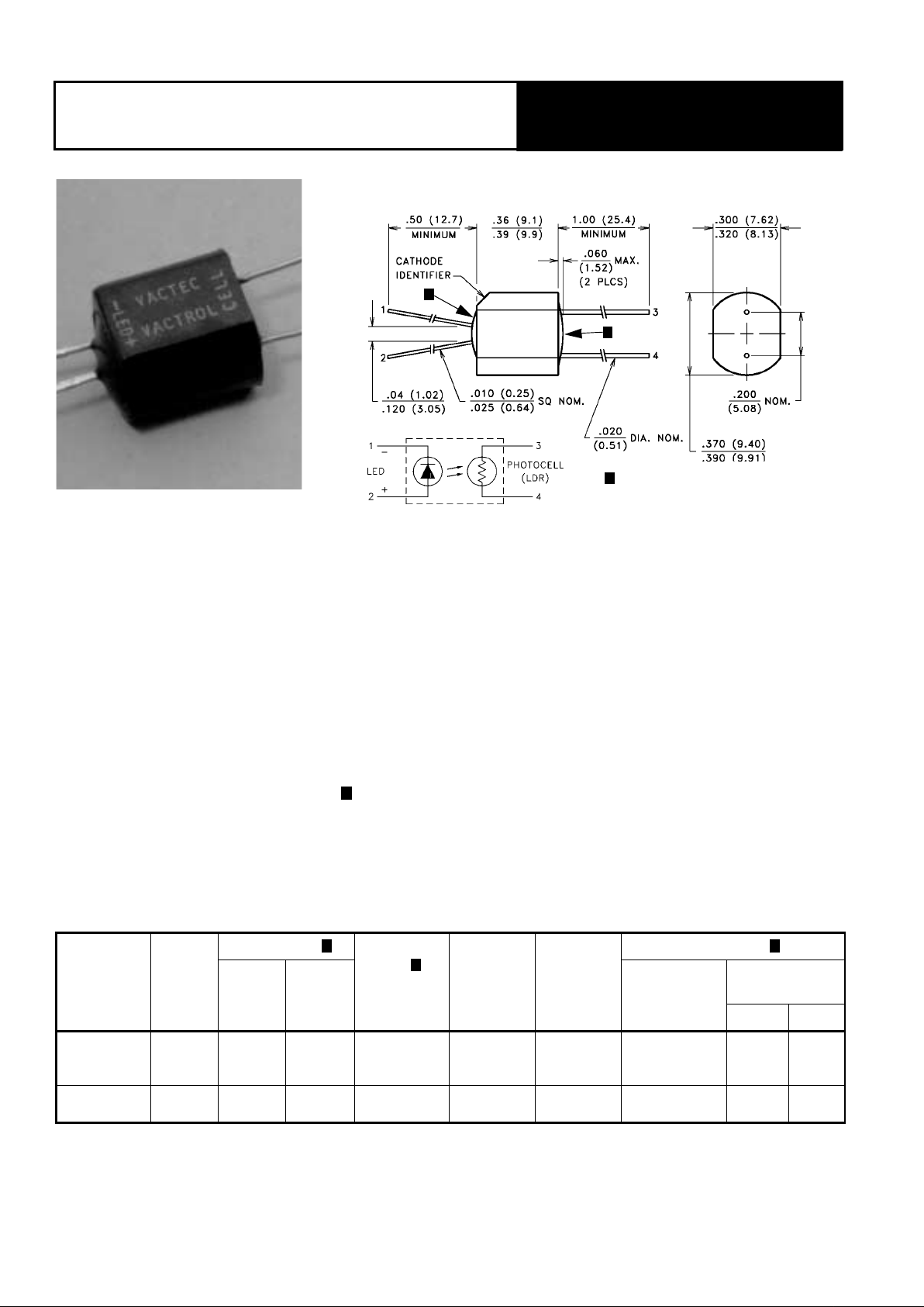
51
Low Cost Axial Vactrols VTL5C6, 5C7
PACKAGE DIMENSIONS INCH (MM)
PLASTIC POTTING CONTOUR
NOT CONTROLLED
DESCRIPTION
VTL5C6 has a large dynamic range, high dark resistance, a low temperature coeffecient of resistance, and a small light history
memory. VTL5C7 is a shallow sloped device with good dynamic range, average temperature coefficient of resistance, speed of
response, and light history memory.
ABSOLUTE MAXIMUM RATINGS @ 25°C
Maximum Temperatures
Storage and Operating: –40°C to 75°C
Cell Power: 175 mW
Derate abo ve 30°C: 3.9 mW/°C
LED Current: 40 mA
Derate abo ve 30°C: 0.9 mA/°C
LED Reverse Breakdown Voltage: 3.0 V
1
LED Forward Voltage Drop @ 20 mA: 2.0V (1.65V Typ.)
Min. Isolation Voltage @ 70% Rel. Humidity: 25 00 VR MS
Output Cell Capacitance: 5.0 pF
Cell Voltage: 250V (VT L5C 6),
50V (VTL5C 7)
Input - Output Coupling Capacitance: 0.5 pF
ELECTRO-OPTICAL CHARCTERISTICS @ 25°C
Refer to Specification Notes, page 41.
Part
Number
Material
Type
ON Resistance
OFF
Resistance
@ 10 sec. (Min.)
Slope
(Typ.)
Dynamic Range
(Typ.)
Response Time
Input
current
Dark
Adapted
(Typ.)
Turn-on to
63% Final R
ON
(Typ.)
Turn-off (Decay)
to (Max .)
1 MΩ 100 kΩ
VTL5C6 0
1 mA
10 mA
40 mA
75 kΩ
10 kΩ
2 kΩ
100 MΩ 16.7 88 db 3.5 ms 50 ms
VTL5C7 7
0.4 mA
2 mA
5 kΩ
1.1 kΩ
1 MΩ 5.7 75 db 6.0 ms 1 sec
2
3
@ 0.5 mA
R@ 5 mA
------------------------
R
DARK
R@ 20 mA
----------------------- -
4
PerkinElmer Optoelectronics, 10900 Page Ave., St. Louis, MO 63132 USA Phone: 314-423-4900 Fax: 314-423-3956 Web: www.perkinelmer.com/opto
Page 57
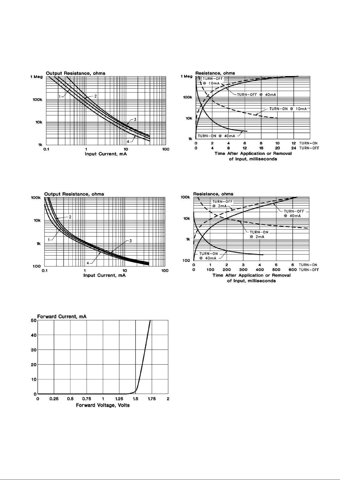
52
Typical Performance Curves
Output Resistance vs. Input Current
VTL5C6
Output Resistance vs. Input Current
VTL5C7
Input Characteristics
Response Time
VTL5C6
Response Time
VTL5C7
Notes:
1. At 1.0 mA and belo w, units may have substanti ally higher
resistance than shown in the typical curves . C onsult factory if
closely controll ed characteristics are requi red at low input
currents.
2. Output resistance vs input current transfer curves are given for
the foll owing light adapt cond it ions:
(1) 25°C — 24 hours @ no input
(2) 25°C — 24 hours @ 40 mA input
(3) +50°C — 24 hours @ 40 mA input
(4) –20°C — 24 hours @ 40 mA input
3. Response time characteristics are based upon te st following
adapt condition (2) above.
PerkinElmer Optoelectronics, 10900 Page Ave., St. Louis, MO 63132 USA Phone: 314-423-4900 Fax: 314-423-3956 Web: www.perkinelmer.com/opto
Page 58
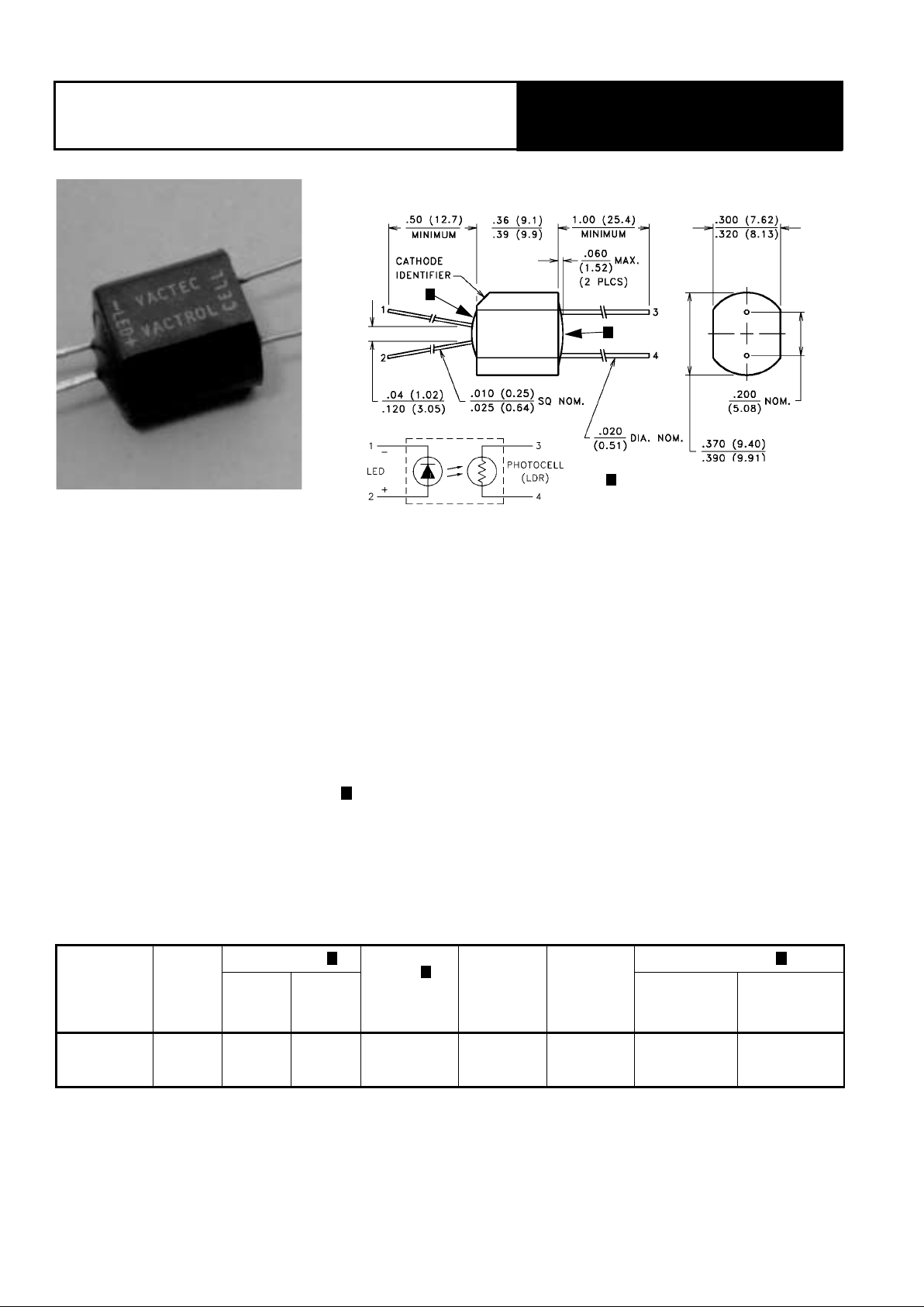
53
Low Cost Axial Vactrols VTL5C8
PACKAGE DIMENSIONS INCH (MM)
PLASTIC POTTING CONTOUR
NOT CONTROLLED
DESCRIPTION
VTL5C8 is similar to VTL5C2 with a low temperature coefficient of resistance and little light history memory, but has a more shallow
slope and a lower “on” resi st ance at lo w (1 mA) drive currents.
ABSOLUTE MAXIMUM RATINGS @ 25°C
Maximum Temperatures
Storage and Operating: –40°C to 75°C
Cell Power: 175 mW
Derate abo ve 30°C: 3.9 mW/°C
LED Current: 40 mA
Derate abo ve 30°C: 0.9 mA/°C
LED Reverse Breakdown Voltage: 3.0 V
1
LED Forward Voltage Drop @ 20 mA: 2.8V (2.2V Typ.)
Min. Isolation Voltage @ 70% Rel. Humidity: 25 00 VR MS
Output Cell Capacitance: 5.0 pF
Cell Voltage: 500V
Input - Output Coupling Capacitance: 0.5 pF
ELECTRO-OPTICAL CHARCTERISTICS @ 25°C
Refer to Specification Notes, page 41.
Part
Number
Material
Type
ON Resistance
OFF
Resistance
@ 10 sec. (Min.)
Slope
(Typ.)
Dynamic Range
(Typ.)
Response Time
Input c u rrent
Dark
Adapted
(Typ.)
Turn-on to
63% Final R
ON
(Typ.)
Turn-off (Decay)
to 100 kΩ
(Max.)
VTL5C8 0
1 mA
4 mA
16 mA
4.8 kΩ
1.8 kΩ
1.0 kΩ
10 MΩ 8 80 db 4 ms 60 ms
2
3
@ 0.5 mA
R@ 5 mA
------------------------
R
DARK
R@ 20 mA
----------------------- -
4
PerkinElmer Optoelectronics, 10900 Page Ave., St. Louis, MO 63132 USA Phone: 314-423-4900 Fax: 314-423-3956 Web: www.perkinelmer.com/opto
Page 59
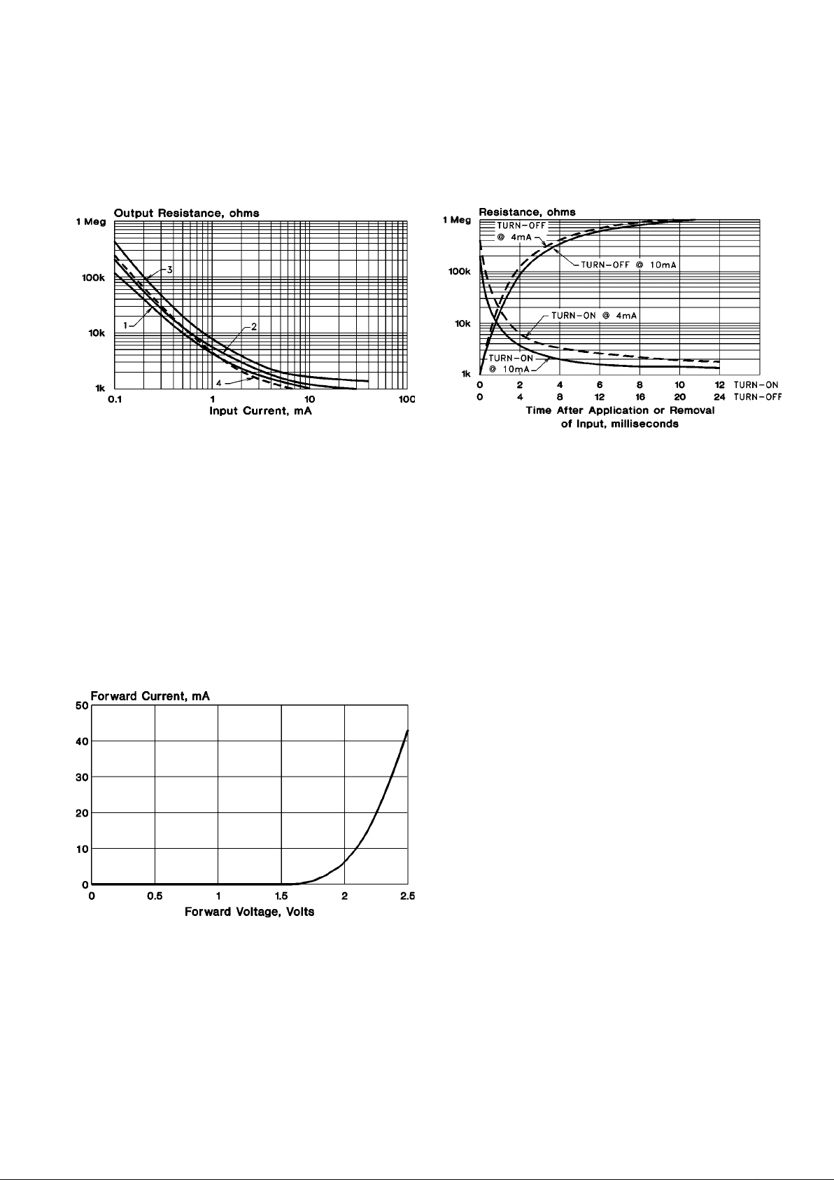
54
Typical Performance Curves
Output Resistance vs. Input Current
VTL5C8
Input Characteristics
Response Time
VTL5C8
Notes:
1. At 1.0 mA and belo w, units may have substanti ally higher
resistance than shown in the typical curves . C onsult factory if
closely controll ed characteristics are requi red at low input
currents.
2. Output resistance vs input current transfer curves are given for
the foll owing light adapt cond it ions:
(1) 25°C — 24 hours @ no input
(2) 25°C — 24 hours @ 40 mA input
(3) +50°C — 24 hours @ 40 mA input
(4) –20°C — 24 hours @ 40 mA input
3. Response time characteristics are based upon te st following
adapt condition (2) above.
PerkinElmer Optoelectronics, 10900 Page Ave., St. Louis, MO 63132 USA Phone: 314-423-4900 Fax: 314-423-3956 Web: www.perkinelmer.com/opto
Page 60
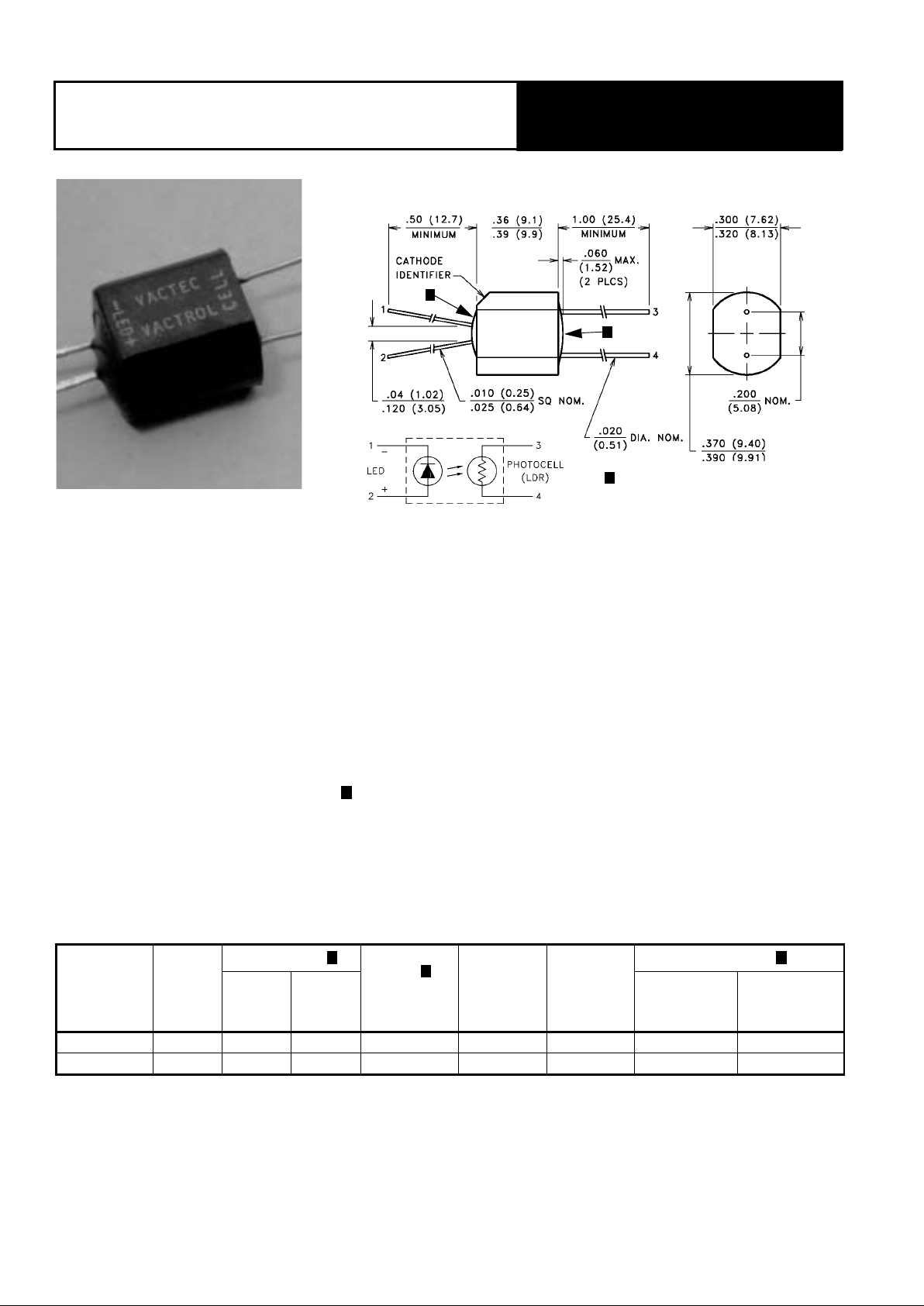
55
Low Cost Axial Vactrols VTL5C9, 5C10
PACKAGE DIMENSIONS INCH (MM)
PLASTIC POTTING CONTOUR
NOT CONTROLLED
DESCRIPTION
VTL5C9 has a 112 db dynamic range, fast response time, high dark resistance, but with a more shallow slope and lower “on”
resis tance at low (1 mA) dr ive cu rrents than the VTL5C1. VTL510 offers a low “ on” re sistan ce at low dr ive cur rents, a fast res ponse
time, an d has a smaller t em perature coefficient t ha n t he VTL5C9.
ABSOLUTE MAXIMUM RATINGS @ 25°C
Maximum Temperatures
Storage and Operating: –40°C to 75°C
Cell Power: 175 mW
Derate abo ve 30°C: 3.9 mW/°C
LED Current: 40 mA
Derate abo ve 30°C: 0.9 mA/°C
LED Reverse Breakdown Voltage: 3.0 V
1
LED Forward Voltage Drop @ 20 mA: 2.8V (2.2V Typ.)
Min. Isolation Voltage @ 70% Rel. Humidity: 25 00 VR MS
Output Cell Capacitance: 5.0 pF
Cell Voltage: 100V (VT L5C 9),
50V (VTL5C 10)
Input - Output Coupling Capacitance: 0.5 pF
ELECTRO-OPTICAL CHARCTERISTICS @ 25°C
Refer to Specification Notes, page 41.
Part
Number
Material
Type
ON Resistance
OFF
Resistance
@ 10 sec. (Min.)
Slope
(Typ.)
Dynamic Range
(Typ.)
Response Time
Input c u rrent
Dark
Adapted
(Typ.)
Turn-on to
63% Final R
ON
(Typ.)
Turn-off (Decay)
to 100 kΩ
(Max.)
VTL5C9 1 2 mA 630 Ω 50 MΩ 7.3 112 db 4.0 ms 50 ms
VTL5C10 4 2 mA 400 Ω 400 K Ω 3.8 75 db 1.0 ms 1.5 sec
2
3
@ 0.5 mA
R@ 5 mA
------------------------
R
DARK
R@ 20 mA
----------------------- -
4
PerkinElmer Optoelectronics, 10900 Page Ave., St. Louis, MO 63132 USA Phone: 314-423-4900 Fax: 314-423-3956 Web: www.perkinelmer.com/opto
Page 61
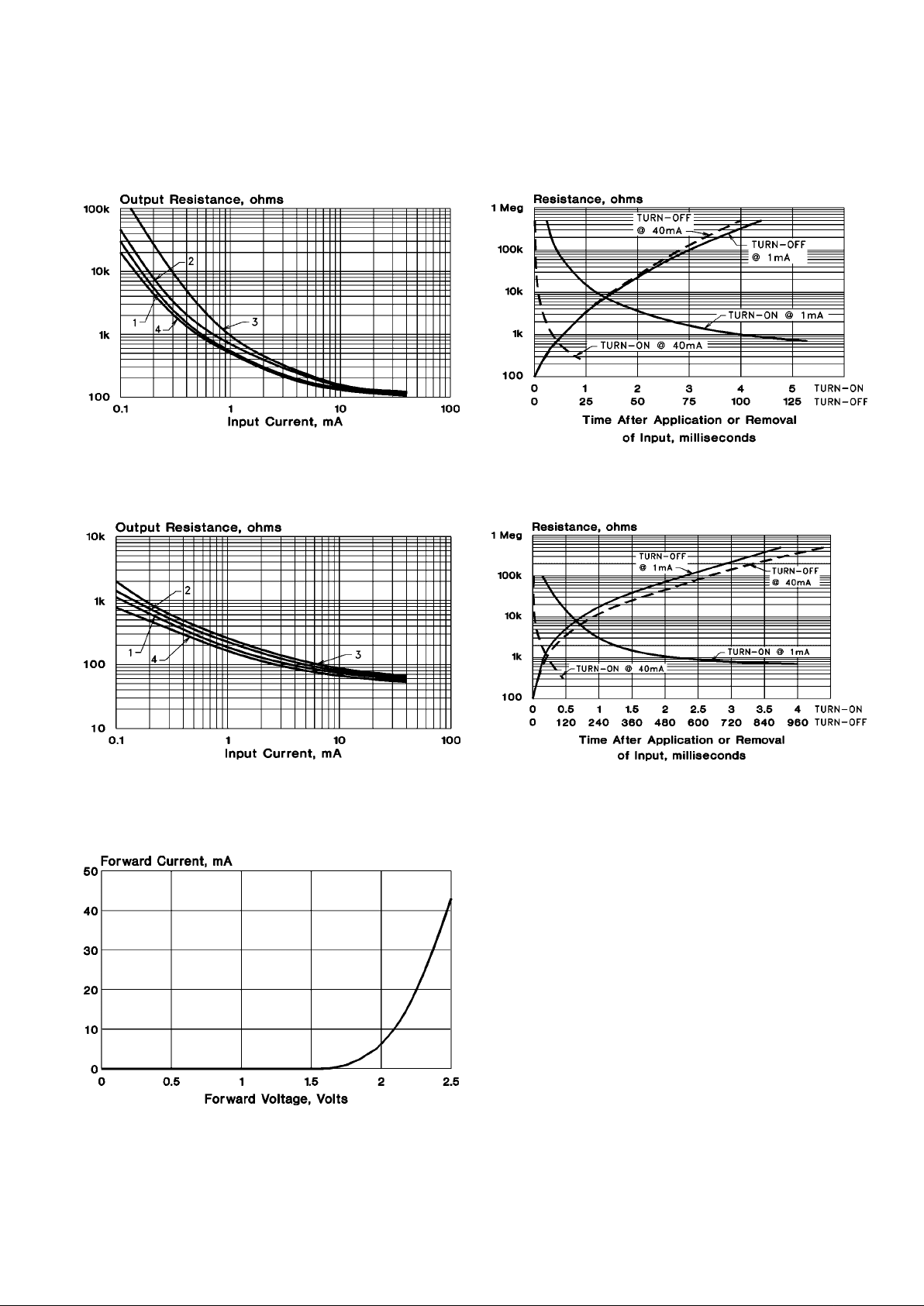
56
Typical Performance Curves
Output Resistance vs. Input Current
VTL5C9
Output Resistance vs. Input Current
VTL5C10
Input Characteristics
Response Time
VTL5C9
Response Time
VTL5C10
Notes:
1. At 1.0 mA and belo w, units may have substanti ally higher
resistance than shown in the typical curves . C onsult factory if
closely controll ed characteristics are requi red at low input
currents.
2. Output resistance vs input current transfer curves are given for
the foll owing light adapt cond it ions:
(1) 25°C — 24 hours @ no input
(2) 25°C — 24 hours @ 40 mA input
(3) +50°C — 24 hours @ 40 mA input
(4) –20°C — 24 hours @ 40 mA input
3. Response time characteristics are based upon te st following
adapt condition (2) above.
PerkinElmer Optoelectronics, 10 900 Page Ave., S t. Louis, MO 63132 USA Phone: 314-423-4900 Fax: 314-423-3956 Web: www.perkinelmer.com/opto
Page 62

57
Application Notes—Analog Optical Isolators
APPLICATION NOTE #1 Audio Applications
The LDR output element of AOIs is almost purely resistive in nature.
This property makes the AOI a very useful device for the control of AC
signals. Further, because AOIs also possess very low noise and low
harmonic distortion characteristics, they are ideal for use as variable
resistors, capable of being remotely adjusted in a wide range of audio
applications and control circuits.
The focus of this note is on the use of AOIs in audio applications.
However, many of the approaches used are equally applicable to
higher frequency AC amplifi cation and control circuits.
Control Circuits
Voltage Divid e r Ci rcuits
The output element of the AOI is a two terminal variable resistor and
may be used in a volta ge divider circuit as shown in Figures 1a and 1b.
Shunt Input Control
Figure 1a shows the AOI as the shunt element. With IF = 0, the
photocell has a very high resistance so e
out
= ein. When IF is inje cte d
into the LED, the AOI output resistance decreases pulling down the
output voltage. Since the cell cannot be driven to zero resistance, the
value of R1 must be selected to give the desired maximum attenuation.
A VTL5C4 with a maximum “on” resistance of 200 ohms at I
F
= 10 mA
requires an R1 of 6100 ohms for 30 db voltage attenuation (producing
a 1000:1 po w er ratio). The actua l at te nuation ratio will be greater since
the 10 mA “on” resis tance is typically 125 ohms .
When the maximum I
F
is less than 10 mA, the series resistance must
be greater to get the same attenuation ratio. If R1 is made large, the
insertion loss (db atten uation at IF = 0) wi ll be higher when the output is
loaded. The maximum voltage across the photocell in this circuit is
equal to the input voltage assuming no insertion loss. An input voltage
as high as 5 – 10V will produce noticeable distortion but that will drop
as I
F
is increased. To minimize distortion, the voltage across the cell
should be ke pt below 1.0V at the normal operat ing point.
Series Input Control
With an AOI as the series element as shown in Figure 1b, e
out
=0 at I
F
= 0. The maximum voltage across the cell is ein, but decre as es as I
F
increases.
Op-Amp Feedback Resistor Control
The AOI may also be used as the input or feedback resistor of an
operational amplifier. When used in the feedback loop, Figure 1c, a
fixed resistor should be used in parallel. With no parallel limiting
resistor, the feedback may approach an open circuit condition at
maximum gain. In this open loop state, the circuit becomes unstable
and may latch up. The parallel resistor R
3
sets the maximum gain of
the amplifier and stabilizes the DC output voltage. Resistor R
2
is in
series with t he AOI output and sets the minimum gain of the circuit. For
op-amps with unity gain compensation, R2 is set equal to R3 so the
circuit gain does not drop below one. The maximum voltage on the cell
(LDR) is e
out
. If minimizing distortion is a consideration, e
out
should be
kept below 1.0V.
Op-Amp Input Resistor Control
When the AOI is used as the input resistor of an op-amp, Figure 1d, a
fixed resistor in series will limit the maximum gain as well as prevent
overload of the previous stage.
Non-Inverting Op-Amp Circuits
The AOI can also be used in non-inverting op-amp circuits. Gain is
controlled potentiometrically and, again, resistors should be used to
limit the maximum gain. The circuit of Figure 1e requires a resistor in
series with the AOI, while the circuit of Figure 1f requires one in
parallel.
General Considerations
The circuit application and AOI characteristics will influence the choice
of circuit to use. In Figure 1a to 1f, gain vs. I
F
curves are giv en for each
circuit, as well as input impedance and gain formulas. Once the proper
circuit function is selected, AOI response speed must be considered.
Because an LDR (photocell) turns “on” fast and “off” slowly, circuits of
Figure 1d and 1e will increase in gain rapidly but be slower in the
decreasing gain. The circuits of Figure 1c and 1f respond faster when
the gain is reduced. All other design considerations are the same as
they would be for any op-amp circuit. In all the amplifier configurations,
a gain ratio of 1000 :1 or higher can be achieved.
Page 63
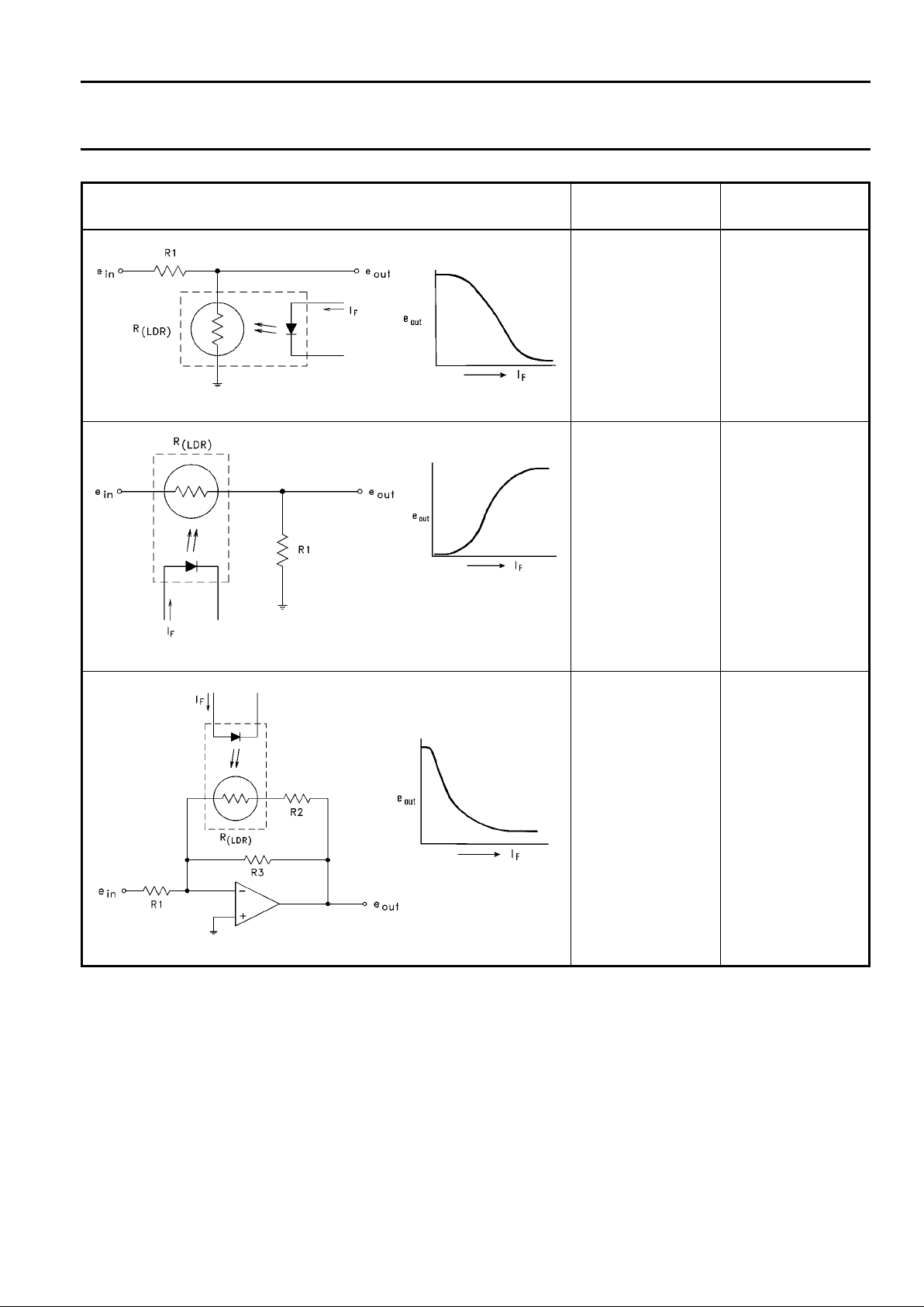
58
Application Notes—Analog Optical Isolators
Basic Circuit Configuration
Input
Resistance
Gain
Figure 1a. Shunt Input Control
Variable
Figure 1b. Series Input Control
Variable
Figure 1c. Feedback Resistor Control
Fixed, Low
e
out
e
in
------ -----
R
LDR()
R1R
LDR()
+
---------------------------
R
1
R1R
LDR()
+
---------------------------
R3R
LDRR2
+[]
1RLDRR2
R
3
++[
]
--------------------------------------------
Page 64
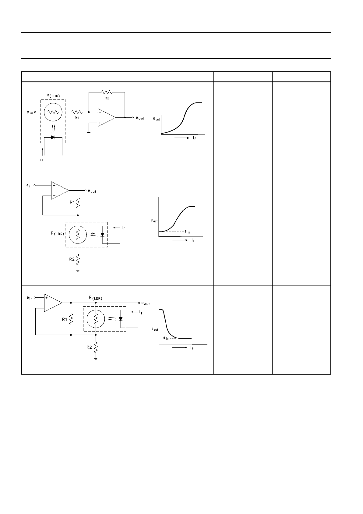
59
Application Notes—Analog Optical Isolators
Basic Circuit Configuration Input Resistance Gain
Figure 1d. Input Resistor Control
Variable
Figure 1e. Potentiometric Gain
Fixed, High
Figure 1f. Potentiometric Gain
Fixed, High
R
2
R
LDR()R1
+
---------------------------
1
R
1
R
LDR()R2
+
---------------------------+
R1R
LDR()
R2R
LDR()R1
+[
--------------------------------------+
Page 65
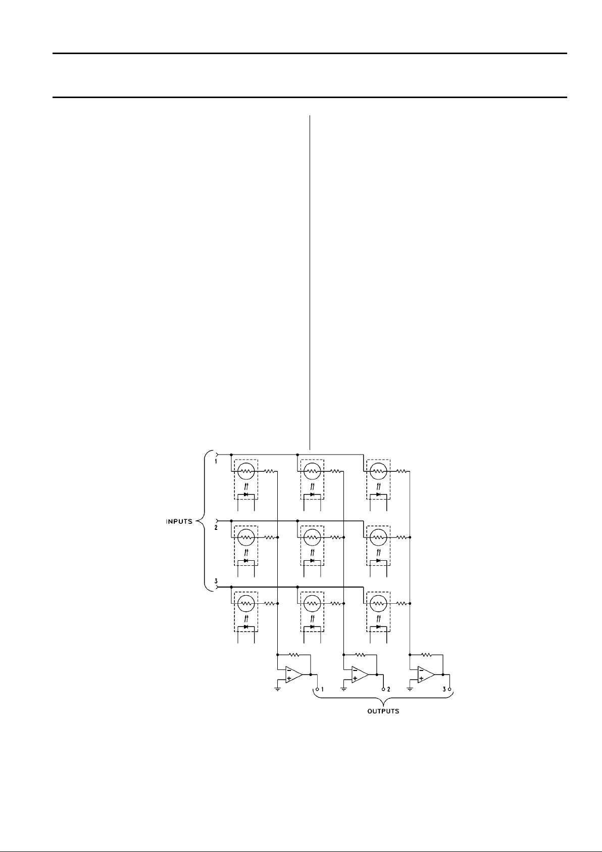
60
Application Notes—Analog Optical Isolators
Switching
Mechanical switching of low level audio signals requires the use of
switches with precious metal contacts. Sudden changes in signal can
cause the speakers to thump and damage may occur if the speaker is
underdamped. A simple way to avoid these problems is to use an AOI
in place of a mechanical switch. In the circuit of Figure 1d, the initial
resistance of the LDR cell is so high that amplifier gain is essentially
zero. A step change in forward current through the LED is translated
into a slower time change in the cell resistance. The resistance drops
to 10 times the final value in one millisecond or less. As the resistance
continues to drop, the final value is approached exponentially. Express
in terms of conductivity:
where:
G = conductance , mhos
t = time, ms
tc = time constance of the photocell, ms
If R1 is made equal to nine times the final value of resistance, the
response to 50% signal will occur in 1.0 ms. The time to get to within
0.5 db of full signal is one time constant, which is usually only a few
milliseconds. The step change of a switch has been transformed into a
rapid but smooth increase in signal level. In addition, the possibility of
turn-on in the middl e of a pea k has been eliminated.
Turn-off is slower and depends on the ratio of R1 to the final value of
photocell resistance. A high ratio will s low down the turn-off and speed
up the turn-on.
This circuit can be extended into a matrix as shown in Figure 2. While
a 3 x 3 matrix is shown, the number of nodes is not limited. Individual
inputs can be summed into a single output or connected to more than
one output. A matrix can be made very compact with the output
amplifiers mounted very close to reduce pickup. The op-amps
eliminate any crosstalk between the inputs since the summing point is
at virtual ground.
The controls for the matrix are usually remotely located. The DC
current through the LEDs may be controlled by switches, manual
potentiometers, or a comput er. The mat rix may be used for simple ONOFF gating, summing of several signals, or proportional control. When
proportional control is used, the output should be continuously
supervised to correct for changes in signal level due to photocell
resistance variation from temperature, light adapt history, and self
heating.
Figure 2. Switching Matrix
GG01 exp t– tc⁄()–[] mhos=
and: R 1 G ohms⁄=
Page 66
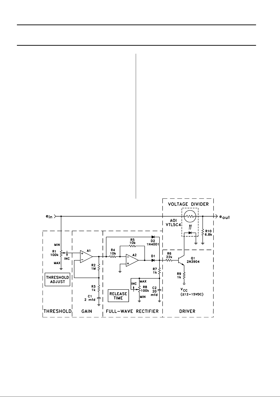
61
Application Notes—Analog Optical Isolators
Gating and Muting
Background noise becomes v ery ob jectionable when a si gnal level i n a
program is low. Noise is any unwanted sound and may be due to tape
hiss or amplifier hum. These noi ses can be eliminated by selective use
of gating and muting, that is, turning the amplifier on when the signal
level is high and off when it is low. This technique can also remove or
reduce unwanted echo , print through, presence or any other distracting
signal during portions of a program which are normally silent. The
gating circuit must be completely transparent to the listener, having a
smooth, rapi d operation with no signal dist ortion.
A pra ctical g ating ci rcuit h aving th ese feat ures is sh own in Fi gure 3.
The circuit has five basic sections: the threshold adjustment, a high AC
gain stage, full-wave rectifier, LED driver and an electrically controlled
voltage divider. When the signal is below the threshold level, the
voltage divider consisting of the AOI and R
10
has maximum
attenuat ion. When the signal exce eds th e threshold, the vol tage divider
allows the signal to pass through.
The circuit operation is as follows. The THRESHOLD potentiometer
applies a portion of the signal to the high gain AC amplifier consisting
of op-amp A
1
, resistors R2 and R3 and capacitor C1. The amplified
signal is full-wave rectified by diodes D
1
and D2 together with op-amp
A
2
which inverts the negative half of the signal. The rectifier charges
C2 used for RELEASE TIME control and drives the base of transistor
Q1, the LED driver. The threshold voltage is a sum of the forward drop
of the rectifying diodes, the voltage drop across R
6
, VBE or Q1 and V
F
of the LED. This voltage is 2.5 – 3.0V and when referred to the input
gives a thre shold of 2.5 – 3.0 mV at the amplifier.
The circuit can be set up for a specified threshold voltage. Release
time is usually determined empirically. A typical set up procedure uses
an audio signal containing spoken dialog. Initially, the THRESHOLD
adjustment is set to the maximum and the RELEASE is set to the
minimum. The program is turned on and the THRESHOLD is
decreased until the audio starts coming through, but sounds chopped
up. The chopping occurs because the circuit is too fast on r elease. The
RELEASE is increased until the audio is smoothed out and sounds
normal. Setting of the two controls needs to be made carefully. A
threshold set too high cuts off th e quieter sounds , while a setting whic h
is too low allows mor e of the noise to come throug h. Short release time
causes more chopping of the audio and can create some distortion at
the lower frequencies. Long re lease time keeps the gate open too long
allowing noise to come through after the signal is gone. Adjustments
should be made incrementally and worked between the two controls
until the best sound is achieved.
Figure 3. Audio Sound Gate
Page 67
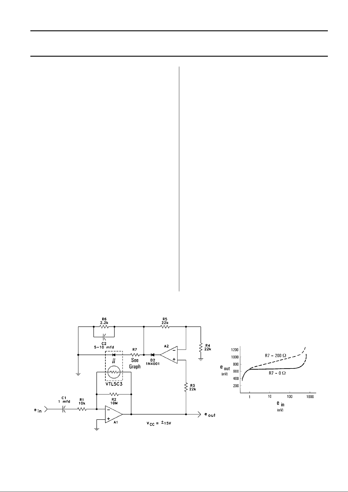
62
Application Notes—Analog Optical Isolators
Limiters
If the magnitude of an AC signal varies over a wide range, it may be
necessary to amplify or compress the signal before any audio
processing can be performed. In other cases, the audio power has to
be limited to prevent damage to an output device. Circuits that perform
this funct ion on a contin ual basis need a non-linear elem ent to produce
variable gain. However, most non-linear elements introduce distortion.
This is unacceptable in a high fidelity audio circuit and other critical
applications. Using an AOI, simple cir c uits can be made to perform this
function with out introducing distortion or ge ner ating any noise.
Signal Limiters
Any circu it that performs as a limiter or compressor must have lo w gain
when the signal magnitude is high and high gain when the signal is
low. The gain is adjusted so that a wide dynamic range is compressed
into a small one. In other signal processing applications, the signal
may need to be virtually constant.
The circuit such as shown in Figure 4a will keep the output level
constant when the input voltage varies over a range of 50 – 60 db.
Amplifi er A1 operates as an inv erting am plifier with a gain:
e
out
/ ein = R
PHOTOCELL
/ R
1
The feedback resistor is a photocell and has an “off ” resistance of 10
megohms , mi nimum, and an “on” resistance of 5000 ohms with 5.0 mA
in the LED. Using the components shown, the gain of this stage varies
between 500 with no signal and 0.5 with maximum signal applied. R
2
limits the maximum gain and is needed to prevent the amplifier, A
1
from going open loop when there is no input signal, in which case the
cell “off” resistance is much higher than 10 MΩ.
Amplifie r A
2
operates as a high input impedance rectifier that drives
the LED. The forward dro p of the LED is 1. 6 – 2.0V, and when the peak
output of the rectifier exceeds this value, current will flow into the LED.
As the signal increases, more current flows into the LED, driving the
photocell resistance lower thus decreasing the amplifier gain. The
output of A
1
is regulated at a v oltage determined by the f orward drop o f
the LED and the closed loop gain of amplifier A2. A2 amplifies the
signal by a factor of two, and a 1.8V peak (1.27 VRMS) is required to
activate this AOI. This results in the output voltage being held to 0.64
VRMS over a input range of 1 – 600 mV. Changing the value of R
4
changes the gain of the rectifier. Omitting R4 will double the output
voltage because the rectifier gain drops to one. Putting a resistor in
series with t he LED will cause the regulated vo lt age to rise as the inpu t
is increased (see Figure 4b). As the amplifier gain changes, the
amplifier bandwidth also changes. When the signal is low, the amplifier
will hav e the highest gain and low est bandwidth.
Figure 4a. Peak Sensing Compressor Figure 4b. Output Characteristics
Page 68
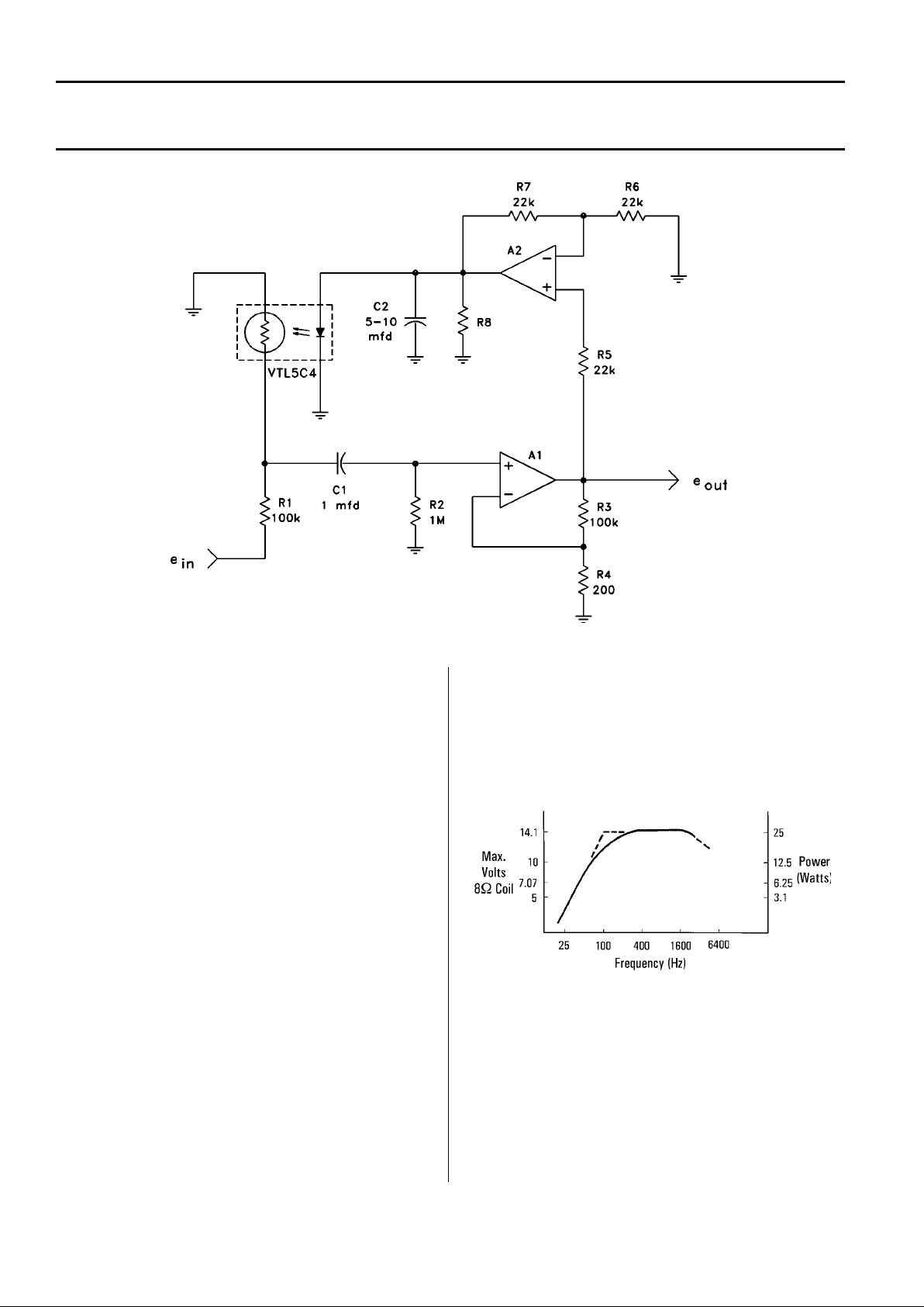
63
Application Notes—Analog Optical Isolators
Figure 5. Peak Sensing Compressor with Constant Bandwidth
Variable bandwidth can be avoided if the AOI is used in a voltage
divider circuit at the input of a fixed gain amplifier. For the same range
of input signals, the amplifier gain must be 500 and the voltage divider
must have a range of 1000:1. This configuration is shown in Figure 5.
The AOI has been changed to a lower resistance unit to be able to
work over the wider range. Also, A1 is now a high input impedance,
non-inverting stage to avoid a high insertion loss. This circuit is useful
when the input voltage is high, which allows the use of a lower gain
amplifier.
Speaker Power Limiting
Speakers th at are driven from high power amplifiers mu st be protected
from excess drive. While ordinary program levels may be well within
the rating of the speaker, peaks do occur that can be destructive. The
simplest solution is to use a compressor or limiter. Unfortunately, the
maximum power that may be applied is not constant over the
frequency range. Therefore, the limit must be set to provide protection
at the lowest frequency that is expected.
To understand the requirements for effective speaker pr ot ection, a brief
review of speaker power limitations follows. Figure 7 is a typical
maximum sine wave voltage limit for a low frequency speaker
commonly called a “woofer”. Above 200 Hz, the maximum allowed
voltage or power is constant. The operating temperature at which wire
insulation and coil bonding fail establishes this value. Below 200 Hz,
the voltage limit is determined by the allowable diaphragm excursion.
For constant voltage on the speaker, the displacement doubles when
the frequency is reduced by half. The maximum displacement is
determined by the mechanical design of the speaker and exceeding
the limit will produce extreme distortion and may even cause
mechanical damage.
Figure 7. Maximum sine wave V oltage and Power for a Typical Woofer
Page 69
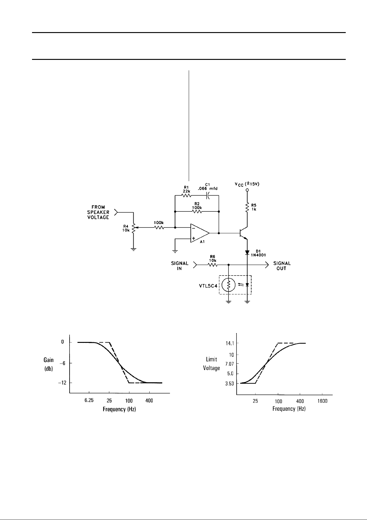
64
Application Notes—Analog Optical Isolators
This reduced low frequency power rating can be accommodated by
using a limited circuit which reduces the limit threshold when the
frequency is be low 200 Hz. Figure 8a shows a very simple circuit to do
this. At low frequency, the gain of amplifier A
1
is unity. The amplifier
has a 6 db/octave gain roll-off star ting at 25 Hz and levels off at 100
Hz. Therefore it will take a signal that is four times as large at 100 Hz
as at 25 Hz before limiting action starts. Breakpoints in the Frequency
vs. Gain curve shown in Figure 8b can be set to match the speaker
frequency dependent power limit. Also, potentiometer R4 can be set to
match the po w er rating and impedance of the speaker.
The threshold is set by the sum of V
BE
of Q1 and the forward voltage
drops of D1 and the LED, approximately 2.8V peak or 2.0 VRMS. Once
the threshold has been exceeded, current is injected into the LED of
the AOI which attenuates the signal voltage. This voltage divider can
be placed anywhere in the signal path. Once the limiter comes into
play, the system frequency response will no longer be flat, but no
distortion is introdu ced.
Automatic Gain Control
Automatic gain control (AGC) circuits have electrically programmable
references or set points, but in other respects are the same as limiters
or compressor circuits. Each has a forward gain amplifier and a loop
which controls the gain of that amplifier.
Figure 8a. Speaker Power Limiter with Frequency Compensation
Figure 8b. Amplitude vs. Frequency for the Amplifier Figure 8c. System Voltage Limits
Page 70
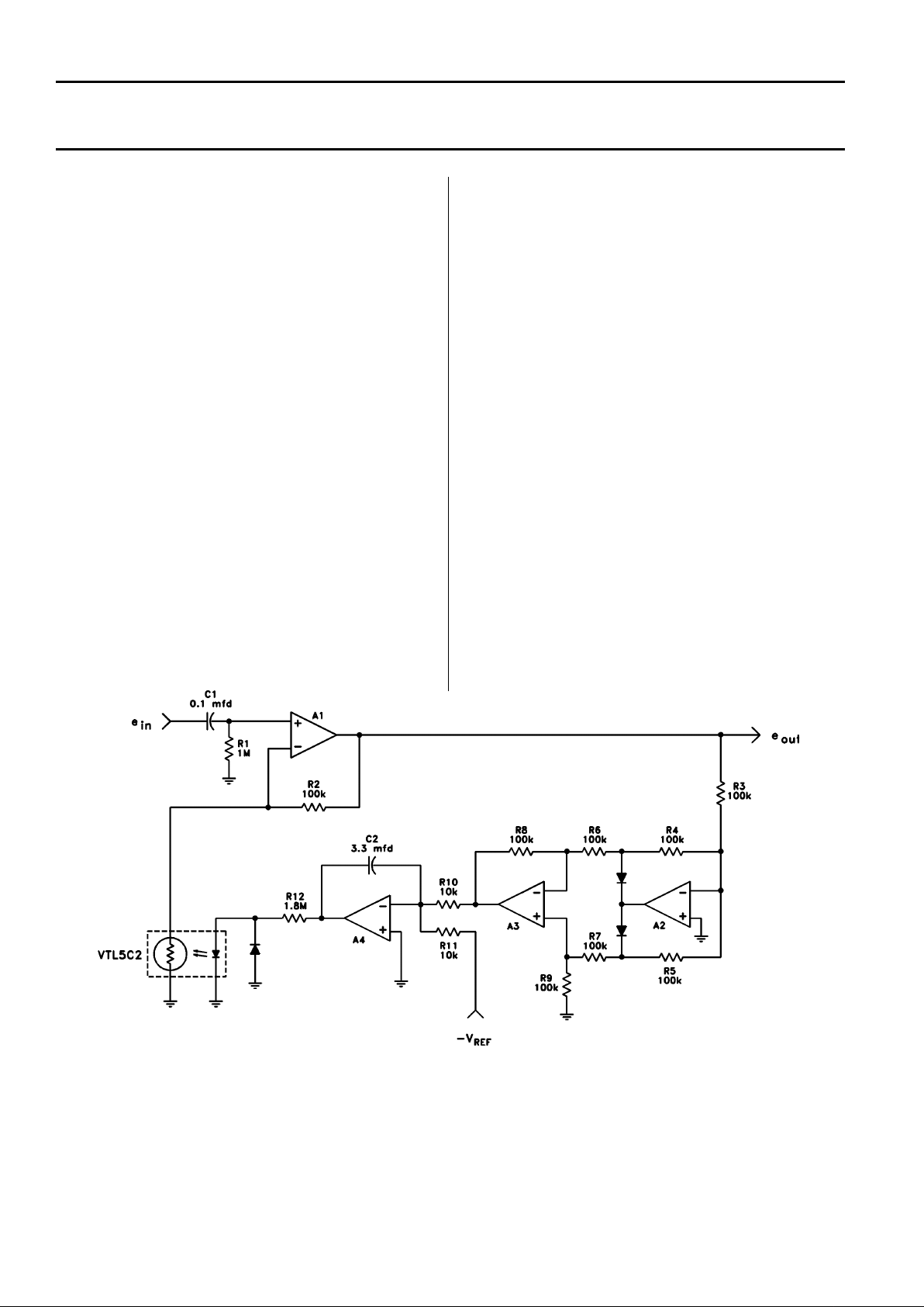
65
Application Notes—Analog Optical Isolators
Figure 9 shows an AGC circuit which consists of three main elements:
a variable gain amplifier, full-wave active rectifier and a summing
amplifier. The variable gain amplifier consists of op-amp A1 with
potentiometric gain that is controlled by the resistance of the photocell
of the AOI. The gain of this amplifier is:
Gain = 1 + R
2
/ R
PHOTOCELL
With R2 = 100k ohms, the minimum gain is one since the cell “off”
resistance is several megohms. The maximum gain in only 100 since
the resistance of a typical VTL5C2 is 1000 ohms at an input current of
5.0 mA. If a range of 40 db (100:1) is not adequate, there are several
options. R
2
can be increased, the LED drive current for the AOI can be
increased or a lower resistance AOI such as the VTL5C4 can be used.
Amplifie r A
2
together with diodes D1 and D2 and resistors R3, R4, and
R5 form a full-wave rectifier. The amplifier has a gain of one so the
output is equal to the rectified input. There is no offset due to rectifier
forward drops so this circuit will rectify signal s all the way down to zero
volts. Since the DC output of A2 is not referenced to ground, op-amp
A3 and resistors R6, R7, R8, and R9 form a fully differential amplifier
which shifts the DC reference to ground.
Op-amp A
4
is used as an integrator. The signal from the full-wave
rectifier is summed with a reference voltage V
REF
and integrated. The
time constant of the integrator is selected to limit the bandwidth of the
control loop as well as assure stability of the loop. If the bandwidth is
too wide, the control loop will follow the signal on an instantaneous
basis. The AOI alone i s not very fast, but signals wit h frequencies of 30
– 60 Hz could be distorted if ther e w ere no time delay in the integrator.
The AGC circuit operates as follows. When there is no signal, the
negative V
REF
causes A4 to be at a maximum positive output.
Maximum forward current is injected into the LED, driving the cell to a
low resistance and the gain of A
1
to the maximum where it stays until
there is a signal. A si gnal at the input terminal is amplified, r ectified and
algebraically summed with V
REF
at the inverting terminal of the
integrator. The control loop will then act to make the absolute value of
the rectifi ed signal equal to the reference v olt age. V
REF
may be a fixed
value or a function of some other param eter.
Electrically Controlled Gain
The gain of an amplifier can be electrically programmed using the
circuit of Figure 10. An AOI w it h a center tapped photocell is used, one
side in the signal amplifier channel and the other in the control loop.
The signal amplifier consists of op-amp A1, resistors R3 and R2 which
set the gain and the input resistor R
5
. The gain of this amplifier is given
by:
Figure 9. AGC Circuit with Electrical Setpoint
G
e
out
e
in
--------
R2R3+()
R
2
----------------------==
Page 71
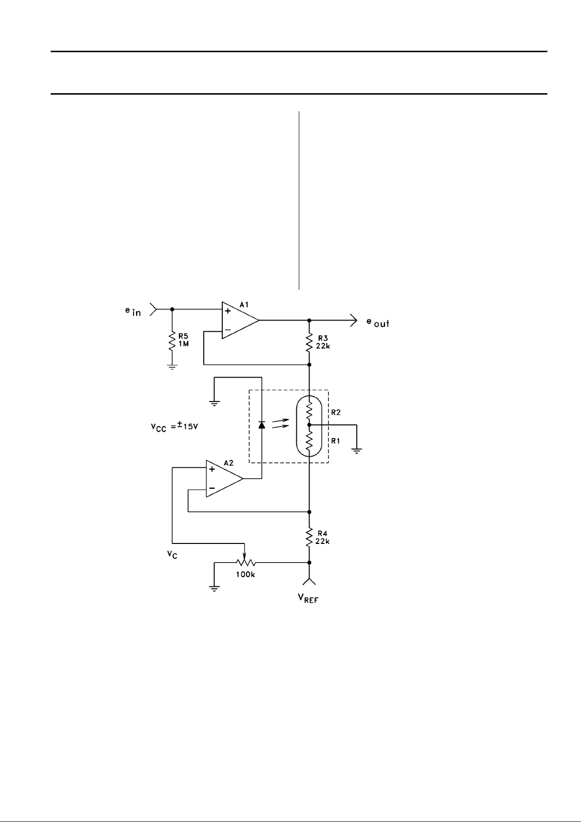
66
Application Notes—Analog Optical Isolators
The control loop consists of op-amp A2 and resistors R1 and R4. This
circuit sets the LED current so that:
If we set: R
3
= R
4
and: R1 = R
2
then: e
out
/ ein = V
REF
/ V
C
or: e
out
= ein (V
REF
/ VC)
where V
C
= control voltage
Note that R
1
and R2 are the two halves of the cell . These two resistors
match within 10% and track over a wide range within 5% so that the
gain is closely set by VC when V
REF
is fixed.
The limits of ope ration are:
0 < V
C
< V
REF
and the signal must never be so large that amplifier A1 saturate s when
the gain is at maximum.
This circuit performs a dividing operation with e
in
and VC as the
numerator and denominator respectively. The accuracy is limited by
the tracking ability of the two sides of the photocell. The error due to
matching can be eliminated by trimming R
4
.
Figure 10. Electrically Programmable Gain
V
REF
V
C
-----------
R1R4+()
R
1
----------------------=
e
out
e
in
--------
V
REF
V
C
----------- Gain==
Page 72
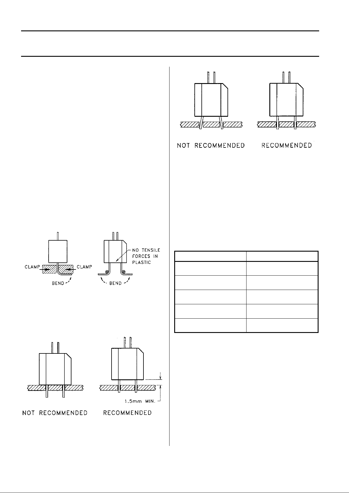
67
Application Notes—Analog Optical Isolators
APPLICATION NOTE #2
Handling and Soldering AOIs
All opto components must be handled and soldered with care,
especially those that use a cast or molded plastic and lead frame
construction li ke the LEDs used in AOIs.
In LED lead frame construction, the emitter chip is mounted directly to
one lead and a wire bond is made from the chip to the other lead. The
encapsulating plastic is the only support for the lead frame. Care must
be taken when forming the leads of plastic opto packages. Excessive
mechanical force can cause the leads to move inside the plastic
package and damage the wire bonds. Weakened bonds can then
“open up” under further mechanical or thermal stressing, producing
open circuits .
In order to form leads safely, it is necessary to firmly lamp the leads
near the base of the package in order not to transfer any force
(particularly tension forces) to the plastic body. This can be
accomplished either through use of properly designed tooling or by
firmly gripping the leads below the base of the package with a pair of
needle nose pliers while the leads are bein g bent .
Examples of T ooling Fixtures Used to Form Leads
For highest reliability, avoid flush mounting the A O I body on the printed
circuit board. This minimizes mechanical stress set up between the
circuit board and the LED and photocell packages. It also reduces
solder head damage to the packages.
Good printed circuit board layout avoids putting any spreading (plastic
under tension) force on the leads of the LE D and photocell.
When hand solde ring, it is important to limit the maximum temperature
of the iron by controlling the power. It is best if a 15W or 25W iron is
used. The maximum recommended lead soldering temperature (1/16"
from the case for 5 seconds) is 260°C. An RMA rosin core solder is
recommended.
Sn60 (60% tin / 40% lead) solder is recommended for wave soldering
opto components into printed circuit boards. Other alternatives are
Sn62 and Sn63. The maximum recommended soldering temperature
is 260°C with a maximum duration of 5seconds.
The amount of tarnish on the leads determines the type of flux to use
when soldering devices with silver plated leads.
Cleaners designed for the removal of tarnish from the leads of
electronic components are acidic and it is best to keep the immersion
time as short as possible (less than 2 seconds) and to immediately
wash all devices thoroughly in ten rinses of deionized water.
Condition of Lead s Recommended Flux
Clear Bright Finish
(T arnish Free)
RMA - Mildly Activated
Dull Finish
(Minimal Tarnish)
RMA - Mildly Activated
Light Yellow Tint
(Mild Tarnish)
RA - Activated
Light Yellow / Tan Color
(Moderate Tarnish)
AC - Water Soluble,
Organic Acid Flux
Dark Tan / Black Color
(Heavy Tarnish)
Leads Need to be Cleaned
Prior to Soldering
Page 73
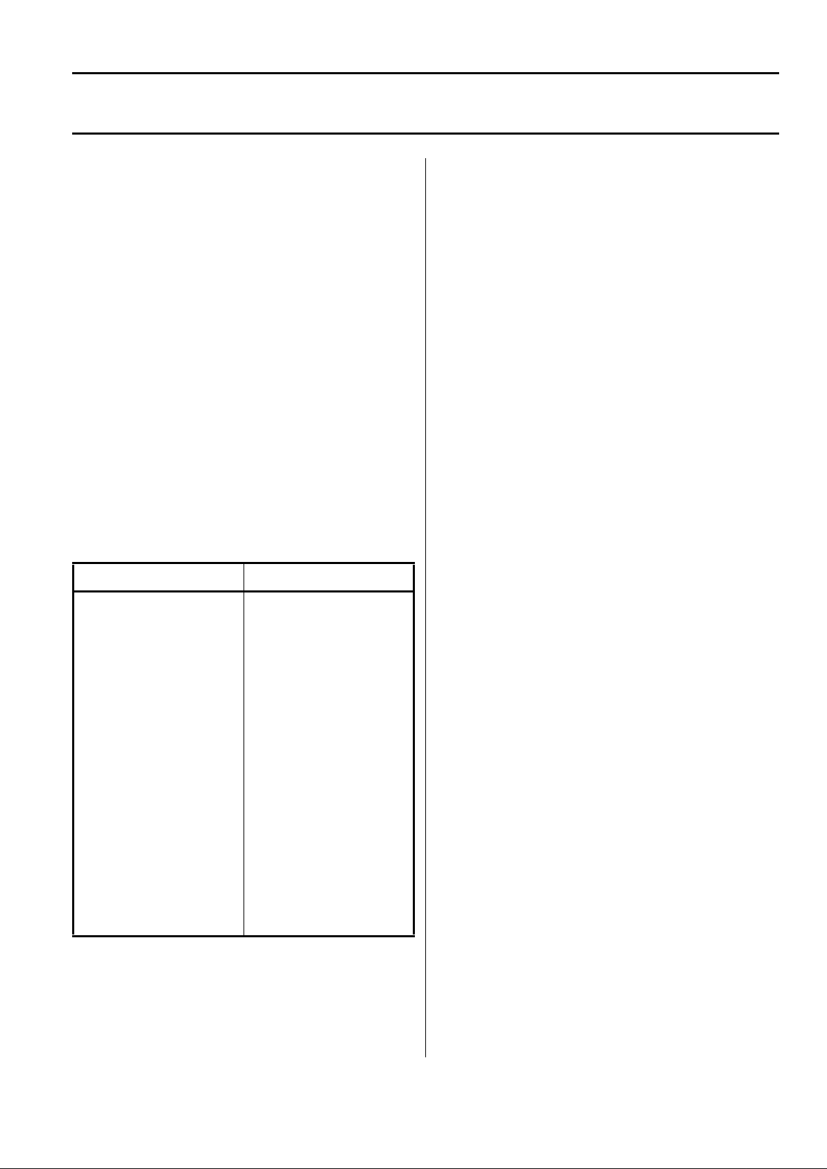
68
Application Notes—Analog Optical Isolators
The best policy is one which prevents tarnish from forming. Tar nish,
which is a compound formed when silver reacts with sul fur (Ag2S), can
be prevented by keeping the components away from sulfur or sulfur
compounds. Since two major sources of sulfur are room air and paper
products, it is best to store the devices in pr otective packag ing such as
a “silver saver” paper or tigh tly sealed polyethylene bags.
After soldering, it is necessary to clean the components to remove any
rosin and io nic residues. For a listing of re com m ended cleaning agent s
please refer to Application Notes #3.
APPLICATION NOTE #3
Recommended Cleaning Agents
The construction of an AOI consists of a cast epoxy LED, ceramic
photocell, a molded case and epoxy as the end fill. This construction
allows a wide variety of cleaning agents to be sued after soldering.
In many cases the devices will be exposed to a post solder cleaning
operation which uses one or more solvents to remove the residual
solder flux and ionic contaminants. Only certain cleaning solvents are
compatible with the plastics used in the A OI packages.
This listing of recommended/not recommended solvents represents
only a very small percentage of available chemical cleaning agents.
Even with this list of recommended solvents it is important to be aware
that:
1. Solvent exposure times should be as short as possible.
2. The exact requirement of the cleanin g process will vary from
customer to custom er and application to applic ati on.
3. Additiv es and concentrations will vary from supplier to supplier.
Because of these uncertainties, our recommendation is that all
customers careful ly ev al uate their own cleaning pro cess and dra w their
own conclusions about the effectiveness and reliability of the process.
PerkinElmer cannot assume any responsibility for damage caused by
the use of any of the solvents above or any other solvents used in a
cleaning process.
Recommended Not Recommended
Arklone A Acetone
Arklone K Carbon Tetrachloride
Arklone F Methyl Ethyl Ketone
Blaco-Tron DE-15 Methylene Chloride
Blaco-Tron DI-15 Trichloroeth ylene (TCE)
Freon TE Xylene
Freon TES Trichloroethane FC-111
Freon TE-35 Trichloroethane FC-112
Freon TP Freon TF
Freon TF-35 Freon TA
Genesolv D Freon TMC
Genesolv DE-15 Freon TMS
Genesolv DI-15 Genesolv DA
Isopropyl Alcohol Genesolv DM
Water Genesolv DMS
Page 74

PerkinElmer Optoelectronics warrants that all items sold will be free from defects in materials and
workmanship under normal use and service for a period of one year from the date of shipment. If
PerkinElmer Optoelectronics receives notice of such defects during the warranty period, PerkinElmer
Optoelectronics shall, at its option, repair or replace any defective components or credit the purchaser's
account with the purchase price paid. This warranty shall not apply to items that have been (a) subject
to misuse, neglect, accident, damage in transit, abuse or unusual hazard; (b) altered, modified or
repaired by anyone other than PerkinElmer Optoelectronics; or (c) used in violation of instructions
furnished by PerkinElmer Optoelectronics. The Buyer should contact PerkinElmer Optoelectronics for a
return authorization number prior to shipping returned parts.
The specific PerkinElmer Optoelectronics' products shown in this catalog are not authorized or
recommended for use as critical components in life support systems or in surgical implant devices
wherein a failure or malfunction of the PerkinElmer Optoelectronics product may directly threaten life or
cause personal injury. The Buyer agrees to notify PerkinElmer Optoelectronics of any such intended
application and to proceed only after receiving the expressed written approval of an officer of
PerkinElmer Optoelectronics. Additionally, the user of PerkinElmer Optoelectronics components in life
support or implant applications assumes all risks of such use and indemnifies PerkinElmer
Optoelectronics against all damages.
In order to provide the best possible products, PerkinElmer Optoelectronics reserves the right to change
specifications without prior notice. Information supplied in PerkinElmer Optoelectronics' catalogs, data
sheets, and other literature, and information supplied by PerkinElmer Optoelectronics' technical support
personnel is believed to be reliable, however, PerkinElmer Optoelectronics cannot assume responsibility
for omissions, errors, or misapplication of this information.
It is the responsibility of the Buyer to determine the suitability of PerkinElmer Optoelectronics/ products
and recommendations in his own specific application, particularly when the products are operated at or
near their maximum rating specifications. No license is granted by implication or otherwise of any
patent, copyright, or trademark right of PerkinElmer Optoelectronics or others.
PerkinElmer Optoelectronics' warranty, as stated above, shall not be affected or changed by, and no
obligation or liability shall grow out of, PerkinElmer Optoelectronics' providing technical advice or service
to the Buyer.
PERKINELMER OPTOELECTRONICS MAKES NO OTHER WARRANTIES, EXPRESSED OR
IMPLIED, AND EXPRESSLY EXCLUDES AND DISCLAIMS ANY WARRANTIES OF
MERCHANTABILITY OR FITNESS FOR A PARTICULAR PURPOSE. THE REMEDIES PROVIDED
HEREIN ARE THE BUYER'S SOLE EXCLUSIVE REMEDIES. PERKINELMER OPTOELECTRONICS
SHALL NOT BE LIABLE FOR ANY INDIRECT, SPECIAL, INCIDENTAL, OR CONSEQUENTIAL
DAMAGES, WHETHER BASED ON CONTRACT, TORT, OR ANY LEGAL THEORY. PERKINELMER
OPTOELECTRONICS' LIABILITY ON ANY CLAIM SHALL IN NO CASE EXCEED THE PRICE
ALLOCABLE TO THE ITEM WHICH GIVES RISE TO THE CLAIM.
PerkinElmer Optoelectronics
Warranty Statement
Page 75
PerkinElmer Optoelectronics’ business is the design, development, and production of optoelectronic components
and assemblies. Our development and manufacturing activities focus on achieving and maintaining consistent
product quality and high levels of reliability. PerkinElmer produces devices and assemblies for the commercial,
industrial, automotive, and medical markets.
PerkinElmer’s commitment to quality emphasizes designed-in quality, problem prevention, and closed loop corrective action. This concept of quality is implemented through the use of fully documented procedures, inprocess monitoring and process control (including SPC), and 100% production testing of devices using state-ofthe-art automated test equipment. As a world class manufacturer, PerkinElmer’s concept of product quality
includes Total Quality Management (TQM) and Just In Time (JIT) delivery.
Quality is a measure of how well a device conforms to its specifications. Reliability is a measure of how well a
device performs over time. PerkinElmer insures the reliability of its products by careful design and by the periodic testing of random samples taken from the manufacturing lines. Reliability tests include temperature cycles,
thermal shock, room ambient life tests, elevated temperature life tests, high and low temperature storage, temperature/humidity tests, and water immersion.
PerkinElmer also performs special tests covering a wide range of environmental and life stress conditions to
support non-standard, custom applications. The information generated not only assures the customer that the
device will work well in a particular application, but also contributes to our data base for continual product
improvement.
Driven by our goal of continuous improvement and the needs of customers, PerkinElmer runs an active product
improvement program. PerkinElmer continuously evaluates new materials, manufacturing processes, and packaging systems in order to provide our customers with the best possible product.
PerkinElmer’s quality works: we are an ISO 9000 and QS 9000 certified supplier (ship to stock - no inspection
required) to a number of major customers.
Quality Statement
Page 76

.
© 2001 PerkinElmer, Inc. All rights reserved. CA-274 Rev A1001
Additional Sensor Products Catalogs
USA:
PerkinElmer Optoelectronics
10900 Page Avenue
St. Louis, MO 63132
Phone: (314) 423-4900
Fax: (314) 423-3956
Europe:
PerkinElmer Optoelectronics
Wenzel-Jaksch-Str. 31
D-65199 Wiesbaden
Germany
Phone: +49 611 492 0
Fax: +49 611 492 170
Asia:
PerkinElmer Optoelectronics
Room 1404, Kodak House II
39 Healthy Street East
North Point, Hong Kong
Phone: 852 2590 0238
Fax: 852 2590 0513
www.perkinelmer.com/opto
 Loading...