

Page 1
Corporate: www.cdtechno.com
Corporate: www.cdtechno.com
Product: www.cdpowerelectronics.com
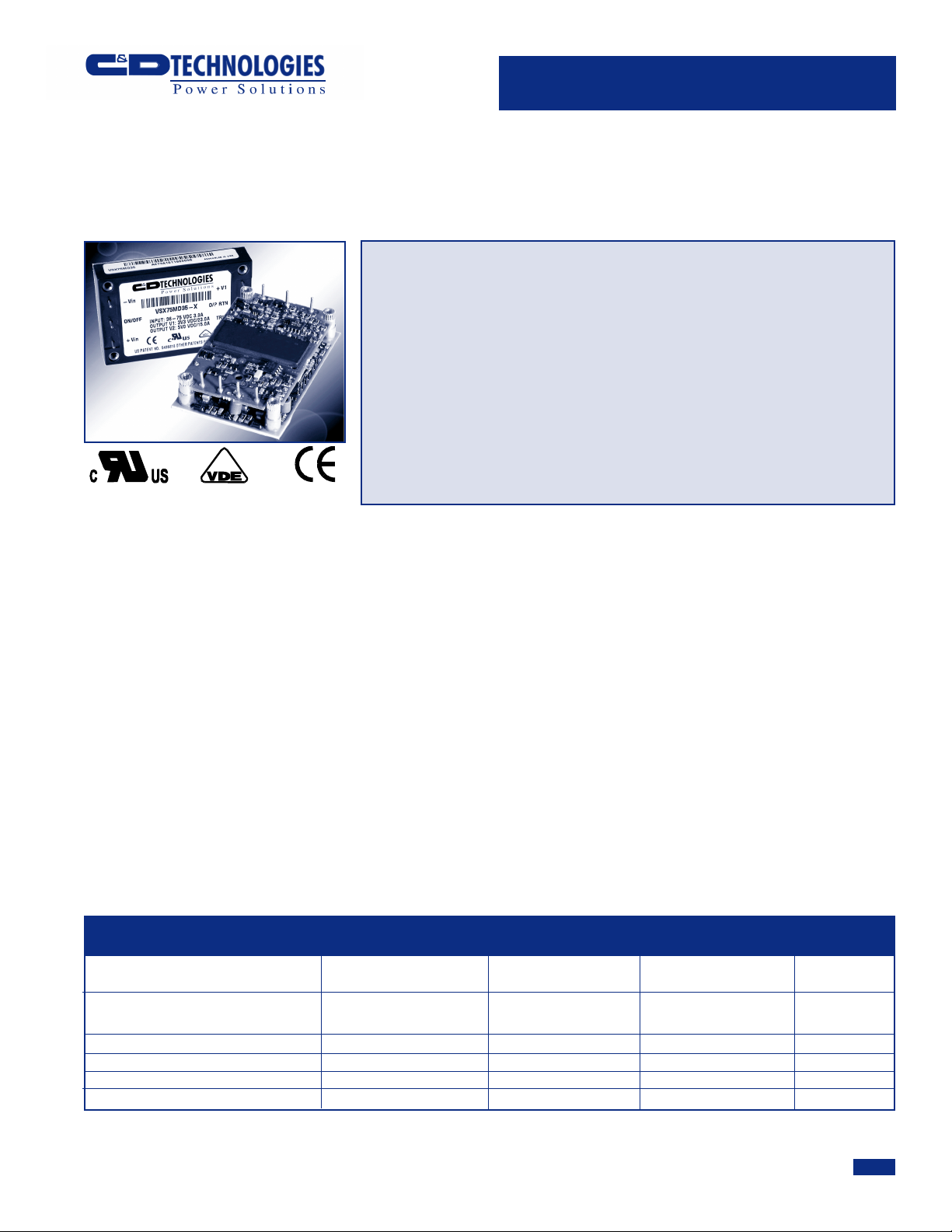
VSX75MD35
75 Watt Dual Output Quarter Brick DC/DC Converter
VSX75
VSX75-U
APPLICATIONS
Distributed Power Architectures
Workstations
EDP Equipment
Telecommunications
OPTIONS
Choice of Remote On/Off Logic
Configuration
Heatsink Available for Extended
Operation
3.3V & 5.0V Dual Output
2.3" x 1.5" x 0.5"
90% Efficiency
Low Output Noise
Input Filtering
Remote On/Off, Input Side
Output Voltage Trim, +/-10%
Fixed Frequency Operation
-40C° to +100C° Baseplate Temp.
Output Current Limit, Self-Start
1,500 Vdc Isolation, Input to Output
The VSX75 Series are 75 Watt, compact,
high-efficiency, high-density dual
output converters with a 36-75V input
and with 3.3Vdc and 5.0Vdc outputs.
The industry quarter-pack size of
2.3" x 1.5" x 0.5" coupled with 90%
efficiency is an industry high-density
breakthrough.
These converters utilize V Series high
density technology. This technology
has been featured in our highly efficient
VKP and VKA Series now successfully in
use worldwide. The very high 90%
UL/CUL 1950, EN60 950
36-75 Vdc Input Models
Continuous Short Circuit
Protection
Non-latching Protection:
Input Undervoltage
Input Overvoltage
Output Overvoltage
Overtemperature
Output Voltage Tracking at Turn-on
and Turn-off
No Minimum Load Current
efficiency minimizes the requirement for
heat-sinking and the low output ripple
minimizes the need for additional
filtering. For maximum flexibility, power
can be traded between outputs as
required. The VSX75 Series feature
virtually all of the options required by
design engineers but not at the
competition’s typical additional price
for each option. This multitude of
features are standard on the VSX75
Series.
ADDITIONAL INFORMATION
See Application Note DCAN-40
at www.cdpowerelectronics.com
ABSOLUTE MAXIMUM RATINGS
PARAMETER SYMBOL MIN MAX UNIT
Input Voltage:
VSX75MD35 Vi 100 Vd c
I/O Isolation Voltage 1500 Vdc
I/P to case 1500 Vdc
O/P to case 200 V dc
Operating Case Temperature T -40 100 °C
Product: www.cdpowerelectronics.com
VSX75MD35 REV B 5/02
1
Page 2
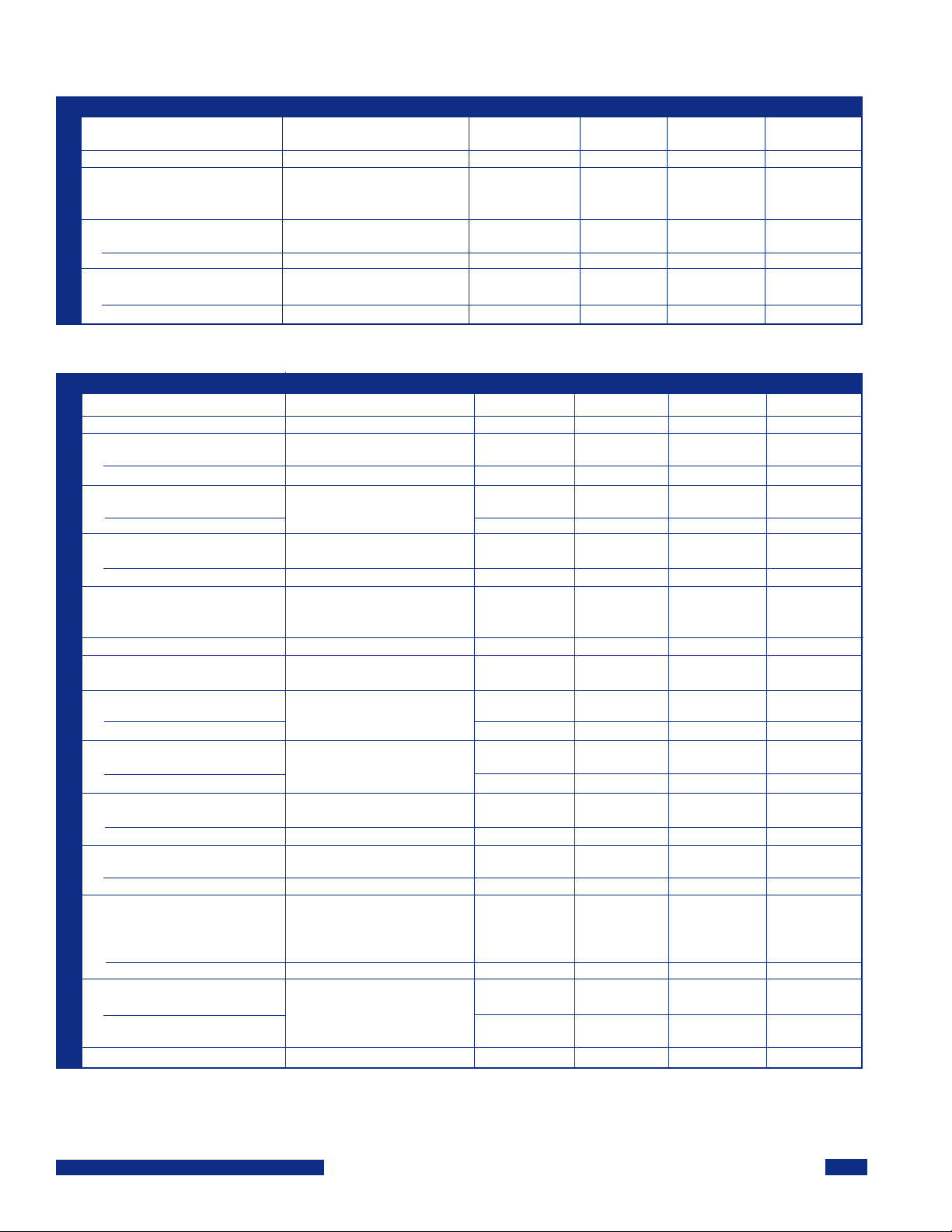
SPECIFICATIONS, ALL MODELS
Specifications are at T
PARAMETER SYMBOL MIN TYP MAX UNITS
INPUT
Voltage Range 36 48 75 VDC
Input Reflected Ripple Current Peak - Peak 500 mA
Maximum Input Current Vin = 30V, Pout 75W 3 A
No Load Input Current 60 mA
On/Off Activated Input Current 25 mA
Input Undervoltage Lockout
INPUT
Turn On 30 33 36 VDC
Turn Off 27 30 33 VDC
Input Overvoltage Lockout
Turn Off 76 80 84 VDC
Turn On 74.5 78.5 82.5 VDC
PARAMETER CONDITIONS MIN TYP MAX UNITS
Output Power 75 Watts
Output Efficiency Io1=11.5A, Io2=7.5A 89 %
Set Point Voltage
V1 (3.3V) Io1=11.5A 3.26 3.30 3.34 VDC
V2 (5.0V) Io2=7.5A 4.96 5.02 5.08 VDC
Output Current Total Module Output
V1 (3.3V) Power Should Not 0 23 A
V2 (5.0V) Exceed 75 Watts 0 15 A
Output Ripple And Noise Voltage 100 MHz BW
V1 (3.3V) 60 mV
V2 (5.30V) 80 mV
Output Adjust Range Both Outputs Will Adjust -8 +10 %
Output Temperature Drift . 0.02 0.05 % /°C
Line Regulation VIN = 36 to 75 0.10 0.20 %
Load Regulation
V1 (3.3V) I1= 0 to 23A, I2=0A 3.0 % of Nom
V2 (5.0V) I1=0A, I2=0 to 15A 2.5 % of Nom
Load Cross Regulation
V1 (3.3V) I1= 0A, I2=0 to 15A 1.0 % of Nom
V2 (5.0V) I1=0 to 23A, I2=0A 5.0 % of Nom
Output Current Limit Inception
V1 (3.3V) 24 27 30 A
V2 (5.0V) 16 18 20 A
Short Circuit Current
V1 (3.0V) 22 25 30 A
V2 (5.0V) 15 18 20 A
Output Overvoltage Set Point
(Non-latching independent
control loop)
V1 (3.3V) 3.8 4.0 4.3 VDC
V2 (5.0V) 5.85 6.1 6.35 VDC
Transient Response (∆Ιο/∆t=0.2A/µsec either
Settling Time output) Load change of 40% 100 µsec
OUTPUT Under any conditions, the voltage of V1 will always be greater or equal to that of V2.
Peak Deviation of Ιο max at any operating 4 %
Switching Frequency 330 KHz
= +40°C nominal input voltage unless otherwise specified.
CASE
at the Same Time and
by the Same %
I1=11.5A, I2=7.5A
load up to Ιο max and Pο max
P-P
P-P
Product: www.cdpowerelectronics.com
VSX75MD35 REV B 5/02
2
Page 3
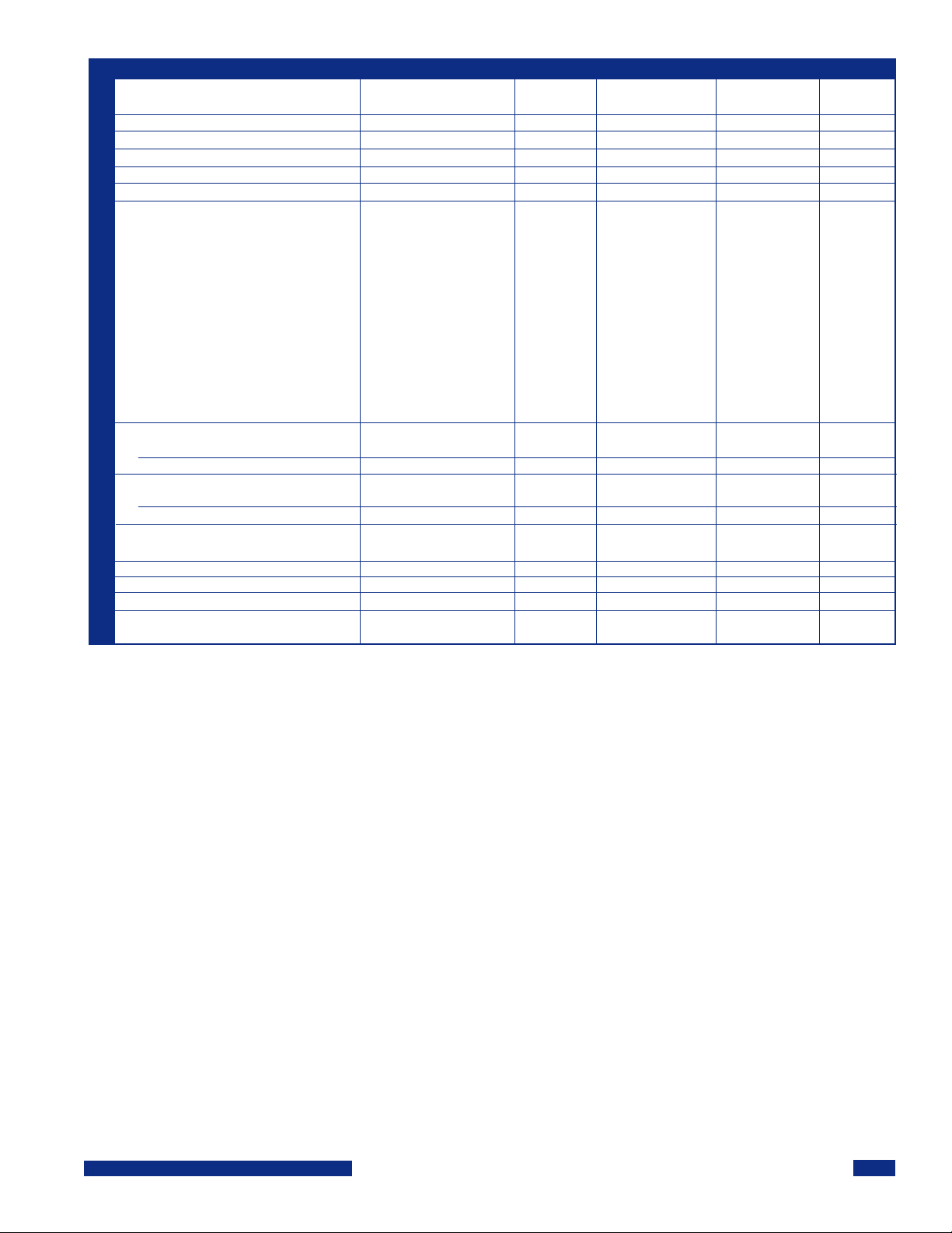
PARAMETER SYMBOL MIN TYP MAX UNITS
ISOLATION SPECIFICATIONS
Input to Output 1500 VDC
Input to Case 1500 VDC
Output to Case 200 VDC
Resistance Input to Output 10 MΩ
Capacitance Input to Output 1000 pF
Leakage Current V
FEATURE SPECIFICATIONS
Remote On/Off
(open collector equivalent,
signal referenced to –VIN terminal)
VSX75MD35 Preferred Logic (negative)
Logic Low – Module On
Logic High – Module Off
VSX75MD35-1 Optional Logic (Positive)
Logic Low – Module Off
Logic High – Module On
GENERAL
Turn On Time
From Application of V
From Remote On/Off Activation steady state) 3 4 mSecs
Weight
VSX75MD35, VSX75MD35-1 67 Grams
VSX75MD35-U, VSX75MD35-1U 44 Grams
TEMPERATURE
Operation /Specification Case -40 +100 ° C
Storage Case -55 +125 ° C
Shutdown Case +105 +115 +125 ° C
Shutdown (Hysteresis) 10 ° C
Thermal Impedance Free Air 12.2 ° C/Watt
(Case to Ambient)
IN
= 240VAC, 60Hz 90 µA, rms
ISO
Von/off Low 0 0.4 V
Von/off High 2 Open Collector VDC
Ιon/off 200 µA
(VO within 1% of 7 10 mSecs
DC
Product: www.cdpowerelectronics.com
VSX75MD35 REV B 5/02
3
Page 4
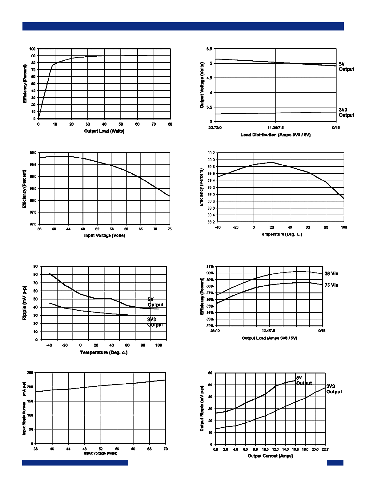
GRAPHS
EFFICIENCY VS. OUTPUT LOAD
EFFICIENCY VS. INPUT VOLTAGE
LOAD REGULATION VS. LOAD DISTRIBUTION
EFFICIENCY VS. BASEPLATE TEMPERATURE
OUTPUT VOLTAGE RIPPLE VS.
TEMPERATURE AT FULL LOAD
REFLECTED RIPPLE VS. INPUT VOLTAGE
FULL LOAD EFFICIENCY VS. LOAD DISTRIBUTION
OUTPUT RIPPLE VS. LOAD
Product: www.cdpowerelectronics.com
VSX75MD35 REV B 5/02
4
Page 5
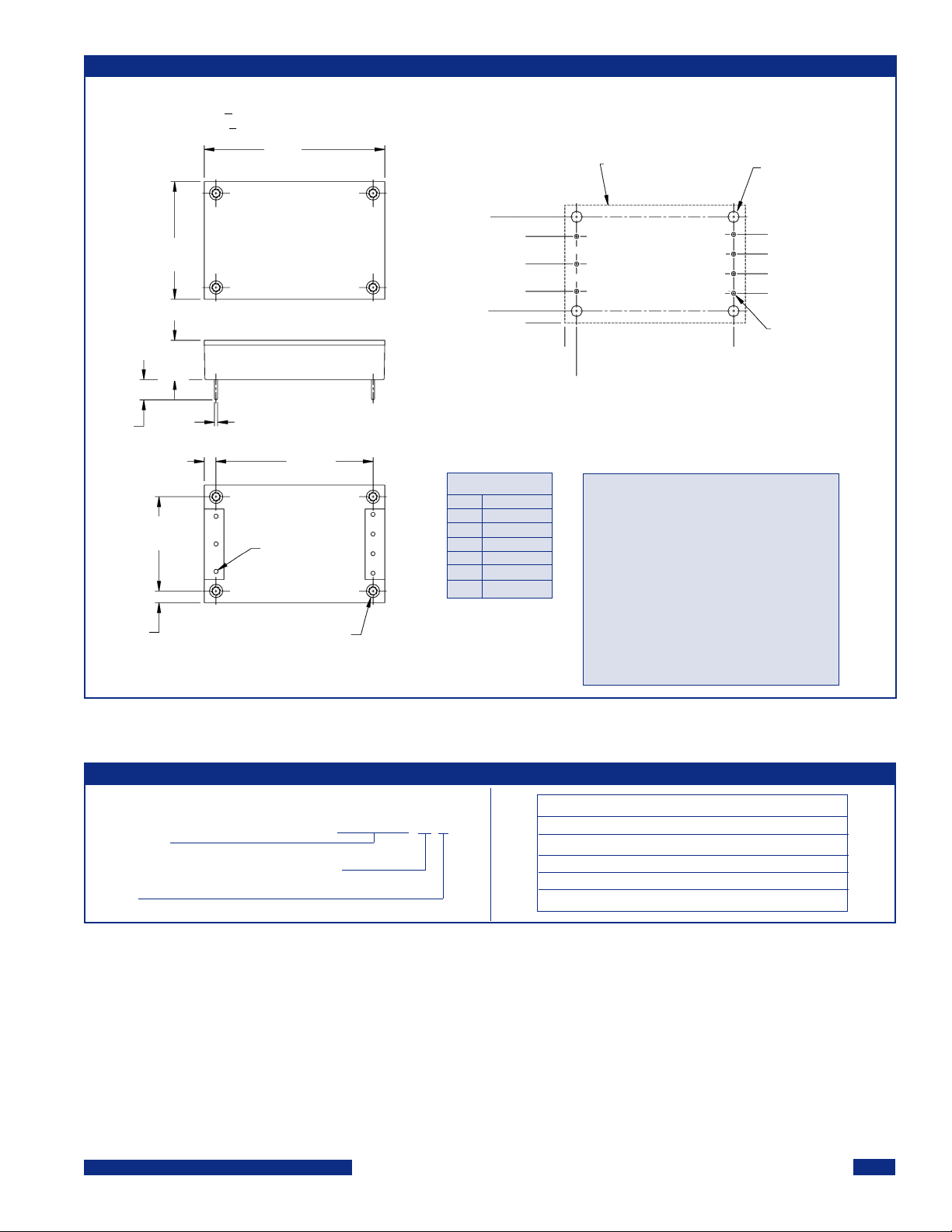
Dimensions are in inches (millimeters).
Tolerances: x.xx in. + 0.02 in.
x.xxx in. +0.01 in.
MECHANICAL
.145
(3.68)
(3.81)
.150
1.50
(38.10)
.50
(12.70)
.150
(3.81)
1.200
(30.48)
2.30
(58.42)
0.040 (1.02) 7 PLACES
2.000
(50.80)
PIN 1
M3 THREAD
4 PLACES
.600
(15.24)
.350
(8.89)
.000
.350
(8.89)
.600
(15.24)
.750
(19.05)
Pinout Key
1 +Vin
2 On/Off
3-Vin
4 +3.3 Vout
5 O/P RTN
6 Trim
7 +5.0 Vout
CASE OUTLINE
7
6
5
4
2.000
(50.80)
.150
1
2
3
(3.81)
.000
RECOMMENDED PCB HOLE PATTERN
(VIEW OF PCB, THROUGH UNIT)
NOTES:
1. Marked with: specific model ordered, date
code, job code.
2. MATERIAL: Units are encapsulated in a low
thermal resistance molding compound which has
excellent chemical resistance and electrical
properties in high humidity environments and
over a wide operating temperature range. The
encapsulant and outer shell of the unit have
UL94V-0 ratings. Lead material is solder plated
to allow ease of solderability.
3. IMPORTANT: When utilizing the PEM nuts for
board mounting, it is required to follow guidelines
in application note DCAN-40 available on the
web at www.cdpowerelectronics.com.
0.144 (3.66)
4 PLACES
.375 (9.53)
.125 (3.18)
.125 (3.18)
.375 (9.53)
0.051 (1.30)
7 PLACES
ORDERING INFORMATION
To Find Model Number
VSX75MD35 - 1 U
Device Family
VSX75MD35 (Quarter Brick, 75 Watt DC/DC)
Logic: No Number = Preferred Logic (Negative);
1 = Optional Logic (Positive)
Package
No Letter = Encapsulated; U = Unencapsulated
Power Electronics Division, United States
3400 E Britannia Drive, Tucson, Arizona 85706
Tel: 800.547.2537 Fax: 520.295.4160
Any data, prices, descriptions or specifications presented herein are subject to revision by C&D Technologies, Inc. without notice. While such information is believed to
be accurate as indicated herein, C&D Technologies, Inc. makes no warranty and hereby disclaims all warranties, express or implied, with regard to the accuracy or
completeness of such information. Further, because the product(s) featured herein may be used under conditions beyond its control, C&D Technologies, Inc. hereby
disclaims all warranties, either express or implied, concerning the fitness or suitability of such product(s) for any particular use or in any specific application or arising
from any course of dealing or usage of trade. The user is solely responsible for determining the suitability of the product(s) featured herein for user’s intended purpose
and in user’s specific application. C&D Technologies, Inc. does not warrant or recommend that any of its products be used in any life support or aviation or aerospace
applications.
Product: www.cdpowerelectronics.com
VSX75MD35 REV B 5/02
Tel: +44 (0)1908 615232 Fax: +44 (0)1908 617545
Model Numbers
VSX75MD35
VSX75MD35-U
VSX75MD35-1
VSX75MD35-1U
C&D Technologies, (NCL)
Milton Keynes MK14 5BU UK
5
 Loading...