

Page 1
1
®
VSP2212
®
VSP2212
CCD SIGNAL PROCESSOR
For Digital Cameras
FEATURES
● CCD SIGNAL PROCESSING:
Correlated Double Sampling (CDS)
Programmable Black Level Clamping
● PROGRAMMABLE GAIN AMPLIFIER (PGA):
–6 to +42dB Gain Ranging
● 12-BIT DIGITAL DATA OUTPUT:
Up to 20MHz Conversion Rate
No Missing Codes
● 79dB SIGNAL-TO-NOISE RATIO
● ON-CHIP GENERAL-PURPOSE 8-BIT
DIGITAL-TO-ANALOG CONVERTERS
● PORTABLE OPERATION:
Low Voltage: 2.7V to 3.6V
Low Power: 99mW (typ) at 3.0V
Stand-By Mode: 6mW
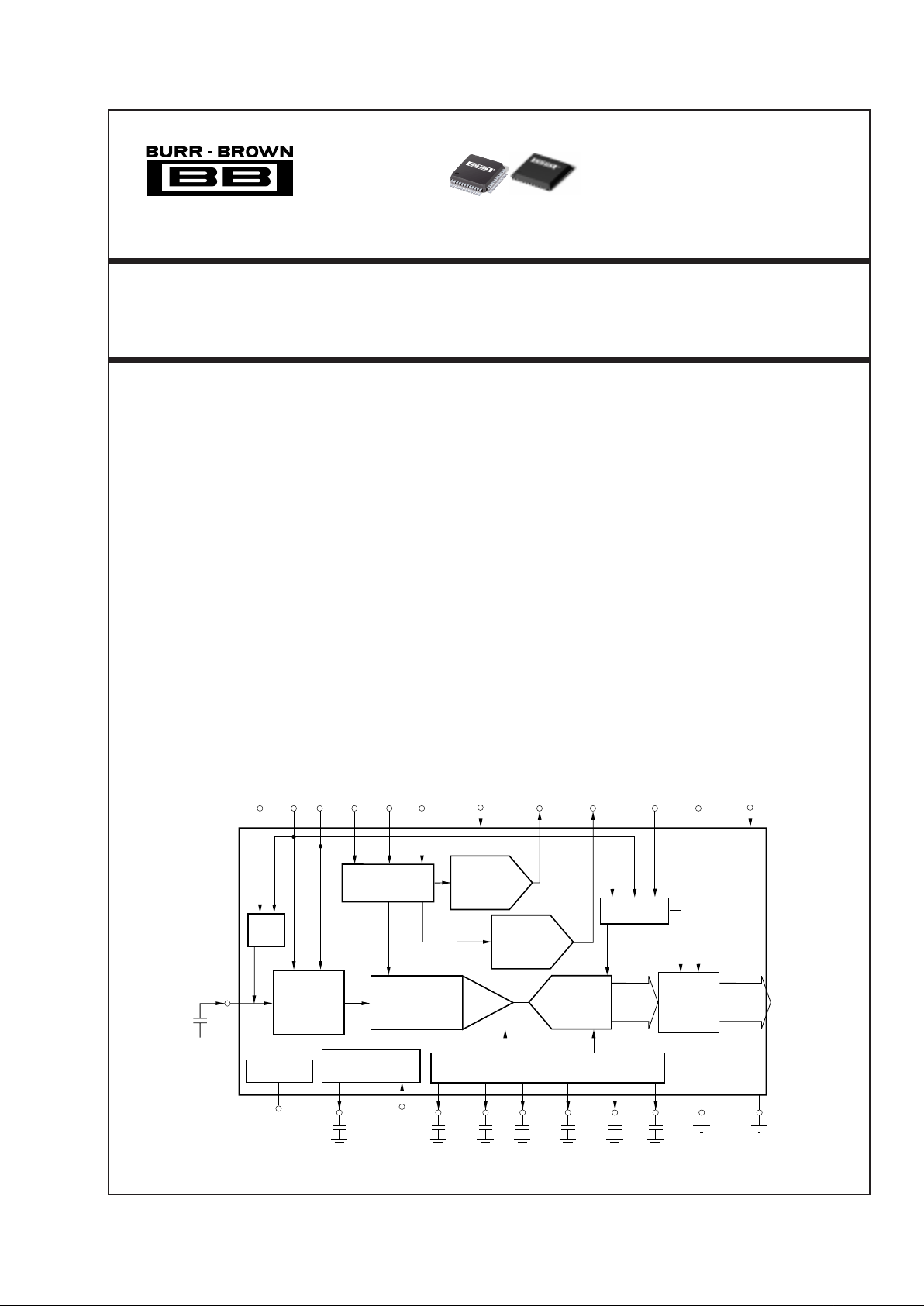
DESCRIPTION
The VSP2212 is a complete mixed-signal processing
IC for digital cameras, providing signal conditioning
and analog-to-digital conversion for the output of a
CCD array. The primary CCD channel provides Correlated Double Sampling (CDS) to extract video information from the pixels, –6dB to +42dB gain ranging
with digital control for varying illumination conditions, and black level clamping for an accurate black
reference. Input signal clamping and offset correction
of the input CDS is also performed. The stable gain
control is linear in dB. Additionally, the black level is
quickly recovered after gain change. The two on-chip
general-purpose 8-bit digital-to-analog converters allow you to obtain analog various control voltage, such
as V
SUB
control of CCD imager. The VSP2212 is the
high-performance version of the VSP2000/2100 families. The VSP2212Y is available in an LQFP-48 package and the VSP2212M is avail able in a VQFN-48
package. Both products operate from a single +3V/
+3.3V supply.
©
2000 Burr-Brown Corporation PDS-1598A Printed in U.S.A. May, 2000
International Airport Industrial Park • Mailing Address: PO Box 11400, Tucson, AZ 85734 • Street Address: 6730 S. Tucson Blvd., Tucson, AZ 85706 • Tel: (520) 746-1111
Twx: 910-952-1111 • Internet: http://www.burr-brown.com/ • Cable: BBRCORP • Telex: 066-6491 • FAX: (520) 889-1510 • Immediate Product Info: (800) 548-6132
For most current data sheet and other product
information, visit www.burr-brown.com
8-Bit
D/A Converter
(DAC0)
8-Bit
D/A Converter
(DAC1)
Programmable
Gain
Amplifier
(PGA)
Input
Clamp
Reference Voltage Generator
Preblanking
Timing
Control
Serial Interface
Output
Latch
Correlated
Double
Sampling
(CDS)
Analog
to
Digital
Converter
12-Bit
Digital
Output
–6dB
to
+42dB
CCDIN
CCD
Output
Signal
PBLK
Optical Black (OB)
Level Clamping
COB
CLPOB
SHPCLPDM SHD SLOAD SCLK SDATA
V
CC
RESET
DACOUT0 DACOUT1 DRV
DD
ADCCK
BYPP2 BYP BYPM REFN CM REFP DRVGND GNDA
B[11:0]
VSP2212
VSP2212
Page 2

2
®
VSP2212
SPECIFICATIONS
At TA = full specified temperature range, VCC = +3.0V, DRVDD = +3.0V, conversion rate (f
ADDCK
) = 20MHz, unless otherwise specified.
VSP2212Y
PARAMETER CONDITIONS MIN TYP MAX UNITS
RESOLUTION 12 Bits
MAXIMUM CONVERSION RATE 20 MHz
DIGITAL INPUT
Logic Family TTL
Input Voltage LOW to HIGH Threshold Voltage (VT+) 1.7 V
HIGH to LOW Threshold Voltage (VT–) 1.0 V
Input Current Logic HIGH (I
IH
), VIN = +3V ±20 µA
Logic LOW (I
IL
), VIN = 0V ±20 µA
ADCCK Clock Duty Cycle 50 %
Input Capacitance 5pF
Maximum Input Voltage –0.3 5.3 V
DIGITAL OUTPUT
Logic Family CMOS
Logic Coding Straight Binary
Output Voltage Logic HIGH (V
OH
), IOH = –2mA 2.4 V
Logic LOW (V
OL
), IOL = 2mA 0.4 V
ANALOG INPUT (CCDIN)
Input Signal Level for Full-Scale Out PGA Gain = 0dB 900 mV
Input Capacitance 15 pF
Input Limit –0.3 3.3 V
TRANSFER CHARACTERISTICS
Differential Non-Linearity (DNL) PGA Gain = 0dB ±0.5 LSB
Integral Non-Linearity (INL) PGA Gain = 0dB ±1 LSB
No Missing Codes Guaranteed
Step Response Settling Time Full-Scale Step Input 1 Pixels
Overload Recovery Time Step Input from 1.8V to 0V 2 Pixels
Data Latency 9 (fixed) Clock Cycles
Signal-to-Noise Ratio
(1)
Grounded Input Cap, PGA Gain = 0dB
79 dB
Grounded Input Cap, Gain = +24dB
55 dB
CCD Offset Correction Range –180 200 mV
CDS
Reference Sample Settling Time Within 1 LSB, Driver Impedance = 50Ω 11 ns
Data Sample Settling Time Within 1 LSB, Driver Impedance = 50Ω 11 ns
INPUT CLAMP
Clamp-On Resistance 400 Ω
Clamp Level 1.5 V
PROGRAMMABLE GAIN AMPLIFIER (PGA)
Gain Control Resolution 10 Bits
Maximum Gain Gain Code = 1111111111 42 dB
High Gain Gain Code = 1101001000 34 dB
Medium Gain Gain Code = 1000100000 20 dB
Low Gain Gain Code = 0010000000 0 dB
Minimum Gain Gain Code = 0000000000 –6 dB
Gain Control Error ±0.5 dB
OPTICAL BLACK CLAMP LOOP
Control DAC Resolution 10 Bits
Optical Black Clamp Level Programmable Range of Clamp Level 2 242 LSB
OBCLP Level at CODE = 1000 130 LSB
Minimum Output Current for Control DAC COB Pin ±0.15 µA
Maximum Output Current for Control DAC COB Pin ±153 µA
Loop Time Constant C
COB
= 0.1µF 40.7 µs
Slew Rate C
COB
= 0.1µF, Output Current 1530 V/s
from Control DAC is Saturated
GENERAL-PURPOSE 8-BIT DAC (DAC0, DAC1)
Minimum Output Voltage Input Code = 00000000 0.1 V
Maximum Output Voltage Input Code = 11111111 2.9 V
Differential Non-Linearity (DNL) At Input Code = 16 to 224 ±0.25 LSB
Integral Non-Linearity (INL) At Input Code = 16 to 192 ±1 LSB
Offset Error ±200 mV
Gain Error ±5%
Monotonicity Guaranteed
NOTE: (1) SNR = 20 log (full-scale voltage/rms noise).
Page 3
3
®
VSP2212
Supply Voltage
(2)
.............................................................................................................. +4.0V
Supply Voltage Differences
(3)
.................................................................................. ±0.1V
Ground Voltage Differences
(4)
................................................................................. ±0.1V
Digital Input Voltage ............................................................ –0.3V to 5.3V
Analog Input Voltage ................................................ –0.3V to V
CC
+ 0.3V
Input Current (any pins except supplies) ....................................... ±10mA
Operating Temperature .................................................. –25°C to +85°C
Storage Temperature ..................................................... –55°C to +125°C
Junction Temperature .................................................................... +150°C
Lead Temperature (soldering, 5s) ................................................. +260°C
Package Temperature (IR reflow, peak, 10s) ............................... +235°C
NOTES: (1) Stresses above those listed under Absolute Maximum Ratings
may cause permanent damage to the device. Exposure to absolute maximum
conditions for extended periods may affect device reliability.
(2) V
CC
, DRVDD. (3) Among VCC. (4) Among GNDA and DRVGND.
ABSOLUTE MAXIMUM RATINGS
(1)
ELECTROSTATIC
DISCHARGE SENSITIVITY
This integrated circuit can be damaged by ESD. Burr-Brown
recommends that all integrated circuits be handled with
appropriate precautions. Failure to observe proper handling
and installation procedures can cause damage.
ESD damage can range from subtle performance degradation to complete device failure. Precision integrated circuits
may be more susceptible to damage because very small
parametric changes could cause the device not to meet its
published specifications.
PACKAGE SPECIFIED
DRAWING TEMPERATURE PACKAGE ORDERING TRANSPORT
PRODUCT PACKAGE NUMBER RANGE MARKING NUMBER
(1)
MEDIA
VSP2212Y LQFP-48 340 –25°C to +85°C VSP2212Y VSP2212Y 250-Piece Tray
"""""VSP2212Y/2K Tape and Reel
VSP2212M VQFN-48 369 –25°C to +85°C VSP2212M VSP2212M 250-Piece Tray
"""""VSP2212Y/2M Tape and Reel
NOTE: (1) Models with a slash (/) are available only in Tape and Reel in the quantities indicated (e.g., /2K indicates 2000 devices per reel). Ordering 2000 pieces
of “VSP2212Y/2K” will get a single 2000-piece Tape and Reel.
PACKAGE/ORDERING INFORMATION
The information provided herein is believed to be reliable; however, BURR-BROWN assumes no responsibility for inaccuracies or omissions. BURR-BROWN
assumes no responsibility for the use of this information, and all use of such information shall be entirely at the user’s own risk. Prices and specifications are subject
to change without notice. No patent rights or licenses to any of the circuits described herein are implied or granted to any third party. BURR-BROWN does not
authorize or warrant any BURR-BROWN product for use in life support devices and/or systems.
REFERENCE
Positive Reference Voltage 1.75 V
Negative Reference Voltage 1.25 V
POWER SUPPLY
Supply Voltage V
CC
, DRV
DD
2.7 3.0 3.6 V
Power Dissipation
Normal Operation Mode
No Load, DAC0 and DAC1 are Suspended
99 mW
Stand-By Mode f
ADDCK
= NOT Apply 6 mW
TEMPERATURE RANGE
Operating Temperature –25 +85 °C
Storage Temperature –55 +125 °C
Thermal Resistance,
θ
JA
LQFP-48 100 °C/W
VSP2212Y
PARAMETER CONDITIONS MIN TYP MAX UNITS
SPECIFICATIONS (Cont.)
At TA = full specified temperature range, VCC = +3.0V, DRVDD = +3.0V, conversion rate (f
ADDCK
) = 20MHz, unless otherwise specified.
PRODUCT ORDERING NUMBER
VSP2212Y DEM-VSP2212Y
DEMO BOARD ORDERING INFORMATION
Page 4
4
®
VSP2212
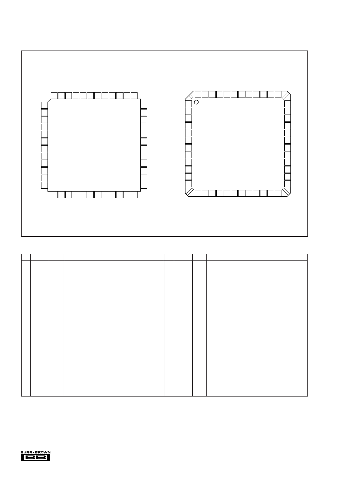
PIN CONFIGURATION
36
35
34
33
32
31
30
29
28
27
26
25
GNDA
GNDA
V
CC
V
CC
BYPM
BYP
CCDIN
BYPP2
COB
V
CC
GNDA
GNDA
SCLK
SDATA
SLOAD
RESET
DACOUT1
DACOUT0
GNDA
GNDA
VCCREFN
REFP
CM
DRV
DD
DRVGND
GNDA
ADCCK
GNDA
V
CC
PBLK
CLPOB
SHP
SHD
CLPDM
V
CC
1
2
3
4
5
6
7
8
9
10
11
12
B0 (LSB)
B1
B2
B3
B4
B5
B6
B7
B8
B9
B10
B11 (MSB)
48 47 46 45 44 43 42
41 40 39 38
13 14 15 16 17 18 19 20 21 22 233724
VSP2212
25 GNDA P Analog Ground
26 GNDA P Analog Ground
27 V
CC
P Analog Power Supply
28 COB AO Optical Black Clamp Loop Reference (Bypass to Ground
(3)
)
29 BYPP2 AO Internal Reference P (Bypass to Ground
(4)
)
30 CCDIN AI CCD Signal Input
31 BYP AO Internal Reference C (Bypass to Ground
(5)
)
32 BYPM AO Internal Reference N (Bypass to Ground
(4)
)
33 V
CC
P Analog Power Supply
34 V
CC
P Analog Power Supply
35 GNDA P Analog Ground
36 GNDA P Analog Ground
37 CM AO
A/D Converter Common-Mode Voltage (Bypass to Ground
(5)
)
38 REFP AO A/D Converter Positive Reference (Bypass to Ground
(5)
)
39 REFN AO A/D Converter Negative Reference (Bypass to Ground
(5)
)
40 V
CC
P Analog Power Supply
41 GNDA P Analog Ground
42 GNDA P Analog Ground
43
DACOUT0
AO General-Purpose 8-Bit D/A Converter
(DAC0) Output Voltage
44
DACOUT1
AO General-Purpose 8-Bit D/A Converter
(DAC1) Output Voltage
45 RESET DI Asynchronous System Reset (Active LOW)
46 SLOAD DI Serial Data Latch Signal (Triggered at the Rising Edge)
47 SDATA DI Serial Data Input
48 SCLK DI Clock for Serial Data Shift (Triggered at the Rising Edge)
PIN NAME TYPE
(1)
DESCRIPTION
1 B0 (LSB) DO Bit 0, A/D Converter Output, Least Significant Bit
2 B1 DO Bit 1, A/D Converter Output
3 B2 DO Bit 2, A/D Converter Output
4 B3 DO Bit 3, A/D Converter Output
5 B4 DO Bit 4, A/D Converter Output
6 B5 DO Bit 5, A/D Converter Output
7 B6 DO Bit 6, A/D Converter Output
8 B7 DO Bit 7, A/D Converter Output
9 B8 DO Bit 8, A/D Converter Output
10 B9 DO Bit 9, A/D Converter Output
11 B10 DO Bit 10, A/D Converter Output
12
B11 (MSB)
DO Bit 11, A/D Converter Output, Most Significant Bit
13 DRV
DD
P Power Supply, Exclusively for Digital Output
14 DRVGND P Digital Ground, Exclusively for Digital Output
15 GNDA P Analog Ground
16 ADCCK DI Clock for Digital Output Buffer
17 GNDA P Analog Ground
18 V
CC
P Analog Power Supply
19 PBLK DI Preblanking:
HIGH = Normal Operation Mode
LOW = Preblanking Mode: Digital Output “All Zero”
20 CLPOB DI Optical Black Clamp Pulse (Default = Active LOW
(2)
)
21 SHP DI
CDS Reference Level Sampling Pulse (Default = Active LOW
(2)
)
22 SHD DI CDS Data Level Sampling Pulse (Default = Active LOW
(2)
)
23 CLPDM DI Dummy Pixel Clamp Pulse (Default = Active LOW
(2)
)
24 V
CC
P Analog Power Supply
PIN NAME
TYPE
(1)
DESCRIPTION
PIN DESCRIPTIONS
NOTES: (1) Type designators: P = Power Supply and Ground; DI = Digital Input; DO = Digital Output; AI = Analog Input; AO = Analog Output. (2) Refer to the “Serial
Interface” section for more detail. (3) Should be connected to ground with a bypass capacitor. We recommend the value of 0.1µF to 0.22 µF, however, it depends
on the application environment. Refer to the “Optical Black Level Clamp Loop” section for more detail. (4) Should be connected to ground with a bypass capacitor.
We recommend the value of 1000pF, however, it depends on the application environment. Refer to the “Voltage Reference” section for more detail. (5) Should be
connected to ground with a bypass capacitor (0.1µF). Refer to the “Voltage Reference” section for more detail.
36
35
34
33
32
31
30
29
28
27
26
25
GNDA
GNDA
V
CC
V
CC
BYPM
BYP
CCDIN
BYPP2
COB
V
CC
GNDA
GNDA
SCLK
SDATA
SLOAD
RESET
DACOUT1
DACOUT0
GNDA
GNDA
VCCREFN
REFP
CM
DRV
DD
DRVGND
GNDA
ADCCK
GNDA
V
CC
PBLK
CLPOB
SHP
SHD
CLPDM
V
CC
1
2
3
4
5
6
7
8
9
10
11
12
B0 (LSB)
B1
B2
B3
B4
B5
B6
B7
B8
B9
B10
B11 (MSB)
48 47 46 45 44 43 42
41 40 39 38
13 14 15 16 17 18 19 20 21 22 233724
VSP2212M
Top View LQFP Top View VQFN
Page 5

5
®
VSP2212
CDS TIMING SPECIFICATIONS
N
N – 9 N – 8 N – 7N – 11 N – 10
CCD
Output
Signal
SHP
(1)
SHD
(1)
ADCCK
B0 to B11
t
WP
N + 1 N + 2 N + 3
t
DP
t
OD
t
HOLD
t
ADC
t
INHIBIT
t
ADC
t
CKP
t
CKP
t
CKP
t
S
t
WD
t
PD
t
S
SYMBOL PARAMETER MIN TYP MAX UNITS
t
CKP
Clock Period 48 ns
t
ADC
ADCCK HIGH/LOW Pulse Width 20 ns
t
WP
SHP Pulse Width 14 ns
t
WD
SHD Pulse Width 11 ns
t
PD
SHP Trailing Edge to SHD Leading Edge
(1)
8ns
t
DP
SHD Trailing Edge to SHP Leading Edge
(1)
12 ns
t
S
Sampling Delay 5 ns
t
INHIBIT
Inhibited Clock Period 20 ns
t
HOLD
Output Hold Time 7 ns
t
OD
Output Delay (No Load) 38 ns
DL Data Latency, Normal Operation Mode 9 (fixed) Clock Cycles
NOTE: (1) The description and timing diagrams in this data sheet are all based on the polarity of Active LOW
(default value). The active polarity (Active LOW or Active HIGH) can be chosen through the serial interface.
Refer to the “Serial Interface” section for more detail.
Page 6

6
®
VSP2212
SERIAL INTERFACE TIMING SPECIFICATIONS
SYMBOL PARAMETER MIN TYP MAX UNITS
t
CKP
Clock Period 100 ns
t
CKH
Clock HIGH Pulse Width 40 ns
t
CKL
Clcok LOW Pulse Width 40 ns
t
DS
Data Setup Time 30 ns
t
DH
Data Hold TIme 30 ns
t
XS
SLOAD to SCLK Setup Time 30 ns
t
XH
SCLK to SLOAD Setup Time
(1)
30 ns
NOTES: (1) It is effective for the data shift operation at the rising edge of SCLK during SLOAD is LOW period.
And Input 2 bytes data are loaded to the parallel latch in the VSP2212 at the rising edge of SLOAD. (2) When
the input serial data is longer than 2 bytes (16 bits), the last 2 bytes become effective and the former bits are
discarded.
SLOAD
SCLK
(1)
MSB
LSB
SDATA
t
CKP
t
XS
t
CKH
t
DH
t
DS
2 Bytes
(2)
t
CKL
t
XH
Page 7

7
®
VSP2212
THEORY OF OPERATION
INTRODUCTION
The VSP2212 is a complete mixed-signal IC that contains
all of the key features associated with the processing of the
CCD imager output signal in a video camera, a digital still
camera, security camera, or similar applications. A simplified block diagram is shown in the front page of this data
sheet. The VSP2212 includes a correlated double sampler
(CDS), programmable gain amplifier (PGA), Analog-toDigital Converter (ADC), input clamp, optical black (OB)
level clamp loop, serial interface, timing control, reference
voltage generator, and general purpose 8-bit Digital-toAnalog Converters (DAC). We recommend an off-chip
emitter follower buffer between the CCD output and the
VSP2212 CCDIN input. The PGA gain control, clock polarity setting, and operation mode selection can be made
through the serial interface. All parameters are reset to the
default value when the RESET pin goes to LOW asynchronously from the clocks.
CORRELATED DOUBLE SAMPLER (CDS)
The output signal of a CCD imager is sampled twice during
one pixel period: one at the reference interval and the other
at the data interval. Subtracting these two samples extracts
the video information of the pixel as well as removes any
noise that is common, or correlated, to both the intervals.
Therefore, the CDS is very important to reduce the reset
noise and the low-frequency noises that are present on the
CCD output signal. Figure 1 shows the simplified block
diagram of the CDS and input clamp.
A 0.1µF capacitor is recommended for CIN, depending on
the application environment. Additionally, we recommend
an off-chip emitter follower buffer that can drive more than
10pF, because 10pF of the sampling capacitor and a few pF
of stray capacitance can be seen at the input pin. The analog
input signal range at the CCDIN pin is 1Vp-p, and the
appropriate common mode voltage for the CDS is around
0.5V to 1.5V.
The reference level is sampled during SHP active period,
and the voltage level is held on sampling capacitor C1 at the
trailing edge of SHP. The data level is sampled during SHD
active period, and the voltage level is held on the sampling
capacitor C2 at the trailing edge of SHD. The switchedcapacitor amplifier then performs the subtraction of these
two levels.
The active polarity of SHP/SHD (Active HIGH or Active
LOW) can be selected through the serial interface (refer to
“Serial Interface” section for more detail). The default value
of SHP/SHD is “Active LOW”. However, immediately after
power on, this value is “Unknown”. For this reason, the
appropriate value must be set by using the serial interface, or
reset to the default value by the RESET pin. The description
and the timing diagrams in this data sheet are all based on
the polarity of Active LOW (default value).
INPUT CLAMP OR DUMMY PIXEL CLAMP
The buffered CCD output is capacitively coupled to the
VSP2212. The purpose of the input clamp is to restore the
DC component of the input signal that was lost with the AC
coupling and establish the desired DC bias point for the
CDS. Figure 1 also shows a simplified block diagram of the
input clamp. The input level is clamped to internal reference
voltage CM (1.5V) during the dummy pixel interval. More
specifically, when both CLPDM and SHP are active, the
dummy clamp function becomes active. If the dummy pixels
and/or the CLPDM pulse are not available in your system,
the CLPOB pulse can be used in place of CLPDM, as long
as the clamping takes place during black pixels. In this case,
both the CPLDM pin (actives as same timing as CLPOB)
and SHP become active during the optical black pixel
interval, and then the dummy clamp function becomes
active.
The active polarity of CLPDM and SHP (Active HIGH or
Active LOW) can be selected through the serial interface
(refer to the “Serial Interface” section for more detail).
The default value of CLPDM and SHP is “Active LOW”.
However, immediately after power on, this value is “Unknown”. For this reason, the appropriate value must be set
by using the serial interface, or reset to the default value by
the RESET pin. The description and the timing diagrams in
this data sheet are all based on the polarity of Active LOW
(default value).
FIGURE 1. Simplified Block Diagram of CDS and Input
Clamp.
OPA
C
IN
C
1
10pF
C
2
10pF
CM (1.5V)
CCDIN
SHP
SHD
CCD
Output
SHP
CLPDM
VSP2212
The CDS is driven through an off-chip coupling capacitor
(CIN). AC coupling is strongly recommended because the
DC level of the CCD output signal is usually several volts
too high for the CDS to work properly.
Page 8

8
®
VSP2212
HIGH PERFORMANCE ANALOG-TO-DIGITAL
CONVERTER (ADC)
The Analog-to-Digital Converter (ADC) utilizes a fully
differential and pipelined architecture. This ADC is well
suited for low-voltage operations, low-power consumption
requirements, and high-speed applications. It guarantees
12-bit resolution of output data with no missing code.
The VSP2212 includes a reference voltage generator for the
ADC. REFP (Positive Reference, pin 38), REFN (Negative
Reference, pin 39), and CM (Common-Mode Voltage,
pin 37) should be bypassed to ground with a 0.1µF ceramic
capacitor, and should not be used elsewhere in the system;
they affect the stability of these reference levels, and cause
ADC performance degradation. Note that these are analog
output pins.
PROGRAMMABLE GAIN AMPLIFIER (PGA)
Figure 2 shows the characteristics of the PGA gain. The
PGA provides a gain range of –6dB to +42dB, which is
linear in dB. The gain is controlled by a digital code with
10-bit resolution, and can be set through the serial interface
(refer to the “Serial Interface” section for more detail).
The default value of the gain control code is 128 (PGA
Gain = 0dB). However, immediately after power on, this
value is “Unknown”. For this reason, the appropriate value
must be set by using the serial interface, or reset to the
default value by the RESET pin.
OPTICAL BLACK (OB) LEVEL CLAMP LOOP
During the effective pixel interval, the reference level of the
CCD output signal is clamped to the OB level by the OB
level clamp loop. To determine the loop time constant, an
off-chip capacitor is required, and should be connected to
COB (pin 28). Time constant T is given in the following
equation:
T = C/(16384 • I
min
)
Where C is the capacitor value connected to COB, I
min
is the
minimum current (0.15µA) of the control DAC in the OB
level clamp loop, and 0.15µA is equivalent to 1LSB of the
DAC output current. When C is 0.1µF, the time constant T
is 40.7µs.
Additionally, the slew rate SR is given the following equation:
SR = I
max
/C
Where C is the capacitor value connected to COB, I
max
is the
maximum current (153µA) of the control DAC in the OB
level clamp loop, and 153µA is equivalent to 1023LSB of
the DAC output current.
Generally, OB level clampling at high speed causes “Clamp
Noise” (or “White Streak Noise”), however, the noise will
decrease by increasing C. On the other hand, an increased C
requires a much longer time to restore from Stand-By mode,
or right after power on. Therefore, we consider 0.1µF to
0.22µF a reasonable value for C. However, it depends on the
application environment; we recommend making careful
adjustments using trial-and-error.
The “OB clamp level” (the pedestal level) is programmable
through the serial interface (refer to the “Serial Interface”
section for more detail). Table I shows the relationship
between input code and the OB clamp level.
To extract the video information correctly, the CCD signal
must be referenced to a well-established Optical Black (OB)
level. The VSP2212 has an auto-calibration loop to establish
the OB level using the optical black pixels output from the
CCD imager. The input signal level of the OB pixels is
identified as the real “OB level”, and the loop should be
closed during this period while CLPOB is active.
FIGURE 2. Characteristics of PGA Gain.
Input Code for Gain Control (0 to 1023)
Gain (dB)
50
40
30
20
10
0
–10
0
100
200
300
400
500
600
700
800
900
1k
1023
INPUT CODE OB CLAMP LEVEL, LSBs OF 12 BITS
0000 2 LSB
0001 18 LSB
0010 34 LSB
0011 50 LSB
0100 66 LSB
0101 82 LSB
0110 98 LSB
0111 114 LSB
1000 (Default) 130 LSB
1001 146 LSB
1010 162 LSB
1011 178 LSB
1100 194 LSB
1101 210 LSB
1110 226 LSB
1111 242 LSB
TABLE I. Programmable OB Clamp Level.
Page 9

9
®
VSP2212
The active polarity of CLPOB (Active HIGH or Active
LOW) can be selected through the serial interface (refer to
the “Serial Interface” section for more detail). The default
value of CLPOB is “Active LOW”. However, immediately
after power on, this value is “Unknown”. For this reason, the
appropriate value must be set by using serial interface, or
reset to the default value by the RESET pin. The description
and the timing diagrams in this data sheet are all based on
the polarity of Active LOW (default value).
PREBLANKING AND DATA LATENCY
Some CCDs have large transient output signals during
blanking intervals. Such signals may exceed the VSP2212’s
1Vp-p input signal range and would overdrive the VSP2212
into saturation. Recovery time from the saturation could be
substantial. To avoid this, the VSP2212 has an input blanking (or preblanking) function (PBLK). When PBLK goes to
LOW, the CCDIN input is disconnected from the internal
CDS stage and large transients are prevented from passing
through. The VSP2212’s digital outputs will go to all ZEROs
at the 11th rising edge of ADCCK, from just after PBLK sets
to LOW, to accommodate the clock latency of the VSP2212.
In this mode, the digital output data come out at the rising
edge of ADCCK with a delay of 11 clock cycles (data
latency is 11). Note that in the normal operation mode, the
digital output data come out at the rising edge of ADCCK
with a delay of 9 clock cycles (data latency is 9).
It is recommended that CLPOB should not be activated
during PBLK active period in order to keep a stable and
accurate OB clamp level. Since the CCDIN input is disconnected from the internal circuit, even if the auto-calibration
loop is closed while CLPOB is active, the OB clamp level is
different from the “actual” OB level established by CCD
imager output. The missed OB clamp level would affect the
picture quality.
If the input voltage is higher than the supply rail by 0.3V, or
lower than the ground rail by 0.3V, protection diodes will be
turned on to prevent the input voltage from going further.
Such a high swing signal may cause device damage to the
VSP2212 and should be avoided.
STAND-BY MODE
For the purpose of power saving, the VSP2212 can be set to
Stand-By mode (or Power-Down mode) through the serial
interface when the VSP2212 is not in use. Refer to “Serial
Interface” section for more detail. In this mode, all the
function blocks are disabled and the digital outputs will go
to all ZEROs. The consumption current will drop to 1mA.
Since all the bypass capacitors will discharge during this
mode, a substantial time (usually of the order of 200ms to
300ms) is required to power up from Stand-By mode.
VOLTAGE REFERENCE
All the reference voltages and bias currents needed in the
VSP2212 are generated by its internal bandgap circuitry.
The CDS and the ADC use mainly three reference voltages:
REFP (Positive Reference, pin 38), REFN (Negative Reference, Pin 39) and CM (Common-Mode Voltage, pin 37).
REFP, REFN and CM should be heavily decoupled with
appropriate capacitors (e.g., 0.1µF ceramic capacitor), and
should not be used elsewhere in the system; they affect the
stability of the reference level, and cause ADC performance
degradation. Note that these are analog output pins.
BYPP2 (pin 29), BYP(pin 31), BYPM(pin 32) are also
reference voltages to be used in the analog circuit. BYP
should be connected to ground with 0.1µF ceramic capacitor. The capacitor value for BYPP2 and BYPM affects the
step response. Therefore, we consider 1000pF is the reasonable value. However, it depends on the application environment; we recommend making careful adjustments using
trial-and-error.
All of BYPP2, BYP and BYPM should be heavily decoupled
with appropriate capacitors, and not used elsewhere in the
system. They affect the stability of these reference level, and
cause performance degradation. Note that these are analog
output pins.
SERIAL INTERFACE
The serial interface has a 2-byte shift register and various
parallel registers to control all the digitally programmable
features of the VSP2212. Writing to these registers is controlled by four signals (SLOAD, SCLK, SDATA, RESET).
To enable the shift register, SLOAD must be pulled LOW.
SDATA is the serial data input and the SCLK is the shift
clock. The data at SDATA is taken into the shift register at
the rising edge of SCLK. The data length should be 2 bytes.
After the 2-byte shift operation, the data in the shift register
is transferred to the parallel latch at the rising edge of
SLOAD. In addition to the parallel latch, there are several
registers dedicated to the specific features of the device and
they are synchronized with ADCCK. It takes 5 or 6 clock
cycles for the data in the parallel latch to be written to those
registers. Therefore, to complete the data updates, it requires
5 or 6 clock cycles after the parallel latching by the rising
edge of SLOAD.
See Table II for the serial interface data format. TEST is the
flag for the test mode (Burr-Brown proprietary only), A0 to
A2 is the address for the various registers, and D0 to D11 is
the data or the operand field.
Page 10

10
®
VSP2212
REGISTER DEFINITIONS
C[2:0] Operation Mode, Normal/Stand-By
Serial Interface and Registers are always active, independently from the operation mode.
C0 = Operation Mode for the entire chip except DAC0/DAC1
(C0 = 0 “Active”; C0 = 1 “Stand-by”)
C1 = for DAC0 (C0 = 0 “Active”; C0 = 1 “Stand-by”)
C2 = for DAC1 (C0 = 0 “Active”; C0 = 1 “Stand-by”)
G[9:0] The Characteristics of PGA Gain (refer to Figure 2)
O[3:0] Programmable OB Clamp Level (refer to Table I)
P[2:0] Clock Polarity
P0 = Polarity for CLPDM (P0 = 0 “Active LOW”; P0 = 1 “Active HIGH”)
P1 = for CLPOB (P0 = 0 “Active LOW”; P0 = 1 “Active HIGH”)
P2 = for SHP/SHD (P0 = 0 “Active LOW”; P0 = 1 “Active HIGH”)
E[7:0] DAC0 Data (All ZEROs = Output Voltage Minimum; All ONEs = Output Voltage Maximum)
F[7:0] DAC1 Data (All ZEROs = Output Voltage Minimum; All ONEs = Output Voltage Maximum)
Immediately after power on, these values are “Unknown”. The appropriate value must be set by using the serial interface, or
reset to the default value by the RESET pin.
Default values are:
C[2:0] = 000 Normal Operation Mode
G[9:0] = 0010000000 PGA Gain = 0dB
O[3:0] = 1000 OB Clamp Level = 130LSB
P[2:0] = 000 CLPDM, CLPOB, SHP/SHD are all “Active LOW”
(1)
E[7:0] = 00000000 DAC0 Output Voltage = Minimum
F[7:0] = 00000000 DAC1 Output Voltage = Minimum
NOTE: (1) The description and the timing diagrams in this data sheet are all based on the polarity of Active LOW (default value).
REGISTERS TEST A2 A1 A0 D11 D10 D9 D8 D7 D6 D5 D4 D3 D2 D1 D0
Configuration 0 0 0 0 0 0 0 0 0 0 0 0 0 C2 C1 C0
PGA Gain 0 0 0 1 0 0 G9 G8 G7 G6 G5 G4 G3 G2 G1 G0
OB Clamp Level 0 0 1 0 0 0 0 0 0 0 0 0 O3 O2 O1 O0
Clock Polarity 0 0 1 1 0 0 0 0 0 0 0 0 0 P2 P1 P0
DAC0 Data 0 1 0 0 0 0 0 0 E7 E6 E5 E4 E3 E2 E1 E0
DAC1 Data 0 1 0 1 0 0 0 0 F7 F6 F5 F4 F3 F2 F1 F0
Reserved 0 1 1 0 x x x x x x x x x x x x
Reserved 1 x x x x x x x x x x x x x x x
x = Don’t Care.
TABLE II. Serial Interface Data Format.
Page 11

11
®
VSP2212
TIMINGS
The CDS and the ADC are operated by SHP/SHD and their
derivative timing clocks generated by the on-chip timing
generator. The digital output data is synchronized with
ADCCK. The timing relationship among the CCD signal,
SHP/SHD, ADCCK and the output data is shown in the
VSP2212 “CDS Timing Specifications”. CLPOB is used to
activate the black level clamp loop during the OB pixel
interval, and CLPDM is used to activate the input clamping
during the dummy pixel interval. If the CLPDM pulse is not
available in your system, the CLPOB pulse can be used in
place of CLPDM as long as the clamping takes place during
black pixels (refer to the “Input Clamp and Dummy Pixel
Clamp” section for more detail). The clock polarities of
SHP/SHD, CLPOB and CLPDM can be independently set
through the serial interface (refer to the “Serial Interface”
section for more detail). The description and the timing
diagrams in this data sheet are all based on the polarity of
Active LOW (default value). In order to keep a stable and
accurate OB clamp level, we recommend CLPOB should
not be activated during PBLK active period. Refer to the
“Preblanking and Data Latency” section for more detail. In
Stand-By mode, all of ADCCK, SHP, SHD, CLPOB and
CLPDM are internally masked and pulled HIGH.
GENERAL-PURPOSE 8-BIT DIGITAL-TO-ANALOG
CONVERTER (DAC0,DAC1)
The VSP2212 incorporates two identical 8-bit Digital-toAnalog converters (DACs). These DACs are for user-definable options such as iris control and sub-bias voltage control
of the CCD imager. The input data for these DACs is set by
the written data through the serial interface (refer to the
“Serial Interface” section for more detail). DAC input data
that is all ZEROs corresponds to a minimum output voltage
of 0.1V. In a similar manner, all ONEs correspond to a
maximum output voltage of 2.9V. Figure 3 shows the
characteristics.
POWER SUPPLY, GROUNDING AND DEVICE
DECOUPLING RECOMMENDATIONS
The VSP2212 incorporates a very high-precision and highspeed Analog-to-Digital converter and analog circuitry that
are vulnerable to any extraneous noise from the rails or
elsewhere. For this reason, it should be treated as an analog
component and all supply pins except for DRVDD should be
powered by the only analog supply of the system. This will
ensure the most consistent results, since digital power lines
often carry high level of wide band noise that would otherwise be coupled into the device and degrade the achievable
performance. Proper grounding, short lead length and the
use of ground planes are also very important for highfrequency designs. Multi-layer PC boards are recommended
for the best performance, since they offer distinct advantages like minimizing ground impedance, separation of signal layers by ground layers, etc. It is highly recommended
that analog and digital ground pins of the VSP2212 be joined
together at the IC and be connected only to the analog
ground of the system. The driver stage of the digital outputs
(B[11:0]) is supplied through a dedicated supply pin (DRVDD)
and it should be separated from the other supply pins
completely, or at least with a ferrite bead. It is also recommended to keep the capacitive loading on the output data
lines as low as possible (typically less than 15pF). Larger
capacitive loads demand higher charging current surges that
can feed back into the analog portion of the VSP2212 and
affect the performance. If possible, external buffers or latches
should be used, providing the added benefit of isolating the
VSP2212 from any digital noise activities on the data lines.
In addition, resistors in series with each data line may help
minimizing the surge current. Values in the range of 100Ω
to 200Ω will limit the instantaneous current the output stage
has to provide for recharging the parasitic capacitances as
the output levels change from LOW to HIGH, or HIGH to
LOW. Due to high operation speed, the converter also
generates high-frequency current transients and noises that
are fed back into the supply and reference lines. This
requires the supply and reference pins be sufficiently bypassed. In most cases, 0.1µF ceramic chip capacitors are
adequate to decouple the reference pins. Supply pins should
be decoupled to the ground plane with a parallel combination of tantalum (1µF to 22µF) and ceramic (0.1µF) capacitors. The effectiveness of the decoupling largely depends on
the proximity to the individual pin. DRVDD should be
decoupled to the proximity of DRVGND. Special attention
must be paid to the bypassing of COB, BYPP2 and BYPM,
since these capacitor values determine important analog
performances of the device.
Input Control Code (0 to 255)
Output Voltage (V)
3.0
2.5
2.0
1.5
1.0
0.5
0
0
50
100
150
200
250
255
FIGURE 3. Characteristics for general-purpose 8-bit DAC
(DAC0, DAC1).
 Loading...