

Page 1
®
VSP2080
CCD SIGNAL FRONT-END
PROCESSOR FOR DIGITAL CAMERAS
FEATURES
● CCD SIGNAL PROCESSING
Correlated Double Sampling
Black Level Clamping
0 to +34dB Gain Range
55dB SNR Referred to Full Scale
● SELECTABLE LOGIC-INPUT POLARITY
Positive Active or Negative Active
● PORTABLE OPERATION
Low Voltage: 2.7V to 3.6V
Low Power: 144mW at 3.0V
Power-Down Mode: 10mW
DESCRIPTION
The VSP2080 is a complete front-end processing IC
for digital cameras. The VSP2080 provides signal
conditioning for the output of a CCD array. The
VSP2080 provides correlated double sampling to extract the video information from the pixels, 0dB to
+34dB gain range with analog control for varying
illumination conditions, and black level clamping for
an accurate black reference. The stable gain control is
linear in dB. Additionally, the black level quickly
recovers after screen changes. The MODE pin allows
the selection of logic-input polarity. The VSP2080 is
available in a 20-lead TSSOP package.
©
1998 Burr-Brown Corporation PDS-1498B Printed in U.S.A. August, 1999
TM
International Airport Industrial Park • Mailing Address: PO Box 11400, Tucson, AZ 85734 • Street Address: 6730 S. Tucson Blvd., Tucson, AZ 85706 • Tel: (520) 746-1111
Twx: 910-952-1111 • Internet: http://www.burr-brown.com/ • Cable: BBRCORP • Telex: 066-6491 • FAX: (520) 889-1510 • Immediate Product Info: (800) 548-6132
APPLICATIONS
● VIDEO CAMERAS
● DIGITAL STILL CAMERAS
● PC CAMERAS
● SECURITY CAMERAS
CCD R
CCD D
CCD
OUT
Optical
Black Level
Auto-Zero
Dummy
Pixel
Auto-Zero
+28dB
Log
VCA
Correlated
Double
Sampling
Clamp
+6dB
REFCK DATCK
AGC IN
C
DUMC
Internal
Bias
Generator
REFT REFB REF IN
Logic Input
Polarity
Control
MODE
OB
OUT
®
VSP2080
Page 2
®
2
VSP2080
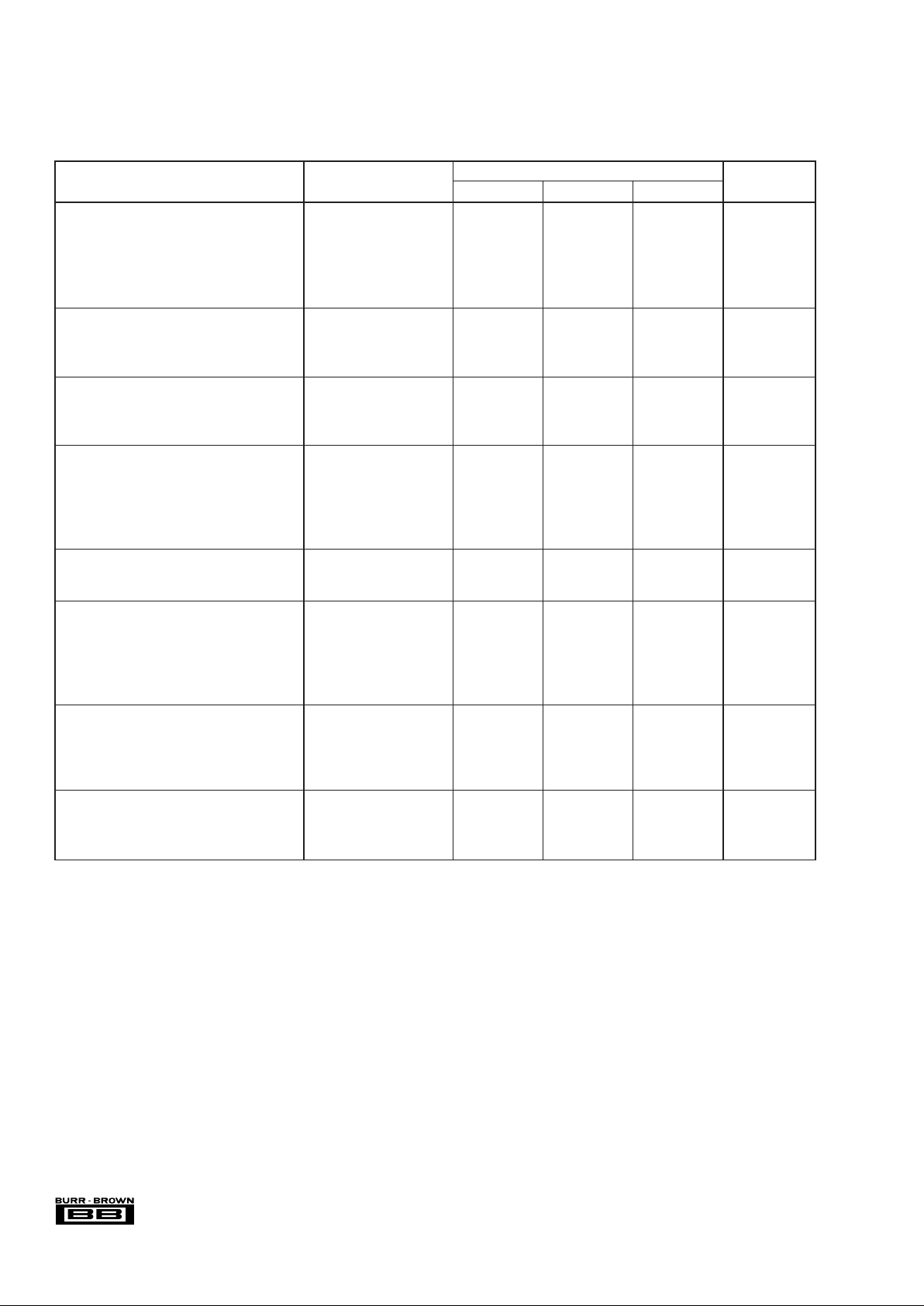
SPECIFICATIONS
At TA = +25°C, and V
DDA
= +3.0V, unless otherwise specified.
VSP2080T
PARAMETER CONDITIONS MIN TYP MAX UNITS
DIGITAL INPUT
Logic Family CMOS
Logic Levels Logic HI 2.5 +V
DDA
V
Logic LO 0 +0.4 V
Logic Currents Logic HI, V
IN
= +V
DDA
10 µA
Logic LO, VIN = 0V 10 µA
ANALOG OUTPUT
Output Voltage 1.0 2.0 V
Output Black Level 1.010 1.030 1.045 x REF IN
Reference Input (REF IN) 0.90 1.0 1.1 V
TRANSFER CHARACTERISTICS
Signal-to-Noise Ratio
(1)
Grounded Input Cap, 55 dB
Gain Min
Black Clamp Level 31 mV
CDS
Data Settling Time to ±0.1% for FS Change From Leading Edge 11 ns
with R
S
= 40 of DATCK
Input Capacitance DATCK LOW 20 pF
Input Time Constant 300 ps
Full-Scale Input Voltage After AC-Coupling Cap 600 mV
INPUT CLAMP
Clamp-On Resistance 3.3 kΩ
Clamp Level 1V
GAIN CONTROL CHARACTERISTICS
Linear Gain Control Voltage Range 0.7 2.3 V
Gain at Max Control Voltage 34 dB
Gain Control Linearity ±1.0 dB
Gain Control Settling Time 10 µs
Transfer Function Linear Range 20.6 dB /V
POWER SUPPLY
Rated Voltage +2.7 +3.0 +3.6 V
Current, Quiescent 48 mA
Power Dissipation 144 mW
Power-Down Mode 10 mW
TEMPERATURE RANGE
Specified Range Ambient –25 +85 °C
Thermal Resistance,
θ
JA
20-Lead TSSOP 130 °C/W
NOTE: (1) SNR = 20log (full-scale voltage / r ms noise).
The information provided herein is believed to be reliable; however, BURR-BROWN assumes no responsibility for inaccuracies or omissions. BURR-BROWN
assumes no responsibility for the use of this information, and all use of such information shall be entirely at the user’s own risk. Prices and specifications are subject
to change without notice. No patent rights or licenses to any of the circuits described herein are implied or granted to any third party. BURR-BROWN does not
authorize or warrant any BURR-BROWN product for use in life support devices and/or systems.
Page 3
®
3
VSP2080
+VS....................................................................................................... +6V
Analog Input.......................................................... –0.3V to (+V
DDA
+0.3V)
Logic Input ............................................................ –0.3V to (+V
DDA
+0.3V)
Case Temperature ......................................................................... +100°C
Junction Temperature .................................................................... +150°C
Storage Temperature..................................................................... +150°C
ABSOLUTE MAXIMUM RATINGS
PIN DESIGNATOR TYPE DESCRIPTION
1 LCM Bypass Attenuator Common-Mode Bypass,
Bypass to GND with 0.1µF capacitor
2 2.4V Bypass Attenuator Ladder Bypass,
Bypass to GND with 0.1µF capacitor
3 OUT Analog Output Analog Output
4 C Capacitor Capacitor for Optical Black Auto-Zero
Loop
5 MODE Logic Input Mode Control for Logic Input:
LO = Positive Pulse Active
HI = Negative Pulse Active
6 OB Logic Input Optical Black Clamp Pulse
7 REFCK Logic Input Sampling Pulse for Reset
8 DATCK Logic Input Sampling Pulse for Data
9 DUMC Logic Input Dummy Pixel Clamp Pulse
10 PD Logic Input Power-Down Control:
LO = Normal Operation
HI = Reduced Power
11 V
DDA
Power Supply Positive Power Supply
12 GND
A
Ground Analog Ground
13 CCD D Analog Input CCD Signal Input
14 CCD R Capacitor Capacitor for Dummy Feedback Loop
15 GND
A
Ground Analog Ground
16 AGC IN Analog Input Sets Gain of Gain Control Amp.
17 V
DDA
Power Supply Positive Power Supply
18 REFT Bypass Bypass for Internal Top Reference
19 REFB Bypass Bypass for Internal Bottom Reference
20 REF IN Analog Input External Reference Input (1.0V)
PIN CONFIGURATION
PIN DESCRIPTIONS
Top View TSSOP
LCM
2.4V
OUT
C
MODE
OB
REFCK
DATCK
DUMC
PD
REF IN
REFB
REFT
V
DDA
AGC IN
GND
A
CCD R
CCD D
GND
A
V
DDA
1
2
3
4
5
6
7
8
9
10
20
19
18
17
16
15
14
13
12
11
VSP2080T
PACKAGE SPECIFIED
DRAWING TEMPERATURE PACKAGE ORDERING TRANSPORT
PRODUCT PACKAGE NUMBER
(1)
RANGE MARKING NUMBER
(2)
MEDIA
VSP2080T 20-Lead TSSOP 353 –25°C to +85°C VSP2080T VSP2080T 250-Piece Tray
" " " " " VSP2080T/2K Tape and Reel
NOTES: (1) For detailed drawing and dimension table, please see end of data sheet, or Appendix C of Burr-Brown IC Data Book. (2) Models with a slash (/ ) are
available only in Tape and Reel in the quantities indicated (e.g., /2K indicates 2000 devices per reel). Ordering 2000 pieces of “VSP2080T/2K” will get a single 2000piece Tape and Reel.
PACKAGE/ORDERING INFORMATION
ELECTROSTATIC
DISCHARGE SENSITIVITY
This integrated circuit can be damaged by ESD. Burr-Brown
recommends that all integrated circuits be handled with
appropriate precautions. Failure to observe proper handling
and installation procedures can cause damage.
ESD damage can range from subtle performance degradation
to complete device failure. Precision integrated circuits may
be more susceptible to damage because very small parametric
changes could cause the device not to meet its published
specifications.
Page 4

®
4
VSP2080
TYPICAL PERFORMANCE CURVES
At TA = +25°C, VDD = +3.0V, and conversion rate = 18MHz, unless otherwise specified.
TIMING DIAGRAM
SYMBOL PARAMETER MIN TYP MAX UNITS
t
0
REFCK Pulse Width 11 14 ns
t
1
REFCK Sampling Delay 1.5 2 ns
t
2
DATCK Pulse Width 11 14 ns
t
3
DATCK Sampling Delay 1.5 2 ns
t
4
Analog Output Settling Time
(1)
110 ns
NOTE: (1) C
LOAD
= 5pF.
CDS Input
(CCD Output)
REFCK
(Pin 7)
DATCK
(Pin 8)
ANALOG OUTPUT
2.0V
1.03V
t
0
t
1
t
2
t
4
t
3
Feedthrough Data Output Interval
N
N + 1 N + 2
27MHz
(Pin 3)
60
50
40
30
20
10
0
Quiescent Current (mA)
QUIESCENT CURRENT vs POWER SUPPLY
2.7 3.0
Power Supply Voltage (V)
3.3
40
35
30
25
20
15
10
5
0
–5
–10
Gain (dB)
GAIN CONTROL CHARACTERISTICS
0.0 0.5 1.0 1.5
AGC
IN
Input (V)
2.0 2.5 3.0
Page 5

®
5
VSP2080
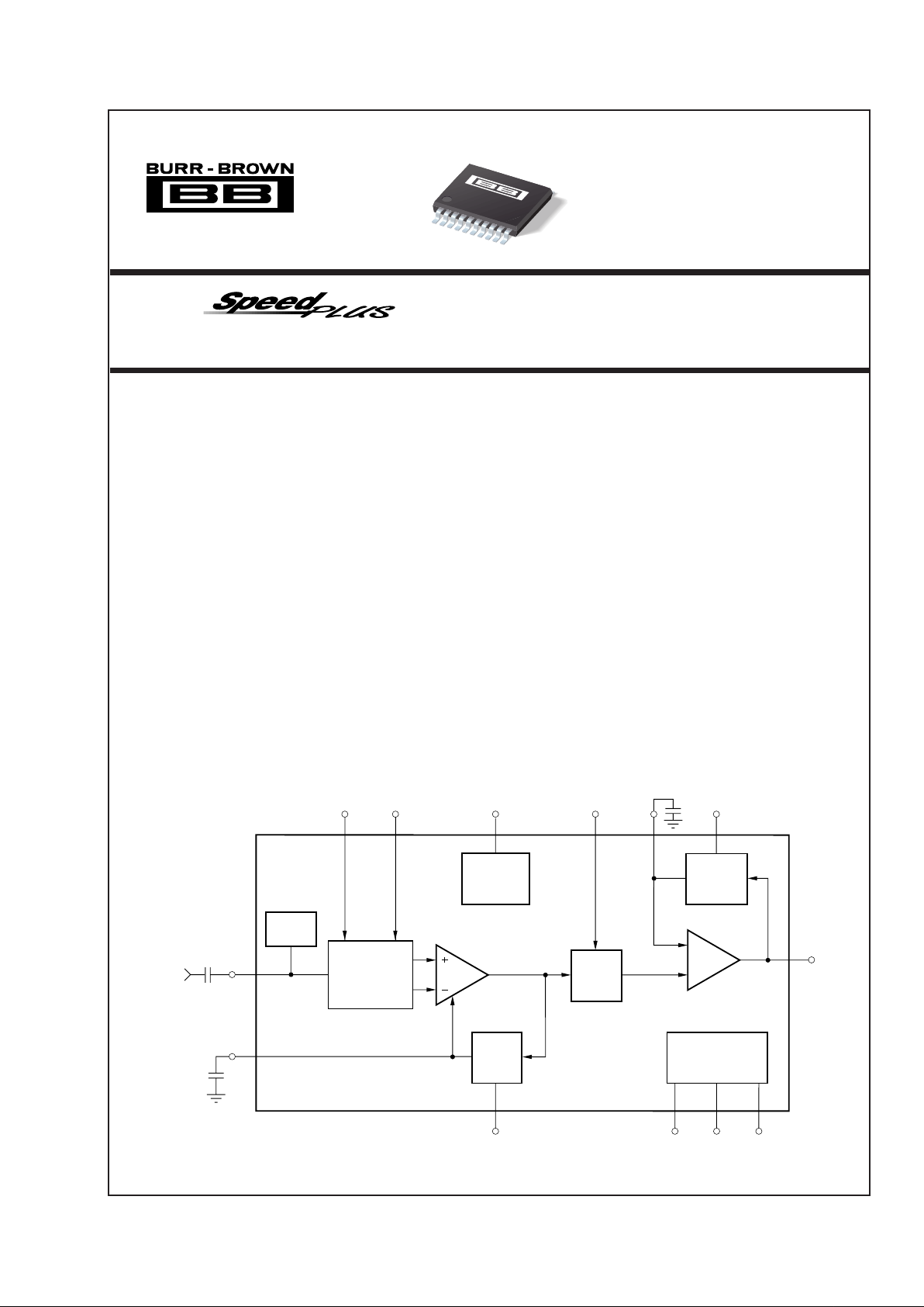
THEORY OF OPERATION
The VSP2080 contains all of the key features associated with
the processing of analog signals in a CCD video camera or
digital still camera. Figure 1 shows a simplified block
diagram of the VSP2080. The output from the CCD array is
first clamped to an internal reference of +1V. This sets the
proper signal range for the input of the Correlated Double
Sampler (CDS). The CDS operates at at gain of 2 and
provides a differential output. Its output drives a voltagecontrolled attenuator with a logarithmic control characteristic. An output amplifier drives this signal to external circuitry and sets the proper black level for the ADS900 A/D
converter.
CORRELATED DOUBLE SAMPLER (CDS)
The CDS removes low frequency noise from the output of
the image sensor. Refer to Figure 2 which shows a block
diagram of the CDS. The output from the CCD array is
sampled during the reference interval as well as during the
data interval. Noise that is present at the input and is of a
period greater than the pixel interval will be eliminated by
subtraction.
The VSP2080 employs a three track-and-hold correlated
double sampler architecture. Track/Hold 2 samples the CCD
noise during the reference interval as driven by the REFCK
signal. Track/Hold 3 resamples this level at the same time
that Track/Hold 1 samples the video information as driven
by the DATCK signal. This is done to remove large transients from Track/Hold 2 that result from a portion of the
reset transient being present during the acquisition time of
this track-and-hold. The output of Track/Hold 2 is buffered
by a voltage follower.
FIGURE 2. Simplified Block Diagram of Correlated Double Sampler.
FIGURE 1. Simplified Block Diagram of VSP2080.
VCACDS
Clamp
REFCK DATCK
Black Level
Auto-Zero
Loop
Dummy
Feedback
Loop
OB
Gain Control
DUMC
Output
Amplifier
Analog
Output
CCD D
CCD
OUT
C
EXT
Data Sampling Channel
Reference Sampling
Channel
T/H1
T/H3
T/H2
1V
DUMC REFCK
DATCK
To VCA
CCD D
CCD
OUT
C
EXT
Page 6

®
6
VSP2080
DIFFERENCE AMPLIFIER
The correlated double sampler function is completed when
the output of the data and reference channel are sent to the
difference amplifier where the signals are subtracted. In
addition to providing the difference function, the difference
amplifier amplifies the signal by a factor of 2 which helps
to improve the overall signal-to-noise ratio. The difference
amplifier also generates a differential signal to drive the
voltage-controlled attenuator.
INPUT CLAMP
The output from the CCD array is capacitively coupled to the
VSP2080. T o prevent shifts in the DC level from taking place
due to varying input duty cycles, the input capacitor is
clamped during the dummy pixel interval by the REFCK
signal. A P-channel transistor is used for this input clamp
switch to be able to allow a 2V negative change at the input
that would bring the signal below ground by 1V. Under
typical conditions, the black level at the input to the VSP2080
is at 1V.
DUMMY PIXEL AUTO-ZERO LOOP
The output from the data and reference channel is processed
by the previously mentioned difference amplifier. The differential output from the difference amplifier is sent to both
the voltage-controlled logarithmic attenuator and to an error
amplifier. The error amplifier amplifies and feeds a signal to
the difference amplifier to drive the offset measured at the
output of the difference amplifier to zero. A block diagram
of this circuit is shown in Figure 3. This error amplifier
serves the purpose of reducing the offset of the CDS to avoid
a large offset from being amplified by the output amplifier.
The effective time constant of this loop is given by:
where R is 10kΩ, C is an external capacitor connected to
CCD R (pin 14), A is the gain of the error amplifier with a
value of 50, and D is the duty cycle of the time that the dummy
pixel auto-zero loop is in operation. The duty cycle (D) must
be considered as the loop operates in a sampled mode. Operation of the dummy auto-zero loop is activated by the DUMC
signal that happens once during each horizontal line interval.
TIMING
The REFCK and DATCK signals are used to operate the
CDS as previously explained. The input digital timing signals REFCK, DATCK, DUMC and OB are capable of being
driven from either 3V or 5V logic levels.
VOLTAGE-CONTROLLED ATTENUATOR
To maximize the dynamic range of the VSP2080, a voltagecontrolled attenuator is included with a control range from
0dB to –34dB. The gain control has a logarithmic relationship between the control voltage and the attenuation. The
attenuator processes a differential signal from the difference
amplifier to improve linearity and to reject both power supply
and common-mode noise. The output from the attenuator is
amplified by 28dB prior to being applied to the A/D. A typical
gain control characteristic of the VSP2080 is shown in the
typical performance curve, “Gain Control Characteristics”.
BLACK LEVEL AUTO-ZERO LOOP
The black level auto-zero loop amplifies the difference
between the output of the output amplifier and a reference
signal during the dummy pixel interval. This difference
signal is amplified and fed back into the output amplifier to
correct the offset. In doing so, the output level of the entire
CCD channel can be controlled to be approximately –FS +
31mV under zero signal conditions. The black level autozero loop is activated by the OB timing signal. Figure 4
shows a block diagram of the black level auto-zero loop. The
loop time constant is given by:
where C is the external filter capacitance applied to C (pin 4),
GM is .001 Siemens (inverse ohm) and D is the duty cycle
of the time that the black level auto-zero loop is in operation.
The duty cycle (D) must be considered as the loop operates
in a sampled mode. Operation of the black level auto-zero
loop is activated by the OB signal that happens once during
each horizontal line interval.
FIGURE 3. Simplified Block Diagram of Dummy Pixel
Loop.
FIGURE 4. Simplified Block Diagram of Optical Black
Level Auto-Zero Loop.
T
C
GD
M
=
•
DUMC
To VCA
CDS
Error
Amplifier
A
CCD D
CCD R
R
C
EXT
OUT
1.03 • REF IN
Error
Amplifier
Output Amplifier
G
M
From
VCA
C
C
EXT
OB
T
RC
AD
=
•
•
Page 7

®
7
VSP2080
FIGURE 5. VSP2080 Typical Application and Bypassing Requirements.
DECOUPLING AND GROUNDING
CONSIDERATIONS
Figure 5 shows the recommended decoupling scheme for
the VSP2080. In most cases, 0.1µF ceramic chip capacitors
are adequate to keep the impedance low over a wide frequency range. Their effectiveness largely depends on the
proximity to the individual pin. Therefore, they should be
located as close as possible to the pins. In addition, one
larger capacitor (1µF to 22µF) should be connected from
V
DDA
to ground and placed on the PC board in proximity of
the VSP2080.
LCM
2.4V
OUT
C
MODE
OB
REFCK
DATCK
DUMC
PD
REF IN
REFB
REFT
V
DDA
AGC IN
GND
A
CCD R
CCD D
GND
A
V
DDA
1
2
3
4
5
6
7
8
9
10
20
19
18
17
16
15
14
13
12
11
VSP2080
0.1µF
0.1µF
0.1µF
0.1µF
0.1µF
0.1µF
0.1µF
0.1µF
0.1µF
0.1µF
DSP
ADS900
Analog
Input
Reference Out (1.0V)
0.047µF
CCD Output
V
DDA
A/D Converter
 Loading...