

Page 1
Vishay Semiconductors
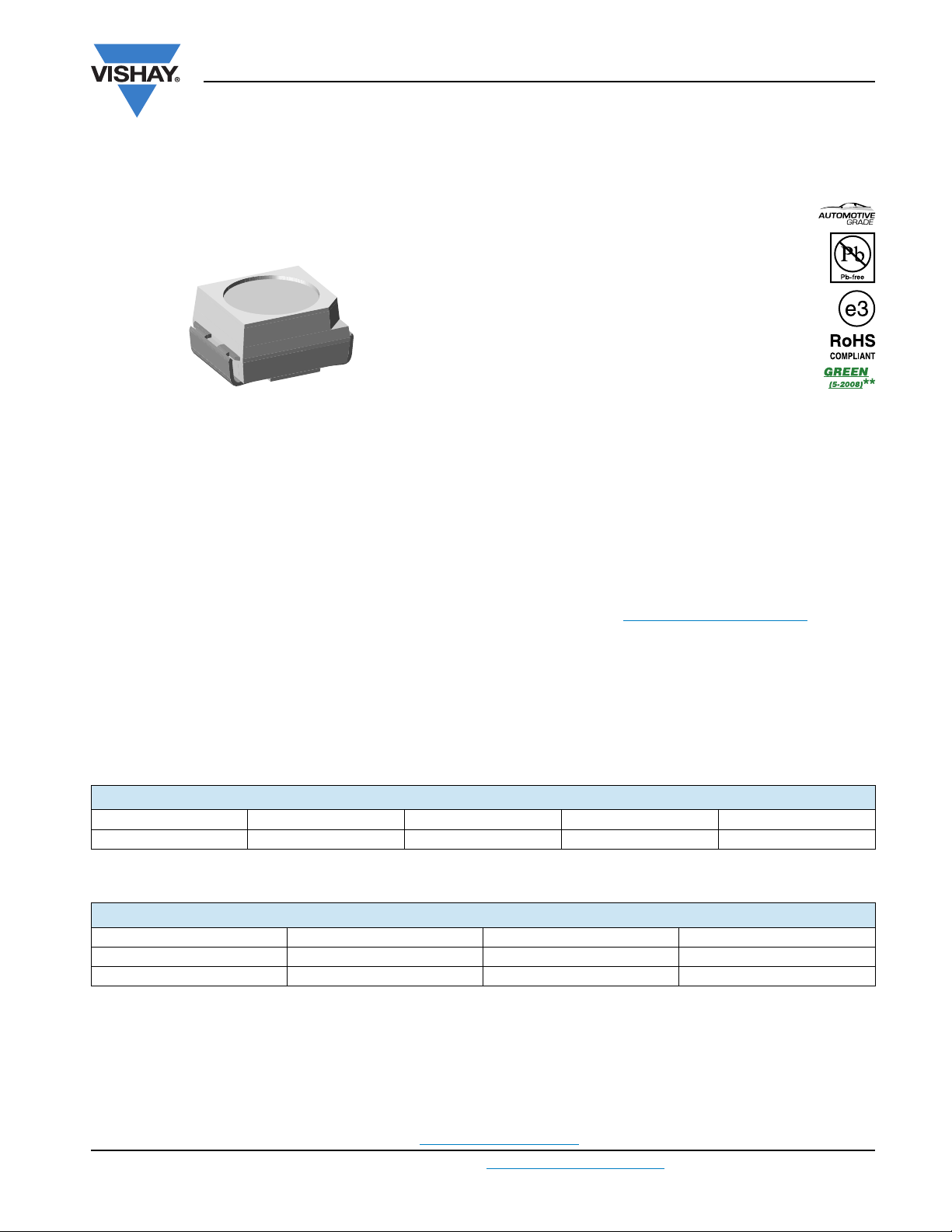
High Power Infrared Emitting Diode, 940 nm, GaAlAs/GaAs
FEATURES
• Package type: surface mount
• Package form: PLCC-2
• Dimensions (L x W x H in mm): 3.5 x 2.8 x 1.75
94 8553
DESCRIPTION
VSML3710 is an infrared, 940 nm emitting diode in
GaAlAs/GaAs technology with high radiant power, molded
in a PLCC-2 package for surface mounting (SMD).
• Peak wavelength: λ
• High reliability
• High radiant power
• High radiant intensity
• Angle of half intensity: ϕ = ± 60°
• Low forward voltage
• Suitable for high pulse current operation
• Good spectral matching with Si photodetectors
• Package matched with IR emitter series VEMT3700
• Floor life: 168 h, MSL 3, acc. J-STD-020
• Lead (Pb)-free reflow soldering
• AEC-Q101 qualified
• Compliant to RoHS directive 2002/95/EC and in
accordance to WEEE 2002/96/EC
• Find out more about Vishay’s Automotive Grade Product
requirements at: www.vishay.com/applications
= 940 nm
p
VSML3710
APPLICATIONS
• IR emitter in photointerrupters, sensors and reflective
sensors
• IR emitter in low space applications
• Household appliance
• Tactile keyboards
PRODUCT SUMMARY
COMPONENT Ie (mW/sr) ϕ (deg) λp (nm) tr (ns)
VSML3710 8 ± 60 940 800
Note
Test conditions see table “Basic Characteristics”
ORDERING INFORMATION
ORDERING CODE PACKAGING REMARKS PACKAGE FORM
VSML3710-GS08 Tape and reel MOQ: 7500 pcs, 1500 pcs/reel PLCC-2
VSML3710-GS18 Tape and reel MOQ: 8000 pcs, 8000 pcs/reel PLCC-2
Note
MOQ: minimum order quantity
** Please see document “Vishay Material Category Policy”: www.vishay.com/doc?99902
www.vishay.com
Page 2
VSML3710
Vishay Semiconductors
High Power Infrared Emitting Diode,
940 nm, GaAlAs/GaAs
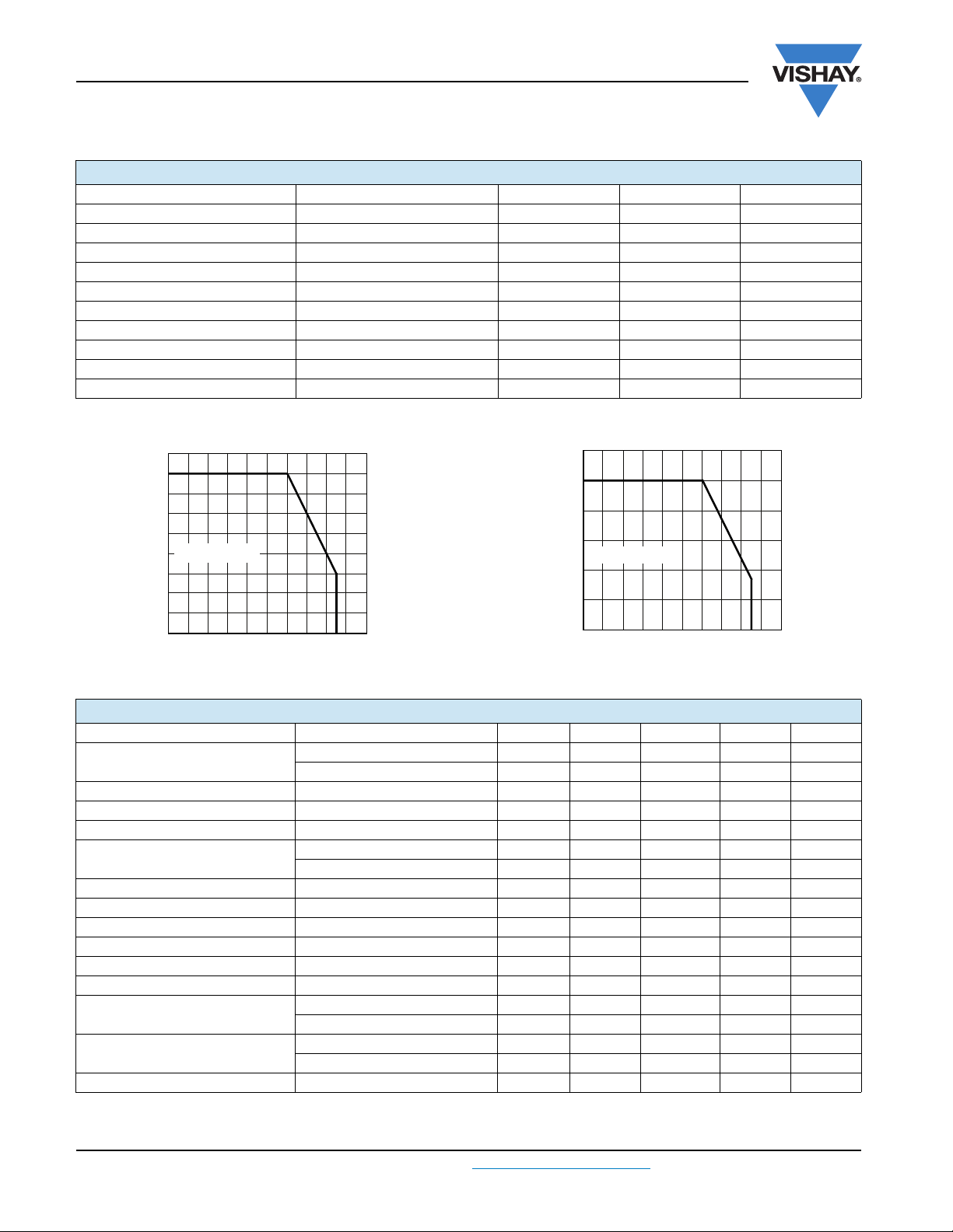
ABSOLUTE MAXIMUM RATINGS
PARAMETER TEST CONDITION SYMBOL VALUE UNIT
Reverse voltage V
Forward current I
Peak forward current t
Surge forward current t
/T = 0.5, tp = 100 μs I
p
= 100 μs I
p
Power dissipation P
Junction temperature T
Operating temperature range T
Storage temperature range T
Soldering temperature Acc. figure 11, J-STD-020 T
Thermal resistance junction/ambient J-STD-051, soldered on PCB R
Note
= 25 °C, unless otherwise specified
T
amb
180
160
140
120
100
R
80
60
40
- Power Dissipation (mW)
V
P
20
21343
= 250 K/W
thJA
0
0 102030405060708090100
T
- Ambient Temperature (°C)
amb
R
F
FM
FSM
V
j
amb
stg
sd
thJA
120
100
80
60
R
= 250 K/W
thJA
40
- Forward Current (mA)
F
I
20
0
0 10 203040 50607080 90100
21344
- Ambient Temperature (°C)
T
amb
Fig. 1 - Power Dissipation Limit vs. Ambient Temperature Fig. 2 - Forward Current Limit vs. Ambient Temperature
5V
100 mA
200 mA
1A
160 mW
100 °C
- 40 to + 85 °C
- 40 to + 100 °C
260 °C
250 K/W
BASIC CHARACTERISTICS
PARAMETER TEST CONDITION SYMBOL MIN. TYP. MAX. UNIT
I
= 100 mA, tp = 20 ms V
Forward voltage
Temperature coefficient of V
F
F
I
= 1 A, tp = 100 μs V
F
Reverse current V
Junction capacitance V
Radiant intensity
Radiant power I
Temperature coefficient of φ
e
= 0 V, f = 1 MHz, E = 0 C
R
= 100 mA, tp = 20 ms I
I
F
I
= 1 A, tp = 100 μs I
F
= 100 mA, tp = 20 ms φ
F
IF = 100 mA TKφ
IF = 1 mA TK
= 5 V I
R
F
F
VF
R
j
e
e
e
e
4820mW/sr
Angle of half intensity ϕ ± 60 deg
Peak wavelength I
Spectral bandwidth I
Temperature coefficient of λ
p
Rise time
Fall time
= 100 mA λ
F
= 100 mA Δλ 50 nm
F
IF = 100 mA TKλ
I
= 20 mA t
F
I
= 1 A t
F
I
= 20 mA t
F
I
= 1 A t
F
p
p
r
r
f
f
Virtual source diameter d 0.44 mm
Note
T
= 25 °C, unless otherwise specified
amb
1.35 1.6 V
2.6 3 V
- 1.8 mV/K
100 μA
25 pF
60 mW/sr
35 mW
- 0.6 %/K
940 nm
0.2 nm/K
800 ns
500 ns
800 ns
500 ns
Document Number: 81300
Page 3
VSML3710
BASIC CHARACTERISTICS
T
= 25 °C, unless otherwise specified
amb
10 000
tp/T = 0.005
1000
100
0.2
0.5
DC
10
- Forward Current (mA)
F
I
1
0.01 0.1 1 10
95 9985
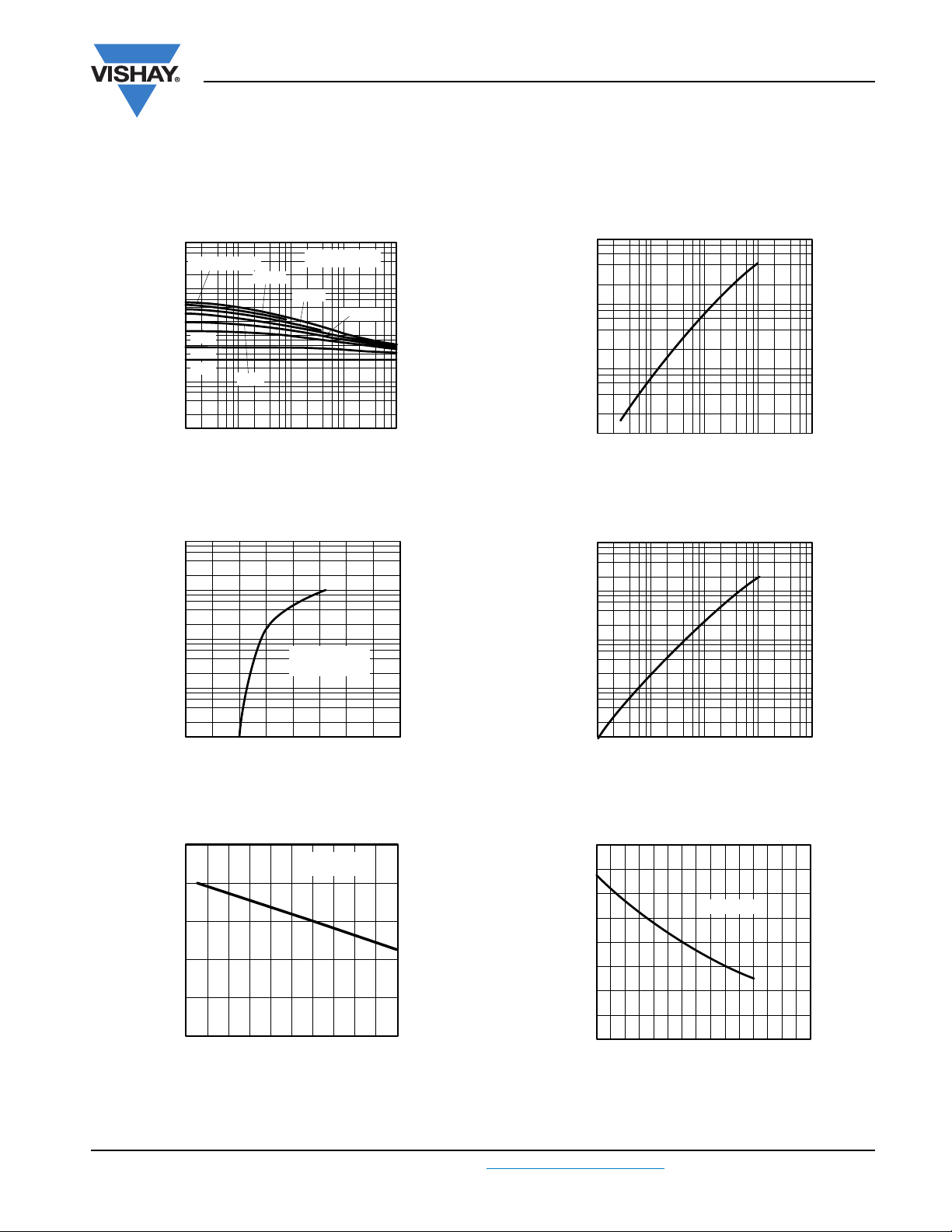
Fig. 3 - Pulse Forward Current vs. Pulse Duration
4
10
0.01
0.1
tp - Pulse Length (ms)
High Power Infrared Emitting Diode,
940 nm, GaAlAs/GaAs
T
< 60 °C
amb
0.02
0.05
100
15903
Vishay Semiconductors
100
10
1
e
I - Radiant Intensity (mW/sr)
0.1
10
0
10
1
10
2
I F- Forward Current (mA)
Fig. 6 - Radiant Intensity vs. Forward Current
1000
10
3
10
4
3
10
2
10
tP = 100 µs
t
/T = 0.001
1
10
- Forward Current (mA)
F
I
0
10
13600
0
1
VF - Forward Voltage (V)
P
32
Fig. 4 - Forward Current vs. Forward Voltage
1.2
IF = 1 mA
1.1
1.0
0.9
- Forward Voltage (V)
F
I
0.8
0.7
0 102030405060708090100
16848
- Ambient Temperature (°C)
T
amb
100
10
- Radiant Power (mW)
1
e
Φ
0.1
4
94 8740
10
0
10
1
10
2
I F- Forward Current (mA)
10
3
10
4
Fig. 7 - Radiant Power vs. Forward Current
1.6
1.2
e rel
Φ
;
0.8
e rel
I
0.4
0
- 10 10 50 0 100
T
94 7993
- Ambient Temperature (°C)
amb
IF = 20 mA
140
Fig. 5 - Forward Voltage vs. Ambient Temperature
Fig. 8 - Relative Radiant Intensity/Power vs. Ambient Temperature
Document Number: 81300 For technical questions, contact: [email protected]
www.vishay.com
Rev. 1.4, 03-Nov-09 3
Page 4
VSML3710
Vishay Semiconductors
1.25
1.0
0.75
0.5
- Relative Radiant Power
0.25
e rel
Φ
14291
0
890
IF = 100 mA
- Wavelength (nm)
λ
High Power Infrared Emitting Diode,
940
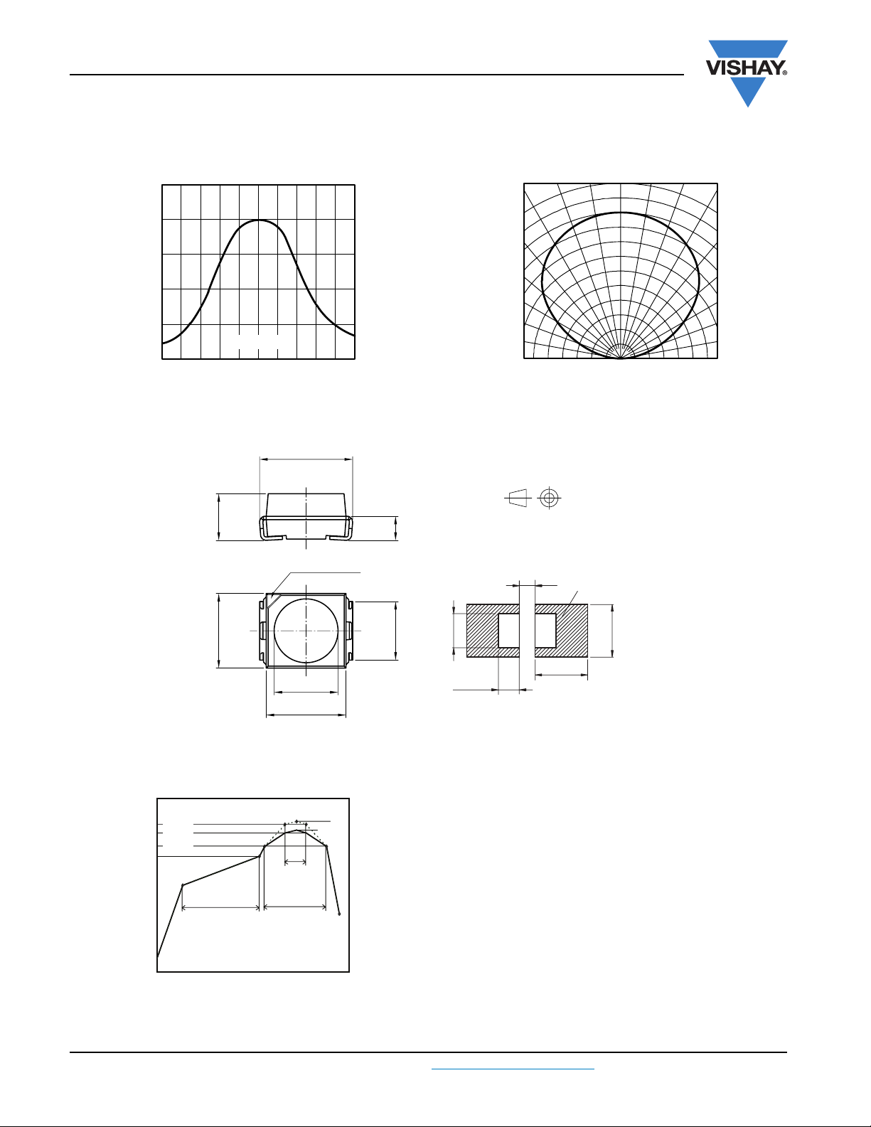
Fig. 9 - Relative Radiant Power vs. Wavelength Fig. 10 - Relative Radiant Intensity vs. Angular Displacement
PACKAGE DIMENSIONS in millimeters
± 0.2
3.5
940 nm, GaAlAs/GaAs
- Relative Radiant Intensity
e, rel
I
990
94 8013
1.0
0.9
0.8
0.7
0.6
0.4 0.2 0
0°
10° 20°
30°
40°
50°
60°
70°
ϕ - Angular Displacement
80°
± 0.1
1.75
Pin identification
± 0.15
CA
2.8
Ø 2.4
+ 0.15
3
Drawing-No.: 6.541-5067.01-4
Issue: 5; 04.11.08
20541
SOLDER PROFILE
300
255 °C
250
240 °C
217 °C
200
150
100
max. 120 s
Temperature (°C)
50
max. ramp up 3 °C/s
0
0 50 100 150 200 250 300
19841
max. ramp down 6 °C/s
Time (s)
Fig. 11 - Lead (Pb)-free Reflow Solder Profile acc. J-STD-020
max. 260 °C
245 °C
max. 30 s
max. 100 s
0.9
2.2
2.6 (2.8)
1.6 (1.9)
DRYPACK
Devices are packed in moisture barrier bags (MBB) to
prevent the products from moisture absorption during
transportation and storage. Each bag contains a desiccant.
FLOOR LIFE
Floor life (time between soldering and removing from MBB)
must not exceed the time indicated on MBB label:
Floor life: 168 h
Conditions: T
Moisture sensitivity level 3, acc. to J-STD-020.
DRYING
In case of moisture absorption devices should be baked
before soldering. Conditions see J-STD-020 or label.
Devices taped on reel dry using recommended conditions
192 h at 40 °C (+ 5 °C), RH < 5 %.
technical drawings
according to DIN
specifications
Mounting Pad Layout
1.2
4
< 30 °C, RH < 60 %
amb
area covered with
solder resist
4
www.vishay.com For technical questions, contact: [email protected]
Document Number: 81300
4 Rev. 1.4, 03-Nov-09
Page 5
VSML3710
High Power Infrared Emitting Diode,
940 nm, GaAlAs/GaAs
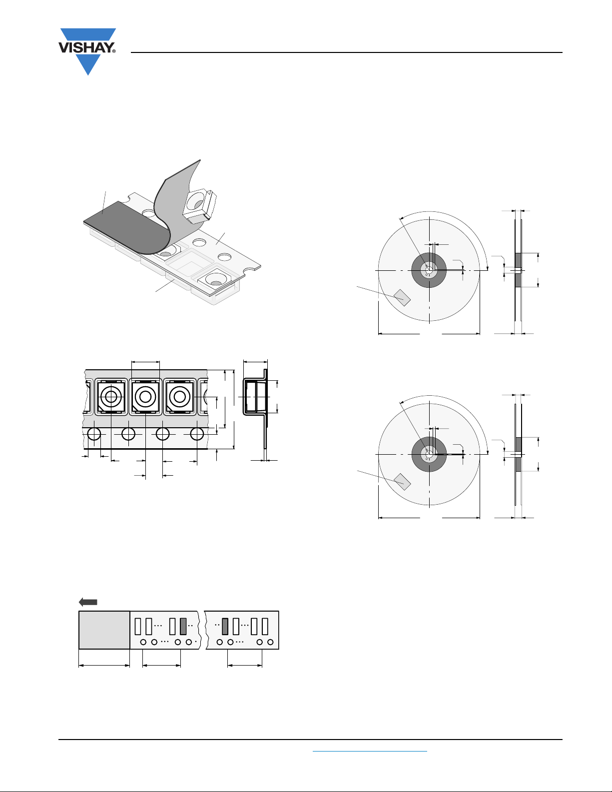
TAPE AND REEL
PLCC-2 components are packed in antistatic blister tape
(DIN IEC (CO) 564) for automatic component insertion.
Cavities of blister tape are covered with adhesive tape.
Adhesive tape
Blister tape
Component cavity
Fig. 12 - Blister Tape
3.5
3.1
2.2
2.0
94 8670
Vishay Semiconductors
The tape leader is at least 160 mm and is followed by a
carrier tape leader with at least 40 empty compartments.
The tape leader may include the carrier tape as long as the
cover tape is not connected to the carrier tape. The least
component is followed by a carrier tape trailer with a least
75 empty compartments and sealed with cover tape.
10.0
13.00
12.75
14.4 max.
9.0
63.5
60.5
94 8665
Identification
Label:
Vishay
type
group
tape code
production
code
quantity
120°
4.5
3.5
2.5
1.5
180
178
Fig. 15 - Dimensions of Reel-GS08
5.75
1.6
1.4
4.1
3.9
2.05
1.95
4.1
3.9
3.6
3.4
1.85
1.65
5.25
8.3
7.7
0.25
94 8668
4.0
3.6
Fig. 13 - Tape Dimensions in mm for PLCC-2
MISSING DEVICES
A maximum of 0.5 % of the total number of components per
reel may be missing, exclusively missing components at the
beginning and at the end of the reel. A maximum of three
consecutive components may be missing, provided this gap
is followed by six consecutive components.
> 160 mm
Tape leader
De-reeling direction
40 empty
compartments
Carrier leader Carrier trailer
min. 75 empty
compartments
Fig. 14 - Beginning and End of Reel
94 8158
10.4
13.00
12.75
14.4 max.
8.4
62.5
60.0
18857
Identification
Label:
Vishay
type
group
tape code
production
code
quantity
321
329
4.5
3.5
120°
2.5
1.5
Fig. 16 - Dimensions of Reel-GS18
COVER TAPE REMOVAL FORCE
The removal force lies between 0.1 N and 1.0 N at a removal
speed of 5 mm/s. In order to prevent components from
popping out of the blisters, the cover tape must be pulled off
at an angle of 180° with regard to the feed direction.
Document Number: 81300 For technical questions, contact: [email protected]
www.vishay.com
Rev. 1.4, 03-Nov-09 5
Page 6

Legal Disclaimer Notice
Vishay
Disclaimer
All product specifications and data are subject to change without notice.
Vishay Intertechnology, Inc., its affiliates, agents, and employees, and all persons acting on its or their behalf
(collectively, “Vishay”), disclaim any and all liability for any errors, inaccuracies or incompleteness contained herein
or in any other disclosure relating to any product.
Vishay disclaims any and all liability arising out of the use or application of any product described herein or of any
information provided herein to the maximum extent permitted by law. The product specifications do not expand or
otherwise modify Vishay’s terms and conditions of purchase, including but not limited to the warranty expressed
therein, which apply to these products.
No license, express or implied, by estoppel or otherwise, to any intellectual property rights is granted by this
document or by any conduct of Vishay.
The products shown herein are not designed for use in medical, life-saving, or life-sustaining applications unless
otherwise expressly indicated. Customers using or selling Vishay products not expressly indicated for use in such
applications do so entirely at their own risk and agree to fully indemnify Vishay for any damages arising or resulting
from such use or sale. Please contact authorized Vishay personnel to obtain written terms and conditions regarding
products designed for such applications.
Product names and markings noted herein may be trademarks of their respective owners.
Document Number: 91000 www.vishay.com
Revision: 18-Jul-08 1
 Loading...