

Page 1
www.vishay.com
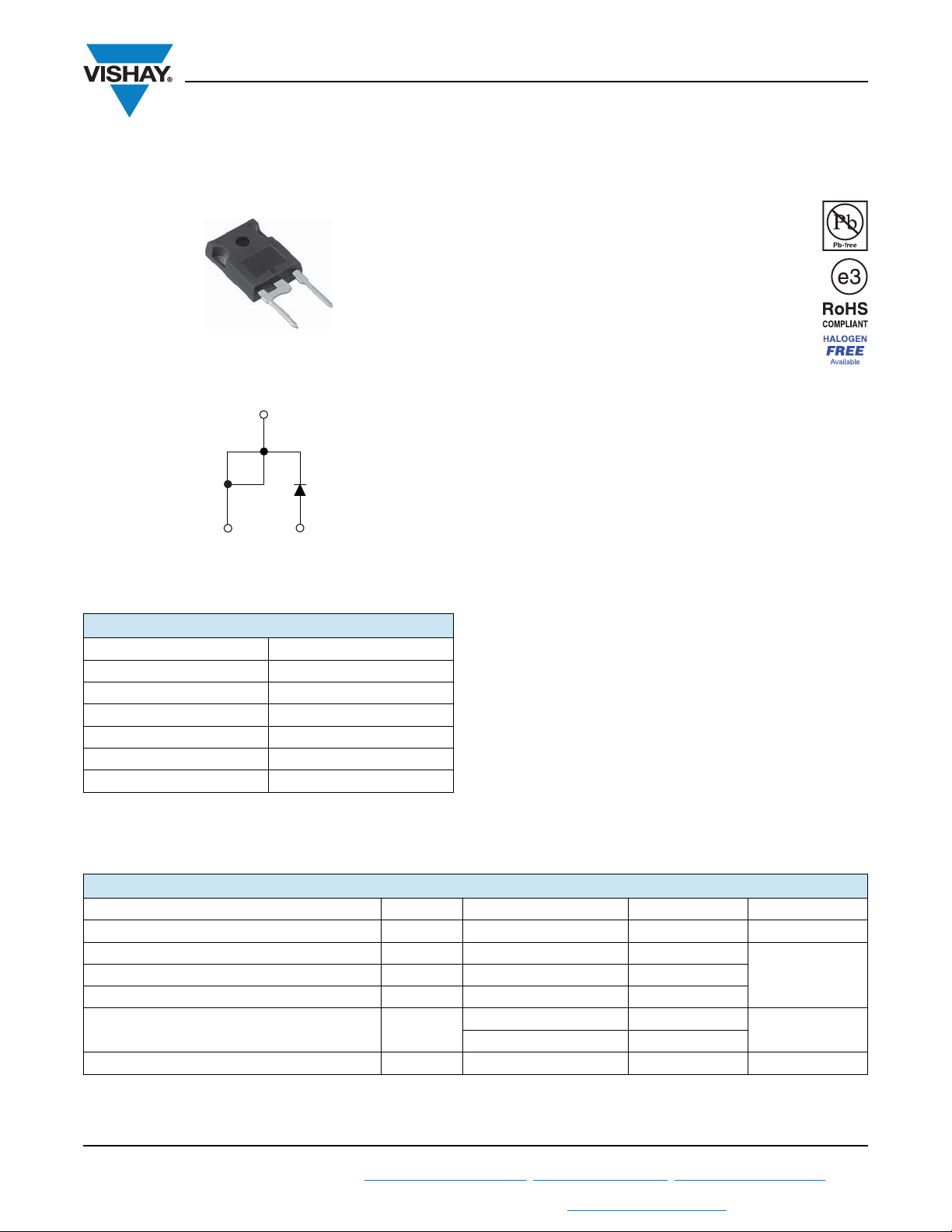
TO-247AC modified
Ultrafast Soft Recovery Diode, 15 A
VS-HFA15PB60PbF, VS-HFA15PB60-N3
Vishay Semiconductors
HEXFRED®
FEATURES
• Ultrafast and ultrasoft recovery
• Very low I
• Compliant to RoHS Directive 2002/95/EC
• Designed and qualified according to
JEDEC-JESD47
• Halogen-free according to IEC 61249-2-21
definition (-N3 only)
RRM
and Q
rr
Base
common
cathode
2
13
Cathode
Anode
PRODUCT SUMMARY
Package TO-247AC modified (2 pins)
I
F(AV)
V
R
V
at I
F
F
t
typ. 19 ns
rr
max. 150 °C
T
J
Diode variation Single die
15 A
600 V
1.7 V
BENEFITS
• Reduced RFI and EMI
• Reduced power loss in diode and switching transistor
• Higher frequency operation
• Reduced snubbing
• Reduced parts count
DESCRIPTION
VS-HFA15PB60... is a state of the art ultrafast recovery
diode. Employing the latest in epitaxial construction and
advanced processing techniques it features a superb
combination of characteristics which result in performance
which is unsurpassed by any rectifier previously available.
With basic ratings of 600 V and 15 A continuous current, the
VS-HFA15PB60... is especially well suited for use as the
companion diode for IGBTs and MOSFETs. In addition to
ultrafast recovery time, the HEXFRED
extremely low values of peak recovery current (I
does not exhibit any tendency to “snap-off” during the t
portion of recovery. The HEXFRED features combine to offer
designers a rectifier with lower noise and significantly lower
switching losses in both the diode and the switching
transistor. These HEXFRED advantages can help to
significantly reduce snubbing, component count and
heatsink sizes. The HEXFRED VS-HFA15PB60... is ideally
suited for applications in power supplies and power
conversion systems (such as inverters), motor drives, and
many other similar applications where high speed, high
efficiency is needed.
®
product line features
) and
RRM
b
ABSOLUTE MAXIMUM RATINGS
PARAMETER SYMBOL TEST CONDITIONS VALUES UNITS
Cathode to anode voltage V
Maximum continuous forward current I
Maximum repetitive forward current I
Maximum power dissipation P
Operating junction and storage temperature range T
Revision: 19-Aug-11
R
F
FSM
FRM
D
, T
J
For technical questions within your region: [email protected]
THIS DOCUMENT IS SUBJECT TO CHANGE WITHOUT NOTICE. THE PRODUCTS DESCRIBED HEREIN AND THIS DOCUMENT
ARE SUBJECT TO SPECIFIC DISCLAIMERS, SET FORTH AT www.vishay.com/doc?91000
TC = 100 °C 15
TC = 25 °C 74
T
= 100 °C 29
C
Stg
1
600 V
150
60
W
- 55 to + 150 °C
Document Number: 94052
ASingle pulse forward current I
Page 2
VS-HFA15PB60PbF, VS-HFA15PB60-N3
www.vishay.com
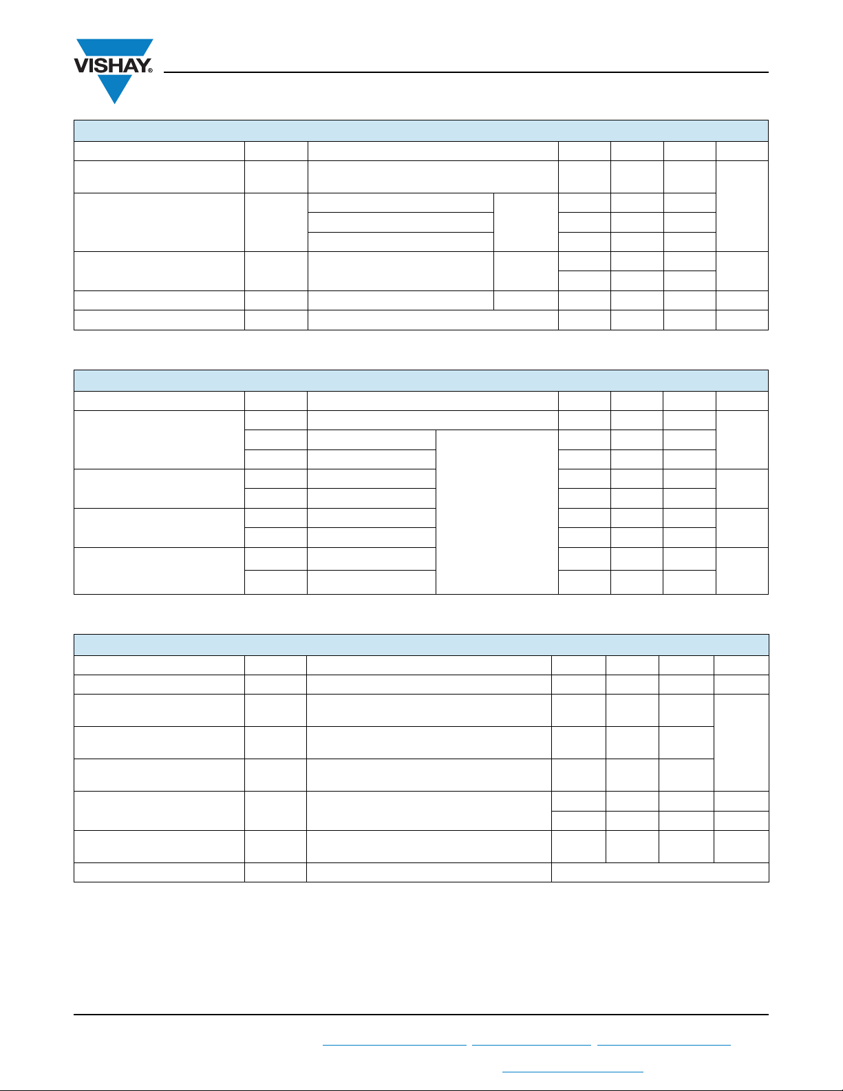
ELECTRICAL SPECIFICATIONS (TJ = 25 °C unless otherwise specified)
PARAMETER SYMBOL TEST CONDITIONS MIN. TYP. MAX. UNITS
Cathode to anode
breakdown voltage
V
BR
IR = 100 μA 600 - -
IF = 15 A
Maximum forward voltage V
Maximum reverse
leakage current
Junction capacitance C
Series inductance L
FM
I
RM
T
S
= 30 A - 1.5 2.0
I
F
I
= 15 A, TJ = 125 °C - 1.2 1.6
F
VR = VR rated
= 125 °C, VR = 0.8 x VR rated
T
J
See fig. 1
See fig. 2
VR = 200 V See fig. 3 - 25 50 pF
Measured lead to lead 5 mm from package body - 12 - nH
DYNAMIC RECOVERY CHARACTERISTICS (TJ = 25 °C unless otherwise specified)
PARAMETER SYMBOL TEST CONDITIONS MIN. TYP. MAX. UNITS
Reverse recovery time
See fig. 5, 10
Peak recovery current
See fig. 6
Reverse recovery charge
See fig. 7
Peak rate of fall of
recovery current during t
See fig. 8
t
rr
rr1
t
rr2
I
RRM1
I
RRM2
Q
rr1
Q
rr2
dI
b
dI
(rec)M
(rec)M
IF = 1.0 A, dIF/dt = 200 A/μs, VR = 30 V - 19 -
TJ = 25 °C
TJ = 125 °C - 74 120
TJ = 25 °C - 4.0 6.0
= 15 A
TJ = 125 °C - 6.5 10
TJ = 25 °C - 80 180
TJ = 125 °C - 220 600
I
F
/dt = 200 A/μs
dI
F
V
= 200 V
R
/dt1 TJ = 25 °C - 188 -
/dt2 TJ = 125 °C - 160 -
Vishay Semiconductors
-1.31.7
-1.010
- 400 1000
-4260
V
μA
nst
A
nC
A/μs
THERMAL - MECHANICAL SPECIFICATIONS
PARAMETER SYMBOL TEST CONDITIONS MIN. TYP. MAX. UNITS
Lead temperature T
Thermal resistance,
junction to case
Thermal resistance,
junction to ambient
Thermal resistance,
case to heatsink
R
R
R
lead
thJC
thJA
thCS
Weight
Mounting torque
Marking device Case style TO-247AC modified (JEDEC) HFA15PB60
Revision: 19-Aug-11
For technical questions within your region: [email protected]
THIS DOCUMENT IS SUBJECT TO CHANGE WITHOUT NOTICE. THE PRODUCTS DESCRIBED HEREIN AND THIS DOCUMENT
ARE SUBJECT TO SPECIFIC DISCLAIMERS, SET FORTH AT www.vishay.com/doc?91000
0.063" from case (1.6 mm) for 10 s - - 300 °C
--1.7
Typical socket mount - - 40
Mounting surface, flat, smooth and greased - 0.25 -
-6.0- g
-0.21- oz.
6.0
(5.0)
2
-
Document Number: 94052
12
kgf · cm
(10)
(lbf · in)
K/W
Page 3
www.vishay.com
1
10
1.0 2.41.2 1.4
VFM - Forward Voltage Drop (V)
I
F
- Instantaneous Forward Current (A)
100
1.8 2.22.01.6
TJ = 150 °C
T
J
= 125 °C
T
J
= 25 °C
10
100
10 100 1000
VR - Reverse Voltage (V)
C
T
- Junction Capacitance (pF)
TJ = 25 °C
VS-HFA15PB60PbF, VS-HFA15PB60-N3
Vishay Semiconductors
10 000
1000
TJ = 150 °C
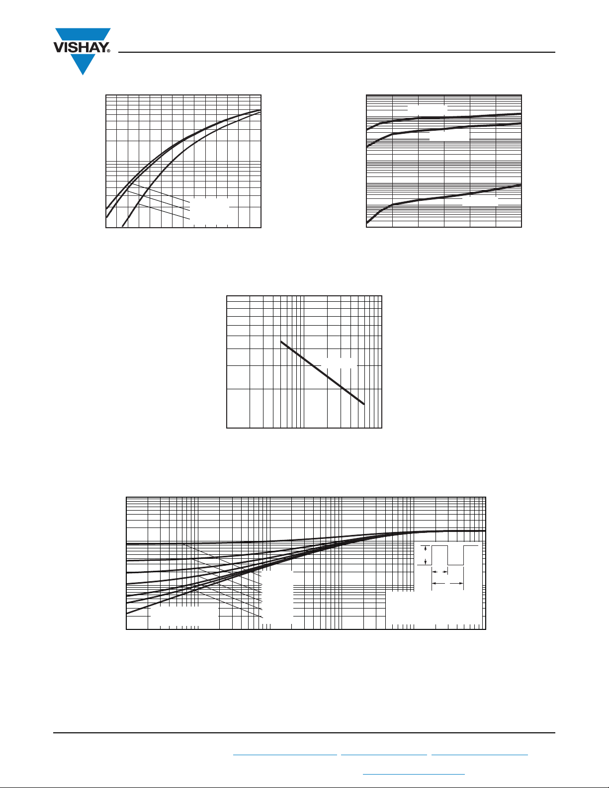
Fig. 1 - Maximum Forward Voltage Drop vs.
Instantaneous Forward Current
100
10
- Reverse Current (μA)
R
0.1
I
0.01
1
0
100 600500
TJ = 125 °C
300
TJ = 25 °C
400200
VR - Reverse Voltage (V)
Fig. 2 - Typical Reverse Current vs. Reverse Voltage
- Thermal Response
thJC
Z
Revision: 19-Aug-11
For technical questions within your region: [email protected]
THIS DOCUMENT IS SUBJECT TO CHANGE WITHOUT NOTICE. THE PRODUCTS DESCRIBED HEREIN AND THIS DOCUMENT
Fig. 3 - Typical Junction Capacitance vs. Reverse Voltage
10
1
D = 0.50
0.1
Single pulse
(thermal response)
0.01
0.00001 0.0001 0.001 0.01 0.1
D = 0.20
D = 0.10
D = 0.05
D = 0.02
D = 0.01
Notes:
1. Duty factor D = t
2. Peak TJ = PDM x Z
t1 - Rectangular Pulse Duration (s)
Fig. 4 - Maximum Thermal Impedance Z
ARE SUBJECT TO SPECIFIC DISCLAIMERS, SET FORTH AT www.vishay.com/doc?91000
3
Characteristics
thJC
P
DM
t
1
t
2
1/t2
+ T
thJC
C
1
Document Number: 94052
Page 4
www.vishay.com
80
40
0
100
1000
dIF/dt (A/µs)
t
rr
(ns)
VR = 200 V
T
J
= 125 °C
T
J
= 25 °C
60
20
100
IF = 30 A
I
F
= 15 A
I
F
= 5 A
20
15
0
100
1000
dIF/dt (A/µs)
I
rr
(A)
VR = 200 V
T
J
= 125 °C
T
J
= 25 °C
5
10
25
IF = 30 A
I
F
= 15 A
I
F
= 5 A
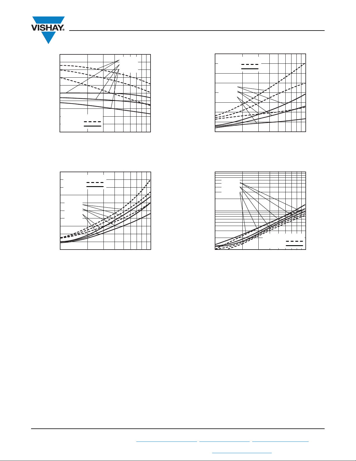
Fig. 5 - Typical Reverse Recovery Time vs. dIF/dt
VS-HFA15PB60PbF, VS-HFA15PB60-N3
Vishay Semiconductors
800
VR = 200 V
= 125 °C
T
J
= 25 °C
T
J
600
IF = 30 A
= 15 A
(nC)
rr
Q
10 000
I
400
F
= 5 A
I
F
200
0
100
dIF/dt (A/µs)
Fig. 7 - Typical Stored Charge vs. dI
IF = 30 A
= 15 A
I
F
= 5 A
I
F
1000
/dt
F
Fig. 6 - Typical Recovery Current vs. dI
1000
/dt (A/µs)
(rec)M
dI
VR = 200 V
= 125 °C
T
J
= 25 °C
T
100
100
J
1000
dIF/dt (A/µs)
/dt
F
Fig. 8 - Typical dI
/dt vs. dIF/dt
(rec)M
Revision: 19-Aug-11
4
For technical questions within your region: [email protected]
THIS DOCUMENT IS SUBJECT TO CHANGE WITHOUT NOTICE. THE PRODUCTS DESCRIBED HEREIN AND THIS DOCUMENT
ARE SUBJECT TO SPECIFIC DISCLAIMERS, SET FORTH AT www.vishay.com/doc?91000
Document Number: 94052
Page 5
www.vishay.com
Q
rr
0.5 I
RRM
dI
(rec)M
/dt
0.75 I
RRM
I
RRM
t
rr
t
b
t
a
I
F
dIF/dt
0
(1)
(2)
(3)
(4)
(5)
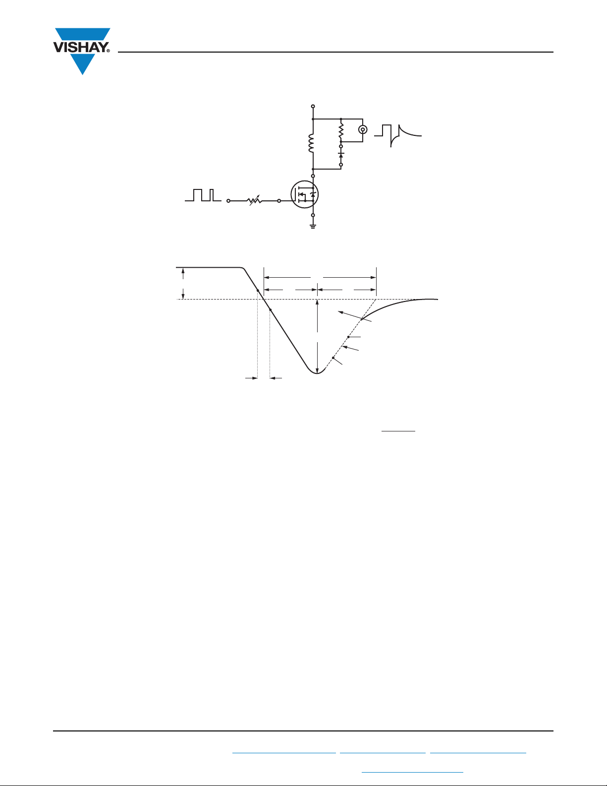
(1) dI
F
/dt - rate of change of current
through zero crossing
(2) I
RRM
- peak reverse recovery current
(3) t
rr
- reverse recovery time measured
from zero crossing point of negative
going I
F
to point where a line passing
through 0.75 I
RRM
and 0.50 I
RRM
extrapolated to zero current.
(4) Q
rr
- area under curve dened by t
rr
and I
RRM
trr x I
RRM
2
Q
rr
=
(5) dI
(rec)M
/dt - peak rate of change of
current during t
b
portion of t
rr
VS-HFA15PB60PbF, VS-HFA15PB60-N3
Vishay Semiconductors
= 200 V
V
R
0.01 Ω
L = 70 μH
D.U.T.
dIF/dt
adjust
G
D
IRFP250
S
Fig. 9 - Reverse Recovery Parameter Test Circuit
Revision: 19-Aug-11
For technical questions within your region: [email protected]
THIS DOCUMENT IS SUBJECT TO CHANGE WITHOUT NOTICE. THE PRODUCTS DESCRIBED HEREIN AND THIS DOCUMENT
Fig. 10 - Reverse Recovery Waveform and Definitions
ARE SUBJECT TO SPECIFIC DISCLAIMERS, SET FORTH AT www.vishay.com/doc?91000
5
Document Number: 94052
Page 6
www.vishay.com
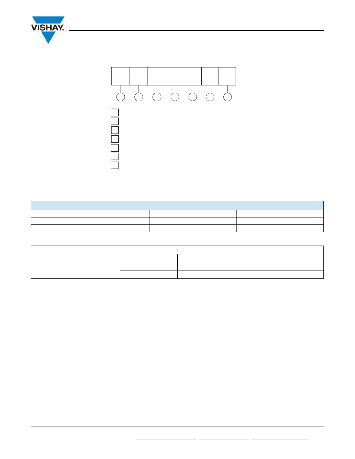
1 - Vishay Semiconductors product
2
- HEXFRED® family
3
- Electron irradiated
4
- Current rating (15 = 15 A)
5
- PB = TO-247AC modified
Device code
51 32 4 6 7
HFVS- A 15 PB 60 PbF
6
7
- Voltage rating: (60 = 600 V)
- Environmental digit:
PbF = Lead (Pb)-free and RoHS compliant
-N3 = Halogen-free, RoHS compliant and totally lead (Pb)-free
ORDERING INFORMATION TABLE
VS-HFA15PB60PbF, VS-HFA15PB60-N3
Vishay Semiconductors
ORDERING INFORMATION (Example)
PREFERRED P/N QUANTITY PER T/R MINIMUM ORDER QUANTITY PACKAGING DESCRIPTION
VS-HFA15PB60PbF 25 500 Antistatic plastic tube
VS-HFA15PB60-N3 25 500 Antistatic plastic tube
LINKS TO RELATED DOCUMENTS
Dimensions www.vishay.com/doc?95253
Part marking information
TO-247AC modified PbF www.vishay.com/doc?95225
TO-247AC modified -N3 www.vishay.com/doc?95442
Revision: 19-Aug-11
For technical questions within your region: [email protected]
THIS DOCUMENT IS SUBJECT TO CHANGE WITHOUT NOTICE. THE PRODUCTS DESCRIBED HEREIN AND THIS DOCUMENT
ARE SUBJECT TO SPECIFIC DISCLAIMERS, SET FORTH AT www.vishay.com/doc?91000
6
Document Number: 94052
Page 7
www.vishay.com
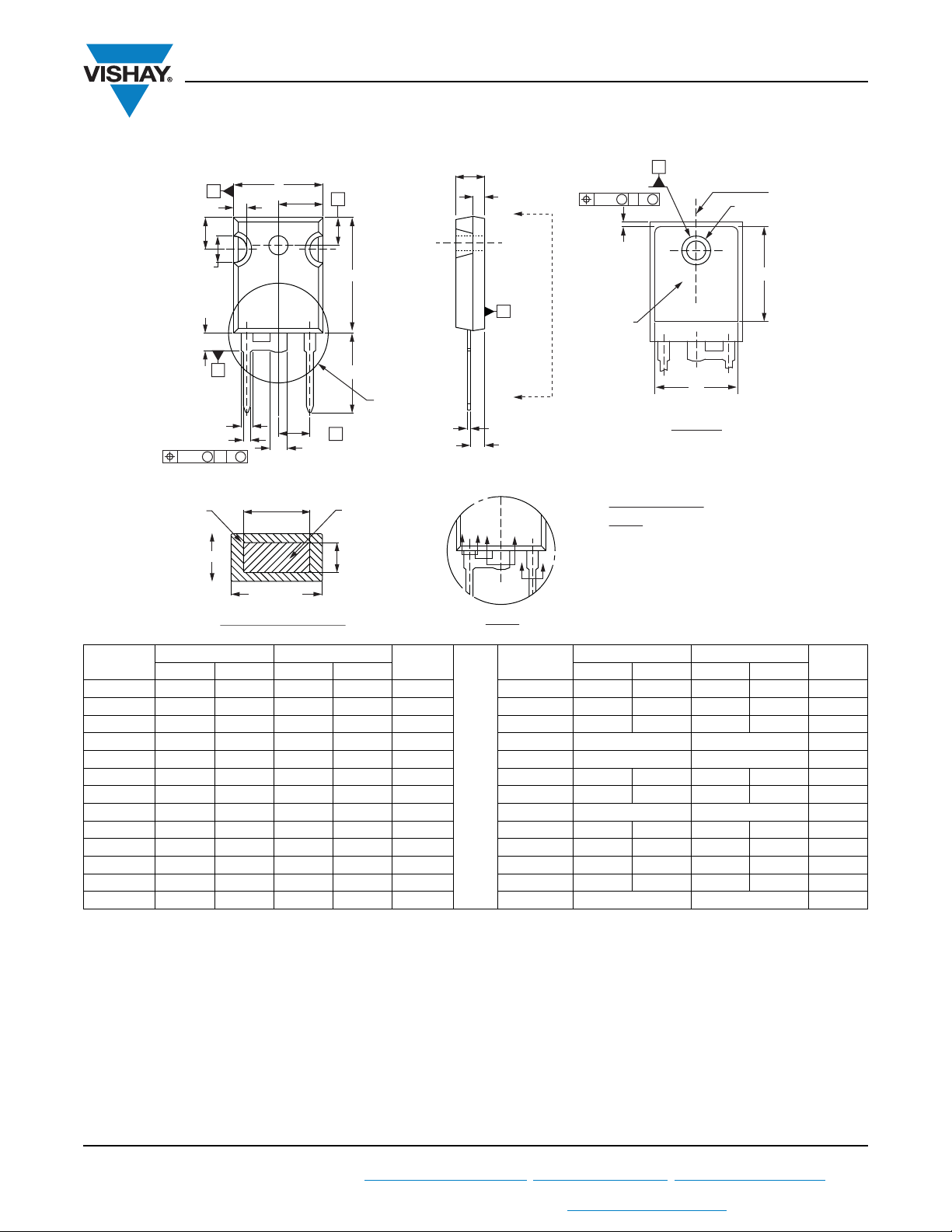
DIMENSIONS in millimeters and inches
Outline Dimensions
Vishay Semiconductors
(2) R/2
Q
2 x R
(2)
(5) L1
2 x b2
0.10 AC
Planting
(3)
B
C
3 x b
M M
(c)
Section C - C, D - D, E - E
E
1
2
b4
(b1, b3, b5)
(b, b2, b4)
N
3
(4)
2 x e
S
D
L
Base metal
c1
See view B
A
A2
A
D
A
C
A1
DDE E
View B
A
(6)
ΦP
M M
Ø K BD
D2
Thermal pad
Lead assignments
Diodes
1. - Anode/open
C
C
2. - Cathode
3. - Anode
(Datum B)
ΦP1
D1 (4)
4
(4)
E1
View A - A
SYMBOL
MILLIMETERS INCHES
MIN. MAX. MIN. MAX. MIN. MAX. MIN. MAX.
NOTES SYMBOL
MILLIMETERS INCHES
NOTES
A 4.65 5.31 0.183 0.209 D2 0.51 1.30 0.020 0.051
A1 2.21 2.59 0.087 0.102 E 15.29 15.87 0.602 0.625 3
A2 1.50 2.49 0.059 0.098 E1 13.72 - 0.540 -
b 0.99 1.40 0.039 0.055 e 5.46 BSC 0.215 BSC
b1 0.99 1.35 0.039 0.053 K 2.54 0.010
b2 1.65 2.39 0.065 0.094 L 14.20 16.10 0.559 0.634
b3 1.65 2.37 0.065 0.094 L1 3.71 4.29 0.146 0.169
b4 2.59 3.43 0.102 0.135 N 7.62 BSC 0.3
b5 2.59 3.38 0.102 0.133 P 3.56 3.66 0.14 0.144
c 0.38 0.86 0.015 0.034 P1 - 6.98 - 0.275
c1 0.38 0.76 0.015 0.030 Q 5.31 5.69 0.209 0.224
D 19.71 20.70 0.776 0.815 3 R 4.52 5.49 1.78 0.216
D1 13.08 - 0.515 - 4 S 5.51 BSC 0.217 BSC
Notes
(1)
Dimensioning and tolerance per ASME Y14.5M-1994
(2)
Contour of slot optional
(3)
Dimension D and E do not include mold flash. Mold flash shall not exceed 0.127 mm (0.005") per side. These dimensions are measured at
the outermost extremes of the plastic body
(4)
Thermal pad contour optional with dimensions D1 and E1
(5)
Lead finish uncontrolled in L1
(6)
P to have a maximum draft angle of 1.5 to the top of the part with a maximum hole diameter of 3.91 mm (0.154")
(7)
Outline conforms to JEDEC outline TO-247 with exception of dimension c
Revision: 21-Jun-11
For technical questions within your region: [email protected]
1
Document Number: 95253
THIS DOCUMENT IS SUBJECT TO CHANGE WITHOUT NOTICE. THE PRODUCTS DESCRIBED HEREIN AND THIS DOCUMENT
ARE SUBJECT TO SPECIFIC DISCLAIMERS, SET FORTH AT www.vishay.com/doc?91000
Page 8

Legal Disclaimer Notice
www.vishay.com
Vishay
Disclaimer
ALL PRODUCT, PRODUCT SPECIFICATIONS AND DATA ARE SUBJECT TO CHANGE WITHOUT NOTICE TO IMPROVE
RELIABILITY, FUNCTION OR DESIGN OR OTHERWISE.
Vishay Intertechnology, Inc., its affiliates, agents, and employees, and all persons acting on its or their behalf (collectively,
“Vishay”), disclaim any and all liability for any errors, inaccuracies or incompleteness contained in any datasheet or in any other
disclosure relating to any product.
Vishay makes no warranty, representation or guarantee regarding the suitability of the products for any particular purpose or
the continuing production of any product. To the maximum extent permitted by applicable law, Vishay disclaims (i) any and all
liability arising out of the application or use of any product, (ii) any and all liability, including without limitation special,
consequential or incidental damages, and (iii) any and all implied warranties, including warranties of fitness for particular
purpose, non-infringement and merchantability.
Statements regarding the suitability of products for certain types of applications are based on Vishay’s knowledge of typical
requirements that are often placed on Vishay products in generic applications. Such statements are not binding statements
about the suitability of products for a particular application. It is the customer’s responsibility to validate that a particular
product with the properties described in the product specification is suitable for use in a particular application. Parameters
provided in datasheets and/or specifications may vary in different applications and performance may vary over time. All
operating parameters, including typical parameters, must be validated for each customer application by the customer’s
technical experts. Product specifications do not expand or otherwise modify Vishay’s terms and conditions of purchase,
including but not limited to the warranty expressed therein.
Except as expressly indicated in writing, Vishay products are not designed for use in medical, life-saving, or life-sustaining
applications or for any other application in which the failure of the Vishay product could result in personal injury or death.
Customers using or selling Vishay products not expressly indicated for use in such applications do so at their own risk. Please
contact authorized Vishay personnel to obtain written terms and conditions regarding products designed for such applications.
No license, express or implied, by estoppel or otherwise, to any intellectual property rights is granted by this document or by
any conduct of Vishay. Product names and markings noted herein may be trademarks of their respective owners.
Material Category Policy
Vishay Intertechnology, Inc. hereby certifies that all its products that are identified as RoHS-Compliant fulfill the
definitions and restrictions defined under Directive 2011/65/EU of The European Parliament and of the Council
of June 8, 2011 on the restriction of the use of certain hazardous substances in electrical and electronic equipment
(EEE) - recast, unless otherwise specified as non-compliant.
Please note that some Vishay documentation may still make reference to RoHS Directive 2002/95/EC. We confirm that
all the products identified as being compliant to Directive 2002/95/EC conform to Directive 2011/65/EU.
Vishay Intertechnology, Inc. hereby certifies that all its products that are identified as Halogen-Free follow Halogen-Free
requirements as per JEDEC JS709A standards. Please note that some Vishay documentation may still make reference
to the IEC 61249-2-21 definition. We confirm that all the products identified as being compliant to IEC 61249-2-21
conform to JEDEC JS709A standards.
Revision: 02-Oct-12
1
Document Number: 91000
 Loading...