

Page 1
VITESSE
SEMICONDUCTOR CORPORATION
Preliminary Data Sheet
VSC837
68x68 Crosspoint Switch
Features
• 68 Input by 68 Output Crosspoint Switch
• 3.2Gb/s NRZ Data Bandwidth
• 66MHz Multi-Mode Programming Port
• TTL/2.5V CMOS Control I/O (3.3V tolerant)
• Programmable On-Chip I/O Termination
• Input Signal Activity (ISA) Monitoring Function
• Integrated Signal Equalization (ISE) for
Deterministic Jitter Reduction
• Single 2.5V Supply
• Differential CML Output Driver
• 11W typ/14W max (low drive mode)
13W typ/16 W max (high drive mode)
• Hard and Soft Power-Down for Unused Channels
• High Performance 37.5mm, 480 TBGA Package
General Description
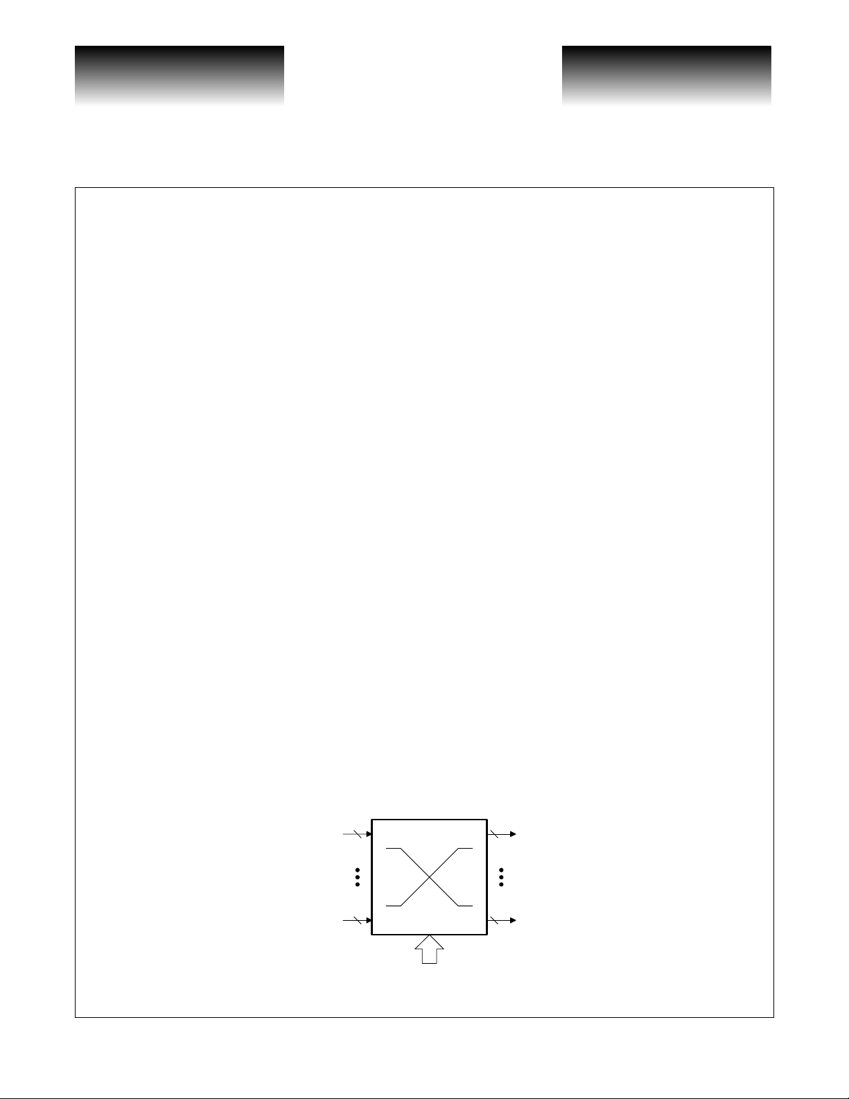
The VSC837 is a monolithic 68x68 asynchronous crosspoint switc h, designed to carry broadband data
streams. The non-blocking switch core is programmed through a triple-mode port interface that allows random
access programming of each input/output port. A high degree of signal integr ity is maintained thr oughout the
chip via fully differential signal paths.
The crosspoint function is based on a multiplexer array architecture. Each data output is driven by a 68:1
multiplexer th at can be prog rammed to one and onl y o ne of its 68 inp uts. The s ignal path is u nregis tered and
fully asynchronous, so there are no restrictions on the phase, frequency, or signal pattern at each input.
Each high-speed output is a fully differential switched current driver with switchable on-die terminations
for maximum signal integrity. Data inputs are terminated on die through 100
plement inputs (see Input Termination section for further detail).
A triple-mode programming interface is provided that allows programming commands to be sent as serial
data or one of two forms of para llel da ta. The input -ref erred mode (b urst mode) allows an input por t to be rout ed
to all outputs in only 4 program cycles. Core program ming can be random for each port addre ss, or multiple
program assignments can be queued and issued simultaneously. The programming may be initialized to a
“straight-through” configuration (A0 to Y0, A1 to Y1, etc.) using the INITB pin.
An activity monitor is provided to allow in-system diagnostics. The activity monitor can observe any highspeed input via an internal 69th multiplexe r.
Unused channels may be powered down to allow efficient use of the switch in appl ications that requi re only
a subset of the channels. Power-down can be accomplished in har dware, via ded icated power pins for pairs of
input and output channels, or in software by programming individual unused outputs with a disable code.
Ω resistors between true and com-
3.2Gb/s
VSC837 Block Diagram
2 2
A0
2
A67
µ
P
control
G52309-0, Rev 3.0 Page 1
02/16/01
© VITESSE SEMICONDUCTOR CORPORATION • 741 Calle Plano • Camarillo, CA 93012
Tel: (800) VITESSE • FAX: (805) 987-5896 • Email: prodinfo@vitesse.com
Internet: www.vitesse.com
Y0
2
Y67
Page 2
VITESSE
SEMICONDUCTOR CORPORATION
3.2Gb/s
68x68 Crosspoint Switch
Functional Block Diagram
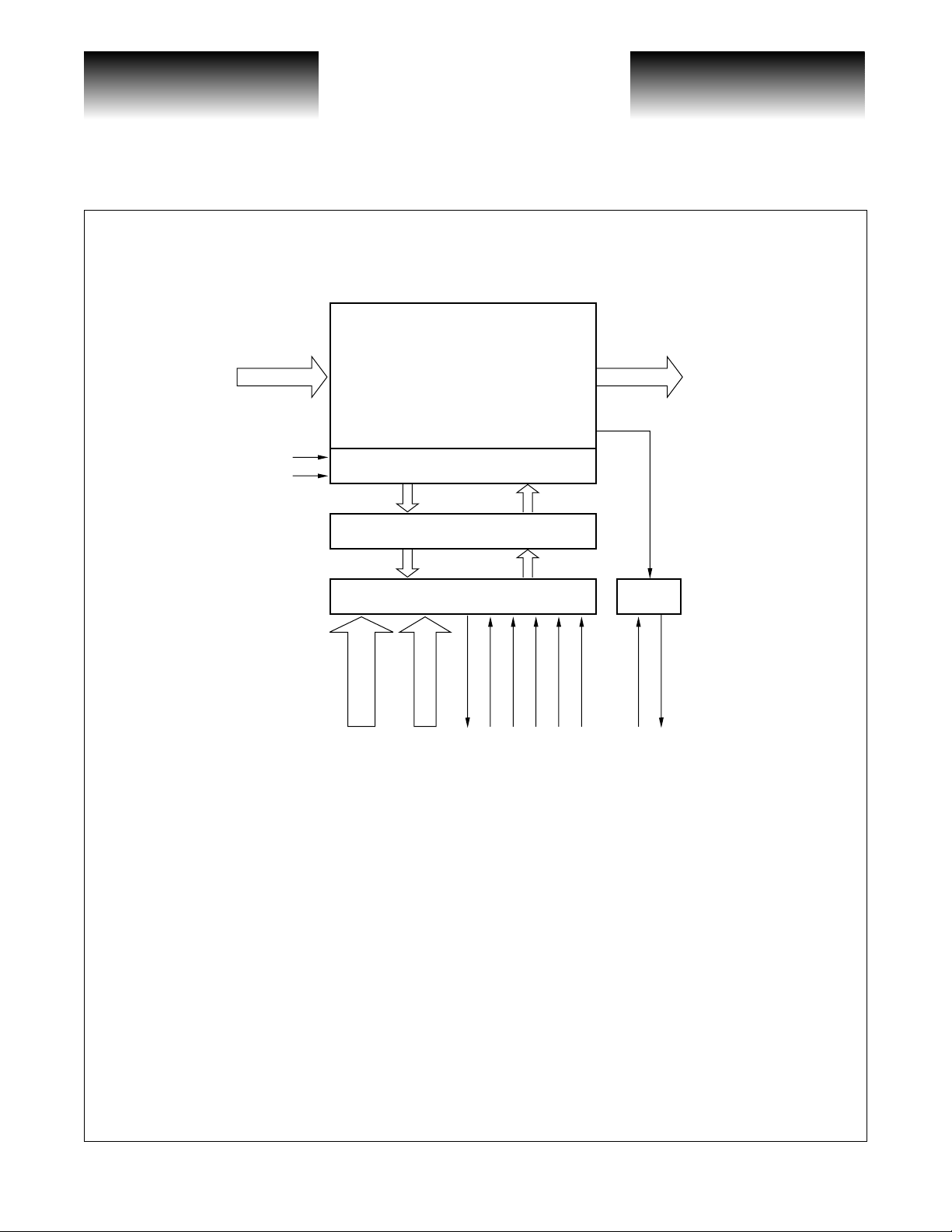
A, AN[0:67]
CONFIG
INITB
68x69 Switch Core
Core Program Registers
Program Memory
Program Interface
Preliminary Data Sheet
VSC837
Y , YN[0:67]
th
Internal 69
Output
Activity
Monitor
CSB
LOAD
BURST
SDOUT
OUTCHAN[18:0]
INCHAN[6:0]
SERIAL
ALE_SCN
ACTCLK
ACTIVITY
Functional Description
Input / Output Characteristics
All input data must be differential and should be nominally biased to +2.0V or AC-coupled. Other levels
are allowed as described under the Input Termination section. On-chip terminations are provided, with a nomi-
nal impedance of 100
coupling.
For direct interconnection of multiple VSC837 devices, a CML termination mode is provided by tying the
ITC pin to V
CC
loads for an open-drain or open-collector differential output.
Data outputs are provided through differential current switches with on-chip back-termination. The output
circuit is capable of dri ving ex ternal 5 0
electronically switchable to enable a power savings of 2W (max) by reducing the output driver current.
Ω differential. All input termination resistors float with an internal bias provided for AC-
, which ties the center point of the 100Ω te rminatio n to VCC, causing the terminat ions to act as
Ω far-end termination (recommended). The output back -terminatio ns are
Page 2 G52309-0, Rev 3.0
© VITESSE SEMICONDUCTOR CORPORATION • 741 Calle Plano • Camarillo, CA 93012
Tel: (800) VITESSE • FAX: (805) 987-5896 • Email: prodinfo@vitesse.com
Internet: www.vitesse.com
02/16/01
Page 3

VITESSE
SEMICONDUCTOR CORPORATION
Preliminary Data Sheet
VSC837
68x68 Crosspoint Switch
Programming Interface
Parallel Mode
In parallel mode (SERIAL=0, BURST=0), the binary word on INCHAN[6:0] is t he numerical identifie r of
the input that will be routed to the specified output. OUTCHAN[6:0] is the numerical identifier of the output
being programmed. A rising edge on the LOAD signal will transfer the programming data to the shadow register in the program me mor y. Raising CONFIG (asynchr onou sly) wi ll t ransf er th e pr og ramm ing data to th e ma in
latches in the program mem ory and cau se the int ernal select signa ls in the core to re-confi gure th e multip lexer.
Lowering CONFIG will latch the main latches. CONFIG may be tied HIGH to enable programming take effect
instantaneously.
This interface may be used with multiplexed address/data buses by using only INCHAN[6:0] without
OUTCHAN[6:0] and dropping ALE when the address of the output to be programmed is present on
INCHAN[6:0]. After the address is latched, the input address may be presented on INCHAN [6:0] and programming proceeds as above.
No read-back capability is provided in parallel mode. Read-back for diagnostic purposes is provided in
serial mode via the scan function.
Serial Mode
In serial mode (SERIAL=1, BURST=0), the INCHAN0 pin becomes the serial data input and the
INCHAN1 pin becomes the serial clock (rising edge triggered). A serial word of the form [Output][Input] is
shifted into the internal shift register, and the LOAD pin is asserted (HIGH) coincident with the last bit of the
data word to signal that the word is to be applied. This transfers the input ident ifier to the shado w register of t he
addressed output. CONFIG is then applied (asynchronously) to transfer one or more program commands to the
main latches of the program memories.
The SDOUT pin follows the data on the INCHAN0_SDIN pin 14 clock cycles later. This enables the user
to chain the serial ports of several crosspoints, shift program data for all switches through such a chain, and
assert LOAD on all switches simultaneously to program all of the connections simultaneously.
The output field is 7 bits long, representing the binary numerical identifier of the output to be programmed.
The input field is 7 bits long, representing the numerical identifier of the input that will be routed to the specified output.
3.2Gb/s
Serial Read-Back
Read-back of the program memor y contents is acco mplished in serial m ode by s etting the ALE_SCN pin
HIGH. This will serially shift out the contents of the main latches in the program memories, slice 68 first and
slice 0 last, and MSB-first, LSB-last for each 7-bit word. One rising edge of INCHAN1_SCLK with
ALE_SCN=0 and SERIAL=1 must occur to load the entire 483-bit shift register prior to shifting out data. At a
clock rate of 66MHz, this operation takes 7.26
G52309-0, Rev 3.0 Page 3
02/16/01
© VITESSE SEMICONDUCTOR CORPORATION • 741 Calle Plano • Camarillo, CA 93012
Tel: (800) VITESSE • FAX: (805) 987-5896 • Email: prodinfo@vitesse.com
µs.
Internet: www.vitesse.com
Page 4

VITESSE
SEMICONDUCTOR CORPORATION
3.2Gb/s
68x68 Crosspoint Switch
Burst Mode
Burst mode programming (BURS T=1, SE RIAL=0) e nabl es an input to be broadcast to any group of 1 t o 17
outputs with a single command. In this mode, rising edges on the LOAD pin will trigger program operations.
The INCHAN[6:0] pins represent the input to be broadcast. The OUTCHAN[18:17] pins represent the page
(quarter) of the program memory to access, and each of the OUTCHA N[16:0] pins represent s 1 of the 17 outputs within that page. A ’1’ on any of those pins will cause that output to be programmed to connect to the input
named on INCHAN[6:0].
No read-back capability is provided in burst mode. See Serial Read-Back section above.
Activity Monitoring
The activity monito r observes the output of the internal 69 th output fro m the core. By p rogrammin g the
69th output to observe various inputs, the input signals can be scanned for activity or lack thereof. Each rising
edge of ACTCLK causes the monitor to read out the act ivity state from t he previous ACT CLK period and cl ears
the internal activity state until a data transition triggers it again. There must be a min imum of o ne ri si ng a nd o ne
falling edge on the observed input data pin during the ACTCLK period for activity to be detected. After poweron the output of ACTIVITY after the first ACTCLK rising edge is unknown.
Selective Power-Down
Unused input and output channels can be made to consume little or no power via one of two methods of
selective power-down.
Preliminary Data Sheet
VSC837
Software Power-Down
Using this feature, unused outputs may be disabled, saving approximately 170 mW per channel for maximum dissipation conditions. This is accomplished by programming each unused output to look at input 127 (7F
Hex), which represents a non-existent input channel. The channel may be subsequently activated by programming a valid input address. It is recommended, however, that any changes in power programming only be executed as part of an initialization sequence to guard against the effects of any switching transients that might
result from changing the power supply current sudden ly. Software mode does not affect the functioning or
power of unused input channels.
Hardware Power-Down
Using this feature, the power associated with given pairs of inp uts may be shut of f by ty ing the corresponding V
tion conditions. The power associated with give n pairs of outputs, including their c ontribution to the core
power, can be shut off by tying the corresponding V
output pair is saved under the maximum dissipation conditions.
ing inputs and outputs will always be on and consuming power. See Figure 6 and Table 10 for the location of
these pins.
pin to VCC (see Table 10). Approximately 160 mW per input pair is saved under t he max imum di ssipa-
EE
pin to VCC (see Table 10). Approximately 360 mW per
EE
Certain V
pins must always be active. In oth er words, t ied to t he most ne gative supp ly, so the correspond-
EE
Page 4 G52309-0, Rev 3.0
© VITESSE SEMICONDUCTOR CORPORATION • 741 Calle Plano • Camarillo, CA 93012
Tel: (800) VITESSE • FAX: (805) 987-5896 • Email: prodinfo@vitesse.com
Internet: www.vitesse.com
02/16/01
Page 5
VITESSE
SEMICONDUCTOR CORPORATION
Preliminary Data Sheet
VSC837
68x68 Crosspoint Switch
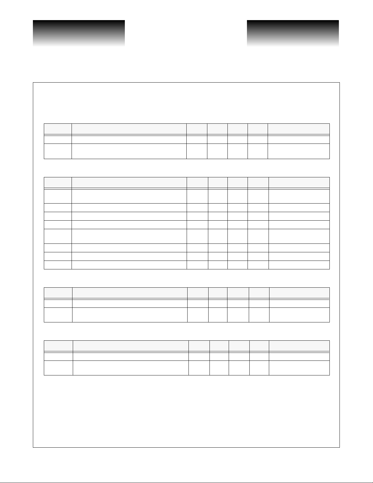
AC Characteristics
Table 1: Data Path
Symbol Parameter Min Typ Max Units
f
RATE
t
SKW
t
PDAY
, t
t
R
, t
t
R
t
JR
t
JP
NOTES:(1) Tested on a sample basis only. (2) Br oadband (unfiltered) deterministic jitter added to a jitter-free input, 223-1 PRBS data pattern.
T a ble 2: Program Interface Timing
Symbol Parameter Min Typ Max Units
t
sWRB
t
hWRB
t
pwLW
t
sCSB
t
hCSB
t
pwCFG
t
sSDIN
t
hSDIN
t
perSCLK
t
sLOAD
t
hLOAD
t
sSERIAL
t
hSERIAL
t
sBURST
t
hBURST
t
dsDOUT
t
pwINITB
t
sSCAN
t
hSCAN
Maximum Data Rate ——3.2 Gb/s
Channel-to-channel delay skew — 300 — ps
Propagation Delay from an A input to a Y output — 750 — ps
High-speed input rise/fall times, 20% to 80% ——150 ps
F
High-speed outpu t rise/fall times, 20% to 80% ——150 ps
F
Output added delay jitter, rms
Output added delay jitter, peak-to-peak
Setup time from INCHAN[6:0] or OUTCHAN[6:0] to rising edge of WRB 3.35 ——ns
Hold time from rising edge of WRB to INCHAN[6:0] or OUTCHAN[6:0] 1.45 ——ns
Pulse width (HIGH or LOW) on LOAD 6.75 ——ns
Setup time from CSB to falling edge of LOAD or ALE_SCN in parallel or burst
mode, or rising edge of LOAD in serial mode.
Hold time of CSB rising edge after LOAD or ALE_SCN rising in parallel or
burst mode, or falling edge of LOAD in serial mode, or falling edge of CONFIG
in any mode.
Pulse width (HIGH or LOW) on CONFIG 6.75 ——ns
Setup time from INCHAN0_SDIN to INCHAN1_SCLK rising 1.65 ——ns
Hold time of INCHAN0_SDIN after INCHAN1_SCLK rising 1.0 —— ns
Minimum period of S CLK in serial mode 15 —— ns
Setup time from LOAD to INCHAN1_SCLK rising 1.85 ——ns
Hold time of LOAD after INCHAN1_SCLK rising 0.95 ——ns
Setup time from SERIAL rising to INCHAN1_SCLK rising when entering serial
mode or SERIAL falling to LOAD falling when entering parallel mode or
SERIAL falling to LOAD rising when entering burst mode.
Hold time from INCHAN1_SCLK rising to SERIAL falling when exiting serial
mode.
Setup time from BURST rising to LOAD rising when entering burst mode or
BURST falling to LOAD falling when entering parallel mode.
Hold time from LOAD rising to BURST falling when exiting burst mode. 2.45 —— ns
Delay from INCHAN1_SCLK rising to SDOUT, 20pF load. ——6.20 ns
Pulse width (HIGH or LOW) on INITB 6.75 ——ns
Setup time from ALE_SCN to INCHAN1_SCLK rising when starting or
completing a serial read-back sequence.
Hold time of ALE_SCN after INCHAN1_SCLK rising when starting or
completing a serial read-back sequence.
(1, 2)
(1, 2)
——10 ps
——40 ps
0 —— ns
0 —— ns
0.90 —— ns
0 —— ns
1.85 —— ns
1.65 —— ns
1.0 —— ns
3.2Gb/s
G52309-0, Rev 3.0 Page 5
02/16/01
© VITESSE SEMICONDUCTOR CORPORATION • 741 Calle Plano • Camarillo, CA 93012
Tel: (800) VITESSE • FAX: (805) 987-5896 • Email: prodinfo@vitesse.com
Internet: www.vitesse.com
Page 6
VITESSE
SEMICONDUCTOR CORPORATION
3.2Gb/s
68x68 Crosspoint Switch
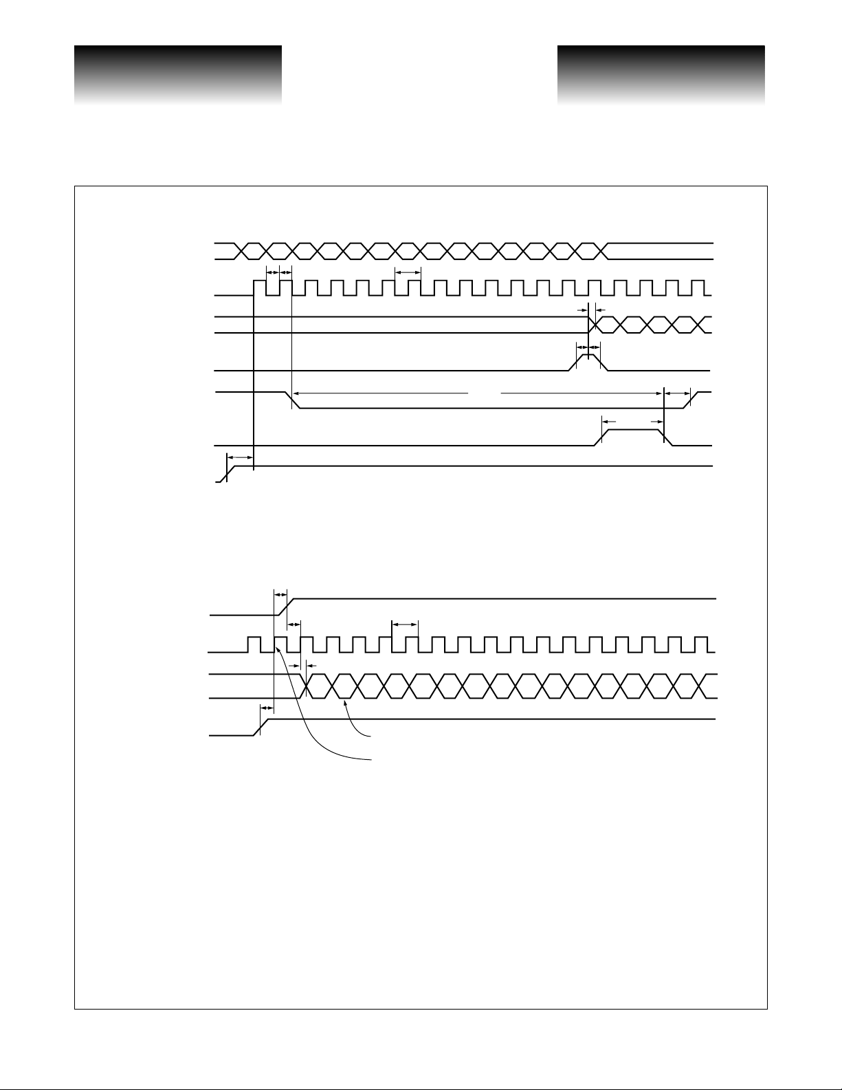
Figure 1: Parallel Mode—Separate Address/Data (leave ALE_SCN pin HIGH)
OUTCHAN[6:0]
INCHAN[6:0]
LOAD
t
sCSB
CSB
CONFIG
t
sSERIAL
SERIAL
INCHAN[6:0]
ALE_SCN
LOAD
CSB
CONFIG
Preliminary Data Sheet
Output Address
Input Address
t
sWRB
t
pwLW
Figure 2: Parallel Mode—Multiplexed Address/Data
Output Address Input Address
t
sCSB
t
hWRB
t
sWRB
t
pwLW
t
hWRB
t
pwCFG
t
pwCFG
VSC837
t
hCSB
t
hCSB
t
SERIAL
sSERIAL
Figure 3: Burst Mode
OUTCHAN[18:17]
OUTCHAN[16:0]
INCHAN[6:0]
LOAD
CSB
CONFIG
BURST
Page 6 G52309-0, Rev 3.0
Output Page Output Page
Output ID Bits Output ID Bits
Input Address Input Address
t
sWRB
t
sCSBtpwLW
t
sBURST
© VITESSE SEMICONDUCTOR CORPORATION • 741 Calle Plano • Camarillo, CA 93012
Tel: (800) VITESSE • FAX: (805) 987-5896 • Email: prodinfo@vitesse.com
t
hWRB
Internet: www.vitesse.com
t
hBURST
t
pwCFG
t
hCSB
02/16/01
Page 7
VITESSE
SEMICONDUCTOR CORPORATION
Preliminary Data Sheet
VSC837
Figure 4: Serial Mode (leave ALE_SCN pin LOW during programming)
INCHAN0_SDIN
INCHAN1_SCLK
SDOUT
LOAD
CSB
CONFIG
SERIAL
O6 O5 O4 O3 O2 O1 O0 I6 I5 I4 I3
t
sSDIN
t
sSERIAL
O(n) = Output Address Bit (n), I(n) = Input Address Bit (n)
t
hSDIN
t
perSCLK
t
sCSB
I2 I1 I0
t
sLOAD
3.2Gb/s
68x68 Crosspoint Switch
t
dsDOUT
O6 O5 O4 O3
t
hLOAD
t
hCSB
t
pwCFG
ALE_SCN
INCHAN1_SCLK
SDOUT
SERIAL
t
sSERIAL
t
hSCAN
Figure 5: Serial Read-Back
t
sSCAN
t
dsDOUT
68 68 68 68 68 68 68 67 67 67 67 67 67 67
B6 B5 B4 B3 B2 B1 B0 B6 B5 B4 B3 B2 B1 B0
MSB of program memory for output 68
Read-back shift register (483 bits long) is loaded here
on rising edge of INCHAN1_SCLK with SERIAL HIGH
and ALE_SCN LOW
t
perSCLK
66
B6
G52309-0, Rev 3.0 Page 7
02/16/01
© VITESSE SEMICONDUCTOR CORPORATION • 741 Calle Plano • Camarillo, CA 93012
Tel: (800) VITESSE • FAX: (805) 987-5896 • Email: prodinfo@vitesse.com
Internet: www.vitesse.com
Page 8
VITESSE
SEMICONDUCTOR CORPORATION
3.2Gb/s
Preliminary Data Sheet
68x68 Crosspoint Switch
DC Characteristics
All characteristics are over the specified operating conditions.
Table 3: Power Supply Requirements
Symbol Parameter Min Typ Max Units Conditions
I
CC
P
T
Table 4: Control Port Input Levels (TTL/CMOS)
Symbol Parameter Min Typ Max Units Conditions
V
IH
V
IL
I
IH
I
IL
V
OH
V
OL
V
OHPU
V
OLPU
VCC supply current 5600 6095 mA
Total chip power (with I
terminations ON, high drive)
Input HIGH voltage 1.7
Input LOW voltage 0 0.8 V
Input HIGH current TBD µA
Input LOW current TBD µA
Output HIGH voltage
Output LOW voltage 0 0.2 V DC load < 2mA
VOH with external pull-up 2.4 V 250Ω to 3.3V(5%)
VOL with external pull-up 0.4 V 250Ω to 3.3V(5%)
TERM
= 0 and back-
VCC-
0.2
13 16 W
VCC+
1.0
V
CC
V
V DC load < 500µA
VSC837
Table 5: Signal Input Levels (high-speed signal path)
Symbol Parameter Min Typ Max Units Conditions
V
IN
V
ICM
Table 6: Signal Output Levels (high-speed signal path)
Input voltage amplitude 150 1100 mV See Note 1
V
Input common-mode voltage
CC
0.7
-
V
-
CC
0.2
VSee Note 2
TERM_CTRL=ON, DRIVE_CTRL=HI
Symbol Parameter Min Typ Max Units Conditions
V
OUT
V
OCM
NOTES: (1) Mean peak-to-peak amplitude measurement of either true or complement of the differential signal. (2) VCC = V
Page 8 G52309-0, Rev 3.0
Output differe nti al vo lta g e 400 600 mV See Note 1, 3
Output common-mode voltage
(3) Terminated in 50
Ω to V
© VITESSE SEMICONDUCTOR CORPORATION • 741 Calle Plano • Camarillo, CA 93012
VCC-
0.3
. This termination is used for testing the part, but other termin ations are allowed—see Table 9.
CC
Tel: (800) VITESSE • FAX: (805) 987-5896 • Email: prodinfo@vitesse.com
Internet: www.vitesse.com
VCC-
0.2
V See Note 2, 3
= 2.5V, VEE = 0V.
CCP
02/16/01
Page 9

VITESSE
SEMICONDUCTOR CORPORATION
Preliminary Data Sheet
VSC837
68x68 Crosspoint Switch
I/O Equivalent Circuits
ITC
PAD
5050
H/S Input Equivalent Circuit
VCC
PAD
PAD PAD
H/S Output Equivalent Circuit
TERM_CTRL
5050
DRIVE_CTRL
Input Termination
The high-speed inputs of the VSC837 are internally terminated by a 100Ω resistor between true and complement inputs. Termination resistors are isolated from each other on-chip. The termination will self-bias to
+2.0V (nominal) for AC-coupled applications. The ITC pin enables direct interconnection of multiple VSC837
devices. With ITC tied to V
minations to act as loads for an open-drain or open-collector differential output.
, the center point of the 10 0Ω te rmin ation resisto r is ti ed to VCC, causing the ter-
CC
3.2Gb/s
Table 7: Allowed Input Termination Schemes
Type Description Comments
1 AC-coupled input
2 DC-coupled from open-drain CML Tie ITC HIGH, terminations acts as 50Ω load to V
3 DC-coupled from back-terminated 2.5V CML Tie ITC HIGH, terminations act s as 50Ω load to V
4 DC-coupled from back-terminated 2.5V CML
5 DC-coupled from back-terminat ed 3.3V LV-PECL Tie ITC LOW, 100Ω differential termination
Tie IT C LOW, 100Ω differential input termination,
input self-biased
Tie IT C LOW, 100Ω differential termination
(preferred over Type 3)
Some allowed termination schemes result in additional ICC current and power dissipation on-chip. See
Table 8.
Table 8: Additional Current and Power
Symbol Description Min Typ Max Units Conditions
I
CC-C
P
CC-C
Additional ICC current when receiving DC-Coupled
CML (ITC = HIGH)
Additional power dissipated on-chip for DC
terminating CML at inputs
680 mA
0.340 W
CC
CC
G52309-0, Rev 3.0 Page 9
02/16/01
© VITESSE SEMICONDUCTOR CORPORATION • 741 Calle Plano • Camarillo, CA 93012
Tel: (800) VITESSE • FAX: (805) 987-5896 • Email: prodinfo@vitesse.com
Internet: www.vitesse.com
Page 10

VITESSE
SEMICONDUCTOR CORPORATION
3.2Gb/s
68x68 Crosspoint Switch
Preliminary Data Sheet
VSC837
Output Termination
The high-speed outputs of the VSC837 are internally back terminated by 50Ω to VCC when the
TERM_CTRL pin is HIGH. When this pin is LOW, the output driver functions as an open-drain CML driver.
Setting DRIVE_CTRL LOW (GND) saves 2W under maximum power dissipation conditions. See Table 9 for
allowable types of terminations and modes of operation.
Table 9: Allowed High-Speed Output Terminations and Modes of Operation
(1)
V
Type Description
1 AC-Coupled to 50Ω termination to any voltage VCC (HIGH) VCC (ON) 500 2.0
2 AC-Coupled to
3 DC-Coupled, terminated in 50Ω to VCC at far-end only GND (LOW) GND (OFF) 500 2.25
4 DC-Coupled, terminated in
5 DC-Coupled, source and far-end terminated in
6 DC-Coupled, source and far-end terminated in 50Ω to V
7 DC-Coupled,
8 DC-Coupled,
NOTE: (1) Measured at output of VSC837, with VCC = 2.5V.
100Ω differential terminat io n V
50Ω to V
at far-end only VCC (HIGH) GND (OFF) 1000 2.0
CC
50Ω to V
100Ω differential termination GND (LOW) V
100Ω differential termination V
DRIVE_
CTRL
(HIGH) VCC (ON) 500 2.0
CC
GND (LOW) VCC (ON) 250 2.375
CC
VCC (HIGH) VCC (ON) 500 2.25
CC
(HIGH) VCC (ON) 500 2.0
CC
TERM_
CTRL
(ON) 250 2.25
CC
OD
(mV)
typ
V
OCM
(V)
typ
(1)
Absolute Maximum Ratings
(1)
Power Supply Voltage (VCC) Potential to GND................................................................................-0.5V to +4.V
TTL Input Vo ltage Applied .....................................................................................................-0.5V to V
ECL Input Vo ltage Applied ....................................................................................................-0.5V to V
Output Current (I
Case Temperature Under Bias (T
Storage Temperature (T
NOTE: (1) Caution: Stresses listed under “Absolute Maximum Ratings” may be applied to devices one at a time without causing perma-
nent damage. Functionality at or exceeding the values listed is not implied. Exposure to these values for extended periods may
affect device reliability.
).................................................................................................................................... 50mA
OUT
).............................................................................................-55oC to + 125oC
C
) ........................................................................................................-65oC to + 150oC
STG
CC
CC
+1.0V
+0.5V
Operating Conditions
Supply Voltage (VEE)..........................................................................................................................................0V
Supply Voltage (V
Supply Voltage (V
Case Temperature Operating Range (T).............................................................................................. 0
) ............................................................................................................................+2.5V ±5%
CC
)...........................................................................................................................+2.5V ±5%
CCP
o
C to 85oC
Page 10 G52309-0, Rev 3.0
© VITESSE SEMICONDUCTOR CORPORATION • 741 Calle Plano • Camarillo, CA 93012
Tel: (800) VITESSE • FAX: (805) 987-5896 • Email: prodinfo@vitesse.com
Internet: www.vitesse.com
02/16/01
Page 11

VITESSE
SEMICONDUCTOR CORPORATION
Preliminary Data Sheet
VSC837
Package Pin Descriptions
27 26 25 24 23 22 21 20 19 18 17 16 15 14 13 12 11 10 9 8
2829
OUTCHAN15
OUTCHAN16
0
4
81216
20 24 28 32
36
40
44
48
52 56 60 64
ITC
LOAD
CONFIG
INCHAN5
OUTCHAN10
OUTCHAN11
OUTCHAN14
OUTCHAN13
OUTCHAN12
OUTCHAN18
OUTCHAN17
2
6 101418
22 26 30
34
38
42
46
50 54 58 62
66
INCHAN6
ALE_SCN
INCHAN1_SCLK
INCHAN0_SDIN
INCHAN4
2
40
Outputs [Yn, YNn]
INCHAN2
3
INCHAN3
1579131721
Figure 6: Pinout Diagram—Bottom View
18 22
26 30
34 38
146
10
8121620
Inputs [An, ANn]
11 15 19 23
42 46 50 54
24 28
32 36
40 44 48
VCC
Dedicated VEE
Common VEE (always On)
control port
Inputs [An, ANn]
27 31 35 39 43
25 29 33 37
47
41 45 49
51 55
58
56 6052
59 63
57 6153
62
68x68 Crosspoint Switch
654321
7
OUTCHAN5
OUTCHAN6
66
OUTCHAN9
OUTCHAN8
OUTCHAN7
64
67
65
Outputs [Yn, YNn]
SERIAL
CSB
SDOUT
BURST
INITB
OUTCHAN2
1 5 9 13 17 21 25 29 33 37
41 45 49
53 57 61
65
TERM_CTRL
OUTCHAN3
DRIVE_CTRL
OUTCHAN4
CMV
OUTCHAN1
3 7 11 15 19 23 27 31 35 39
43 47
51 55 59 63
67
ACTCLK
OUTCHAN0
Ball grid
index
A
B
C
D
E
F
G
H
J
K
L
M
N
P
R
T
U
V
W
Y
AA
AB
AC
AD
ACTIVITY
AE
AF
AG
AH
AJ
3.2Gb/s
G52309-0, Rev 3.0 Page 11
02/16/01
© VITESSE SEMICONDUCTOR CORPORATION • 741 Calle Plano • Camarillo, CA 93012
Tel: (800) VITESSE • FAX: (805) 987-5896 • Email: prodinfo@vitesse.com
Internet: www.vitesse.com
Page 12
VITESSE
SEMICONDUCTOR CORPORATION
3.2Gb/s
Preliminary Data Sheet
68x68 Crosspoint Switch
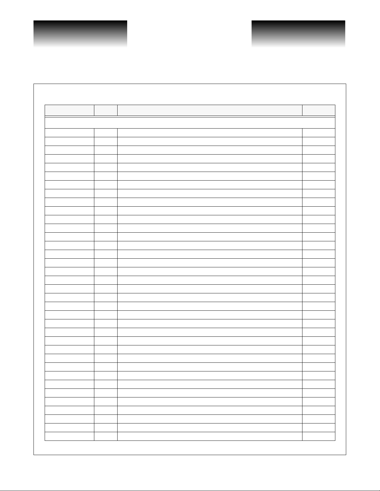
Table 10: Package Pin Identifications
Signal Name Pin Function Level
High-Speed Data Inputs
A0 D23 High-Speed Data Input Channel 0, True PECL
A1 AH23 High-Speed Data Input Channel 1, True PECL
A2 B23 High-Speed Data Input Channel 2, True PECL
A3 AF23 High-Speed Data Input Channel 3, True PECL
A4 D22 High-Speed Data Input Channel 4, True PECL
A5 AH22 High-Speed Data Input Channel 5, True PECL
A6 B22 High-Speed Data Input Channel 6, True PECL
A7 AF22 High-Speed Data Input Channel 7, True PECL
A8 D21 High-Speed Data Input Channel 8, True PECL
A9 AH21 High-Speed Data Input Channel 9, True PECL
A10 B21 High-Speed Data Input Channel 10, True PECL
A11 AF21 High-Speed Data Input Channel 11, True PECL
A12 D20 High-Speed Data Input Channel 12, True PECL
A13 AH20 High-Speed Data Input Channel 13, True PECL
A14 B20 High-Speed Data Input Channel 14, True PECL
A15 AF20 High-Speed Data Input Channel 15, True PECL
A16 D19 High-Speed Data Input Channel 16, True PECL
A17 AH19 High-Speed Data Input Channel 17, True PECL
A18 B19 High-Speed Data Input Channel 18, True PECL
A19 AF19 High-Speed Data Input Channel 19, True PECL
A20 D18 High-Speed Data Input Channel 20, True PECL
A21 AH18 High-Speed Data Input Channel 21, True PECL
A22 B18 High-Speed Data Input Channel 22, True PECL
A23 AF18 High-Speed Data Input Channel 23, True PECL
A24 D17 High-Speed Data Input Channel 24, True PECL
A25 AH17 High-Speed Data Input Channel 25, True PECL
A26 B17 High-Speed Data Input Channel 26, True PECL
A27 AF17 High-Speed Data Input Channel 27, True PECL
A28 D16 High-Speed Data Input Channel 28, True PECL
A29 AH16 High-Speed Data Input Channel 29, True PECL
A30 B16 High-Speed Data Input Channel 30, True PECL
A31 AF16 High-Speed Data Input Channel 31, True PECL
A32 D15 High-Speed Data Input Channel 32, True PECL
A33 AH15 High-Speed Data Input Channel 33, True PECL
A34 B15 High-Speed Data Input Channel 34, True PECL
A35 AF15 High-Speed Data Input Channel 35, True PECL
VSC837
Page 12 G52309-0, Rev 3.0
© VITESSE SEMICONDUCTOR CORPORATION • 741 Calle Plano • Camarillo, CA 93012
Tel: (800) VITESSE • FAX: (805) 987-5896 • Email: prodinfo@vitesse.com
Internet: www.vitesse.com
02/16/01
Page 13

VITESSE
SEMICONDUCTOR CORPORATION
Preliminary Data Sheet
VSC837
Signal Name Pin Function Level
A36 D14 High-Speed Data Input Channel 36, True PECL
A37 AH14 High-Speed Data Input Channel 37, True PECL
A38 B14 High-Speed Data Input Channel 38, True PECL
A39 AF14 High-Speed Data Input Channel 39, True PECL
A40 D13 High-Speed Data Input Channel 40, True PECL
A41 AH13 High-Speed Data Input Channel 41, True PECL
A42 B13 High-Speed Data Input Channel 42, True PECL
A43 AF13 High-Speed Data Input Channel 43, True PECL
A44 D12 High-Speed Data Input Channel 44, True PECL
A45 AH12 High-Speed Data Input Channel 45, True PECL
A46 B12 High-Speed Data Input Channel 46, True PECL
A47 AF12 High-Speed Data Input Channel 47, True PECL
A48 D11 High-Speed Data Input Channel 48, True PECL
A49 AH11 High-Speed Data Input Channel 49, True PECL
A50 B11 High-Speed Data Input Channel 50, True PECL
A51 AF11 High-Speed Data Input Channel 51, True PECL
A52 D10 High-Speed Data Input Channel 52, True PECL
A53 AH10 High-Speed Data Input Channel 53, True PECL
A54 B10 High-Speed Data Input Channel 54, True PECL
A55 AF10 High-Speed Data Input Channel 55, True PECL
A56 D9 High-Speed Data Input Channel 56, True PECL
A57 AH9 High-Speed Data Input Channel 57, True PECL
A58 B9 High-Speed Data Input Channel 58, True PECL
A59 AF9 High-Speed Data Input Channel 59, True PECL
A60 D8 High-Speed Data Input Channel 60, True PECL
A61 AH8 High-Speed Data Input Channel 61, True PECL
A62 B8 High-Speed Data Input Channel 62, True PECL
A63 AF8 High-Speed Data Input Channel 63, True PECL
A64 D7 High-Speed Data Input Channel 64, True PECL
A65 AH7 High-Speed Data Input Channel 65, True PECL
A66 B7 High-Speed Data Input Channel 66 True PECL
A67 AF7 High-Speed Data Input Channel 67, True PECL
AN0 E23 High-Speed Data Input Channel 0, Complement PECL
AN1 AJ23 High-Speed Data Input Channel 1, Complement PECL
AN2 A23 High-Speed Data Input Channel 2, Complement PECL
AN3 AE23 High-Speed Data Input Channel 3, Complement PECL
AN4 E22 High-Speed Data Input Channel 4, Complement PECL
AN5 AJ22 High-Speed Data Input Channel 5, Complement PECL
AN6 A22 High-Speed Data Input Channel 6, Complement PECL
68x68 Crosspoint Switch
3.2Gb/s
G52309-0, Rev 3.0 Page 13
02/16/01
© VITESSE SEMICONDUCTOR CORPORATION • 741 Calle Plano • Camarillo, CA 93012
Tel: (800) VITESSE • FAX: (805) 987-5896 • Email: prodinfo@vitesse.com
Internet: www.vitesse.com
Page 14
VITESSE
SEMICONDUCTOR CORPORATION
3.2Gb/s
Preliminary Data Sheet
68x68 Crosspoint Switch
Signal Name Pin Function Level
AN7 AE22 High-Speed Data Input Channel 7, Complement PECL
AN8 E21 High-Speed Data Input Channel 8, Complement PECL
AN9 AJ21 High-Speed Data Input Channel 9, Complement PECL
AN10 A21 High-Speed Data Input Channel 10, Complement PECL
AN11 AE21 High-Speed Data Input Chann el 11, Complement PECL
AN12 E20 High-Speed Data Input Channel 12, Complement PECL
AN13 AJ20 High-Speed Data Input Channel 13, Complement PECL
AN14 A20 High-Speed Data Input Channel 14, Complement PECL
AN15 AE20 High-Speed Data Input Channel 15, Comp le ment PECL
AN16 E19 High-Speed Data Input Channel 16, Complement PECL
AN17 AJ19 High-Speed Data Input Channel 17, Complement PECL
AN18 A19 High-Speed Data Input Channel 18, Complement PECL
AN19 AE19 High-Speed Data Input Channel 19, Comp le ment PECL
AN20 E18 High-Speed Data Input Channel 20, Complement PECL
AN21 AJ18 High-Speed Data Input Channel 21, Complement PECL
AN22 A18 High-Speed Data Input Channel 22, Complement PECL
AN23 AE18 High-Speed Data Input Channel 23, Comp le ment PECL
AN24 E17 High-Speed Data Input Channel 24, Complement PECL
AN25 AJ17 High-Speed Data Input Channel 25, Complement PECL
AN26 A17 High-Speed Data Input Channel 26, Complement PECL
AN27 AE17 High-Speed Data Input Channel 27, Comp le ment PECL
AN28 E16 High-Speed Data Input Channel 28, Complement PECL
AN29 AJ16 High-Speed Data Input Channel 29, Complement PECL
AN30 A16 High-Speed Data Input Channel 30, Complement PECL
AN31 AE16 High-Speed Data Input Channel 31, Comp le ment PECL
AN32 E15 High-Speed Data Input Channel 32, Complement PECL
AN33 AJ15 High-Speed Data Input Channel 33, Complement PECL
AN34 A15 High-Speed Data Input Channel 34, Complement PECL
AN35 AE15 High-Speed Data Input Channel 35, Comp le ment PECL
AN36 E14 High-Speed Data Input Channel 36, Complement PECL
AN37 AJ14 High-Speed Data Input Channel 37, Complement PECL
AN38 A14 High-Speed Data Input Channel 38, Complement PECL
AN39 AE14 High-Speed Data Input Channel 39, Comp le ment PECL
AN40 E13 High-Speed Data Input Channel 40, Complement PECL
AN41 AJ13 High-Speed Data Input Channel 41, Complement PECL
AN42 A13 High-Speed Data Input Channel 42, Complement PECL
AN43 AE13 High-Speed Data Input Channel 43, Comp le ment PECL
AN44 E12 High-Speed Data Input Channel 44, Complement PECL
AN45 AJ12 High-Speed Data Input Channel 45, Complement PECL
VSC837
Page 14 G52309-0, Rev 3.0
© VITESSE SEMICONDUCTOR CORPORATION • 741 Calle Plano • Camarillo, CA 93012
Tel: (800) VITESSE • FAX: (805) 987-5896 • Email: prodinfo@vitesse.com
Internet: www.vitesse.com
02/16/01
Page 15

VITESSE
SEMICONDUCTOR CORPORATION
Preliminary Data Sheet
VSC837
Signal Name Pin Function Level
AN46 A12 High-Speed Data Input Channel 46, Complement PECL
AN47 AE12 High-Speed Data Input Channel 47, Comp le ment PECL
AN48 E11 High-Speed Data Input Channel 48, Complement PECL
AN49 AJ11 High-Speed Data Input Channel 49, Complement PECL
AN50 A11 High-Speed Data Input Channel 50, Complement PECL
AN51 AE11 High-Speed Data Input Channel 51, Complement PECL
AN52 E10 High-Speed Data Input Channel 52, Complement PECL
AN53 AJ10 High-Speed Data Input Channel 53, Complement PECL
AN54 A10 High-Speed Data Input Channel 54, Complement PECL
AN55 AE10 High-Speed Data Input Channel 55, Comp le ment PECL
AN56 E9 High-Speed Data Input Channel 56, Complement PECL
AN57 AJ9 High-Speed Data Input Channel 57, Complement PECL
AN58 A9 High-Speed Data Input Channel 58, Complement PECL
AN59 AE9 High-Speed Data Input Channel 59, Complement PECL
AN60 E8 High-Speed Data Input Channel 60, Complement PECL
AN61 AJ8 High-Speed Data Input Channel 61, Complement PECL
AN62 A8 High-Speed Data Input Channel 62, Complement PECL
AN63 AE8 High-Speed Data Input Channel 63, Complement PECL
AN64 E7 High-Speed Data Input Channel 64, Complement PECL
AN65 AJ7 High-Speed Data Input Channel 65, Complement PECL
AN66 A7 High-Speed Data Input Channel 66, Complement PECL
AN67 AE7 High-Speed Data Input Channel 67, Complement PECL
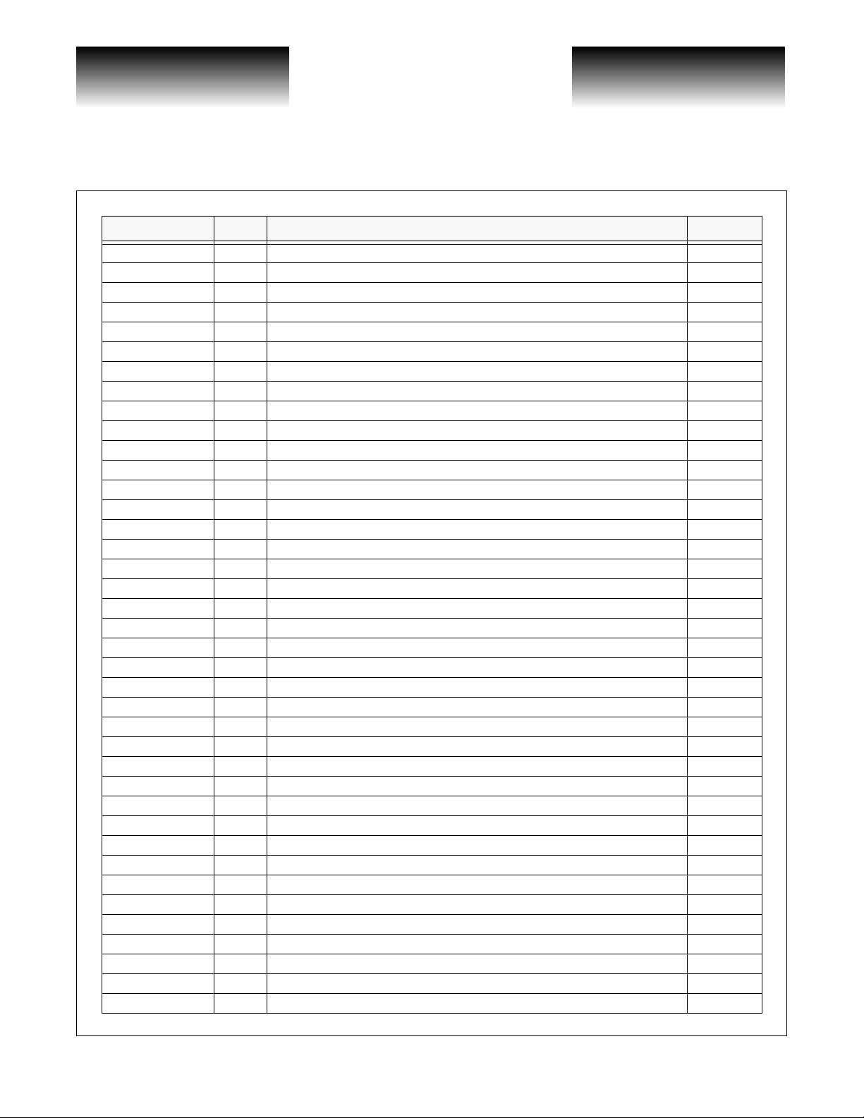
High-Speed Data Outputs
Y0 G28 High-Speed Data Output Channel 0, True CML
Y1 G4 High-Speed Data Output Channel 1, True CML
Y2 G26 High-Speed Data Output Channel 2, True CML
Y3 G2 High-Speed Data Output Channel 3, True CML
Y4 H28 High-Speed Data Output Channel 4, True CML
Y5 H4 High-Speed Data Output Channel 5, True CML
Y6 H26 High-Speed Data Output Channel 6, True CML
Y7 H2 High-Speed Data Output Channel 7, True CML
Y8 J28 High-Speed Data Output Channel 8, True CML
Y9 J4 High-Speed Data Output Channel 9, True CML
Y10 J26 High-Speed Data Output Channel 10, True CML
Y11 J2 High-Speed Data Output Channel 11, True CML
Y12 K28 High-Speed Data Output Channel 12, True CML
Y13 K4 High-Speed Data Output Channel 13, True CML
Y14 K26 High-Speed Data Output Channel 14, True CML
Y15 K2 High-Speed Data Output Channel 15, True CML
68x68 Crosspoint Switch
3.2Gb/s
G52309-0, Rev 3.0 Page 15
02/16/01
© VITESSE SEMICONDUCTOR CORPORATION • 741 Calle Plano • Camarillo, CA 93012
Tel: (800) VITESSE • FAX: (805) 987-5896 • Email: prodinfo@vitesse.com
Internet: www.vitesse.com
Page 16

VITESSE
SEMICONDUCTOR CORPORATION
3.2Gb/s
Preliminary Data Sheet
68x68 Crosspoint Switch
Signal Name Pin Function Level
Y16 L28 High-Speed Data Output Channel 16, True CML
Y17 L4 High-Speed Data Output Channel 17, True CML
Y18 L26 High-Speed Data Output Channel 18, True CML
Y19 L2 High-Speed Data Output Channel 19, True CML
Y20 M28 High-Speed Data Output Channel 20, True CML
Y21 M4 High-Speed Data Output Channel 21, True CML
Y22 M26 High-S peed Data Output Channel 22, True CML
Y23 M2 High-Speed Data Output Channel 23, True CML
Y24 N28 High-Speed Data Output Channel 24, True CML
Y25 N4 High-Speed Data Output Channel 25, True CML
Y26 N26 High-Speed Data Output Channel 26, True CML
Y27 N2 High-Speed Data Output Channel 27, True CML
Y28 P28 High-Speed Data Output Channel 28, True CML
Y29 P4 High-Speed Data Output Channel 29, True CML
Y30 P26 High-Speed Data Output Channel 30, True CML
Y31 P2 High-Speed Data Output Channel 31, True CML
Y32 R28 High-Speed Data Output Channel 32, True CML
Y33 R4 High-Speed Data Output Channel 33, True CML
Y34 R26 High-Speed Data Output Channel 34, True CML
Y35 R2 High-Speed Data Output Channel 35, True CML
Y36 T28 High-Speed Data Output Channel 36, True CML
Y37 T4 High-Speed Data Output Channel 37, True CML
Y38 T26 High-Speed Data Output Channel 38, True CML
Y39 T2 High-Speed Data Output Channel 39, True CML
Y40 U28 High-Speed Data Output Channel 40, True CML
Y41 U4 High-Speed Data Output Channel 41, True CML
Y42 U26 High-Speed Data Output Channel 42, True CML
Y43 U2 High-Speed Data Output Channel 43, True CML
Y44 V28 High-Speed Data Output Channel 44, True CML
Y45 V4 High-Speed Data Output Channel 45, True CML
Y46 V26 High-Speed Data Output Channel 46, True CML
Y47 V2 High-Speed Data Output Channel 47, True CML
Y48 W28 High-Speed Data Output Channel 48, True CML
Y49 W4 H igh-Speed Data Output Channel 49, True CML
Y50 W26 High-Speed Data Output Channel 50, True CML
Y51 W2 H igh-Speed Data Output Channel 51, True CML
Y52 Y28 High-Speed Data Output Channel 52, True CML
Y53 Y4 High-Speed Data Output Channel 53, True CML
Y54 Y26 High-Speed Data Output Channel 54, True CML
VSC837
Page 16 G52309-0, Rev 3.0
© VITESSE SEMICONDUCTOR CORPORATION • 741 Calle Plano • Camarillo, CA 93012
Tel: (800) VITESSE • FAX: (805) 987-5896 • Email: prodinfo@vitesse.com
Internet: www.vitesse.com
02/16/01
Page 17

VITESSE
SEMICONDUCTOR CORPORATION
Preliminary Data Sheet
VSC837
Signal Name Pin Function Level
Y55 Y2 High-Speed Data Output Channel 55, True CML
Y56 AA28 High-Speed Data Outp ut Channel 56, True CM L
Y57 AA4 High-Speed Data Output Channel 57, True CML
Y58 AA26 High-Speed Data Output Channel 58, True C ML
Y59 AA2 High-Speed Data Output Channel 59, True CML
Y60 AB28 High- Speed Data Output C hannel 60, True CML
Y61 AB4 High-Speed Data Output Channel 61, True CML
Y62 AB26 High- Speed Data Output C hannel 62, True CML
Y63 AB2 High-Speed Data Output Channel 63, True CML
Y64 AC28 High- Speed Data Output C hannel 64, True CML
Y65 AC4 High-Speed Data Output Channel 65, True CML
Y66 AC26 High- Speed Data Output C hannel 66, True CML
Y67 AC2 High-Speed Data Output Channel 67, True CML
YN0 G29 High-Speed Data Output Channel 0, Complement CML
YN1 G5 High-Speed Data Output Channel 1, Complement CML
YN2 G25 High-Speed Data Output Channel 2, Complement CML
YN3 G1 High-Speed Data Output Channel 3, Complement CML
YN4 H29 High-Speed Data Output Channel 4, Complement CML
YN5 H5 High-Speed Data Output Channel 5, Complement CML
YN6 H25 High-Speed Data Output Channel 6, Complement CML
YN7 H1 High-Speed Data Output Channel 7, Complement CML
YN8 J29 High -Sp eed Data Output Channel 8, Complement CML
YN9 J5 High-Speed Data Output Chan nel 9, Complement CM L
YN10 J25 High-Speed Data Output Channel 10, Complement CML
YN11 J1 High-Speed Data Output Channel 11, Complement CML
YN12 K29 High-Speed Data Output Channel 12, Complement CML
YN13 K5 High-Speed Data Output Channe l 1 3, Complement CML
YN14 K25 High-Speed Data Output Channel 14, Complement CML
YN15 K1 High-Speed Data Output Channe l 1 5, Complement CML
YN16 L29 High-Speed Data Output Channel 16, Complement CML
YN17 L5 High-Speed Data Output Channel 17, Complement CML
YN18 L25 High-Speed Data Output Channel 18, Complement CML
YN19 L1 High-Speed Data Output Channel 19, Complement CML
YN20 M29 High-Speed Data Output Channel 20, Complement CML
YN21 M5 High-Speed Data Output Channel 21, Complement CML
YN22 M25 High-Speed Data Output Channel 22, Complement CML
YN23 M1 High-Speed Data Output Channel 23, Complement CML
YN24 N29 High-Speed Data Output Channel 24, Complement CML
YN25 N5 High-Speed Data Output Channe l 2 5, Complement CML
68x68 Crosspoint Switch
3.2Gb/s
G52309-0, Rev 3.0 Page 17
02/16/01
© VITESSE SEMICONDUCTOR CORPORATION • 741 Calle Plano • Camarillo, CA 93012
Tel: (800) VITESSE • FAX: (805) 987-5896 • Email: prodinfo@vitesse.com
Internet: www.vitesse.com
Page 18

VITESSE
SEMICONDUCTOR CORPORATION
3.2Gb/s
Preliminary Data Sheet
68x68 Crosspoint Switch
Signal Name Pin Function Level
YN26 N25 High-Speed Data Output Channel 26, Complement CML
YN27 N1 High-Speed Data Output Channe l 2 7, Complement CML
YN28 P29 High-Speed Data Output Channel 28, Complement CML
YN29 P5 High-Speed Data Output Channel 29, Complement CML
YN30 P25 High-Speed Data Output Channel 30, Complement CML
YN31 P1 High-Speed Data Output Channel 31, Complement CML
YN32 R29 High-Spee d Data Output Channel 32, Complement CML
YN33 R5 High-Speed Data Output Channel 33, Complement CML
YN34 R25 High-Spee d Data Output Channel 34, Complement CML
YN35 R1 High-Speed Data Output Channel 35, Complement CML
YN36 T29 High-Speed Data Output Channel 36, Complement CML
YN37 T5 High-Speed Data Output Channel 37, Complement CML
YN38 T25 High-Speed Data Output Channel 38, Complement CML
YN39 T1 High-Speed Data Output Channel 39, Complement CML
YN40 U29 High-Speed Data Output Channel 40, Complement CML
YN41 U5 High-Speed Data Output Channe l 4 1, Complement CML
YN42 U25 High-Speed Data Output Channel 42, Complement CML
YN43 U1 High-Speed Data Output Channe l 4 3, Complement CML
YN44 V29 High-Speed Data Output Channel 44, Complement CML
YN45 V5 High-Speed Data Output Channe l 4 5, Complement CML
YN46 V25 High-Speed Data Output Channel 46, Complement CML
YN47 V1 High-Speed Data Output Channe l 4 7, Complement CML
YN48 W29 High-Speed Data Output Channel 48, Complement CML
YN49 W5 High-Speed Data Output Channel 49, Complement CML
YN50 W25 High-Speed Data Output Channel 50, Complement CML
YN51 W1 High-Speed Data Output Channel 51, Complement CML
YN52 Y29 High-Speed Data Output Channel 52, Complement CML
YN53 Y5 High-Speed Data Output Channe l 5 3, Complement CML
YN54 Y25 High-Speed Data Output Channel 54, Complement CML
YN55 Y1 High-Speed Data Output Channe l 5 5, Complement CML
YN56 AA29 High-Speed Data Output Channel 56, Complement CML
YN57 AA5 High-Speed Data Output Channel 57, Complement CML
YN58 AA25 High-Speed Data Output Channel 58, Complement CML
YN59 AA1 High-Speed Data Output Channel 59, Complement CML
YN60 AB29 High-Speed Data Output Channel 60, Complement CML
YN61 AB5 High-Speed Data Output Channel 61, Complement CML
YN62 AB25 High-Speed Data Output Channel 62, Complement CML
YN63 AB1 High-Speed Data Output Channel 63, Complement CML
YN64 AC29 High-Speed Data Output Channel 64, Complement CML
VSC837
Page 18 G52309-0, Rev 3.0
© VITESSE SEMICONDUCTOR CORPORATION • 741 Calle Plano • Camarillo, CA 93012
Tel: (800) VITESSE • FAX: (805) 987-5896 • Email: prodinfo@vitesse.com
Internet: www.vitesse.com
02/16/01
Page 19

VITESSE
SEMICONDUCTOR CORPORATION
Preliminary Data Sheet
VSC837
Signal Name Pin Function Level
YN65 AC5 High-Speed Data Output Channel 65, Complement CML
YN66 AC25 High-Speed Data Output Channel 66, Complement CML
YN67 AC1 High-Speed Data Output Channel 67, Complement CML
Control Pins
ACTCLK A D2 Clock for Activity Monitor (<10MHz) TTL
ACTIVITY AD1 ActivityResult from Previous ACTCLK Period TTL
ALE_SCN AD25
BURST AH6 Logic HIGH sets Burst Mode TTL
CMV AD3 Output Drive Current Control (leave floating) ANALOG
CONFIG F27 Logic HIGH Transfers Programming to Main Program Memory TTL
CSB AF6 Chip Select (active LOW) TTL
DRIVE_CTRL AD4 Output Drive Current Switch (LOW = 10mA, HIGH = 20mA) TTL
INCHAN0_SDIN AG24 Input Channel, Bit 0 and Serial Data in Serial Mode TTL
INCHAN1_SCLK AF24 Input Channel, Bit 1 and Serial Clock in Serial Mode TTL
INCHAN2 AE24 Input Channel, Bit 2 TTL
INCHAN3 AH24 Input Channel, Bit 3 TTL
INCHAN4 AJ24 Input Channel, Bit 4 TTL
INCHAN5 AD27 Input Channel, Bit 5 TTL
INCHAN6 AD26 Input Channel, Bit 6 TTL
INITB AJ6 INITB=0 Forces “Straight-Through” Program TTL
ITC AD29
LOAD AD28
OUTCHAN0 F1 Output Channel, Bit 0 TTL
OUTCHAN1 F2 Output Channel, Bit 1 TTL
OUTCHAN2 F5 Output Channel, Bit 2 TTL
OUTCHAN3 F4 Output Channel, Bit 3 TTL
OUTCHAN4 F3 Output Channel, Bit 4 TTL
OUTCHAN5 A6 Output Channel, Bit 5 TTL
OUTCHAN6 B6 Output Channel, Bit 6 TTL
OUTCHAN7 E6 Output Channel, Bit 7 (burst mode only) TTL
OUTCHAN8 D6 Output Channel, Bit 8 (burst mode only) TTL
OUTCHAN9 C6 Output Channel, Bit 9 (burst mode only) TTL
OUTCHAN10 A24 Output Channel, Bit 10 (burst mode only) TTL
OUTCHAN11 B24 Output Channel, Bit 11 (burst mode only) TTL
OUTCHAN12 E24 Output Channel, Bit 12 (burst mode only) TTL
OUTCHAN13 D24 Output Channel, Bit 13 (burst mode only) TTL
Address Latch Enable for Multiplexed Parallel Mode; Scan Enable for Serial
Mode. See Figures 2 through 6 for Proper Use.
Input Termination Control (GND = floating input termination,
= CML mode. See Table 7).
V
CC
Rising Edge Writes Data in Parallel and Burst Modes,
See Figure 5 for Serial Mode
68x68 Crosspoint Switch
3.2Gb/s
TTL
ANALOG
TTL
G52309-0, Rev 3.0 Page 19
02/16/01
© VITESSE SEMICONDUCTOR CORPORATION • 741 Calle Plano • Camarillo, CA 93012
Tel: (800) VITESSE • FAX: (805) 987-5896 • Email: prodinfo@vitesse.com
Internet: www.vitesse.com
Page 20

VITESSE
SEMICONDUCTOR CORPORATION
3.2Gb/s
Preliminary Data Sheet
68x68 Crosspoint Switch
Signal Name Pin Function Level
OUTCHAN14 C24 Output Channel, Bit 14 (burst mode only) TTL
OUTCHAN15 F29 Output Channel, Bit 15 (burst mode only) TTL
OUTCHAN16 F28 Output Channel, Bit 16 (burst mode only) TTL
OUTCHAN17 F25 Output Channel, Bit 17 (burst mode only) TTL
OUTCHAN18 F26 Output Channel, Bit 18 (burst mode only) TTL
SDOUT AG6 Serial Data Out for Serial Mode and Scan TTL
SERIAL AE6 SERIAL = 1 Sets Serial Mode TTL
TERM_CTRL AD5
Power Supplies
VEE C23 Common Negative Power Supply GND
VEE C7 Common Negative Power Supply GND
VEE R3 Common Negative Power Supply GND
VEE AG7 Common Negative Power Supply GND
VEE AG23 Common Negative Power Supply GND
VEE R27 Common Negative Power Supply GND
VCC A1 Positive Power Supply 2.5V
VCC A2 Positive Power Supply 2.5V
VCC A3 Positive Power Supply 2.5V
VCC A4 Positive Power Supply 2.5V
VCC A5 Positive Power Supply 2.5V
VCC A25 Positive Power Supply 2.5V
VCC A26 Positive Power Supply 2.5V
VCC A27 Positive Power Supply 2.5V
VCC A28 Positive Power Supply 2.5V
VCC A29 Positive Power Supply 2.5V
VCC AE1 Positive Power Supply 2.5V
VCC AE2 Positive Power Supply 2.5V
VCC AE25 Positive Power Supply 2.5V
VCC AE26 Positive Power Supply 2.5V
VCC AE27 Positive Power Supply 2.5V
VCC AE28 Positive Power Supply 2.5V
VCC AE29 Positive Power Supply 2.5V
VCC AE3 Positive Power Supply 2.5V
VCC AE4 Positive Power Supply 2.5V
VCC AE5 Positive Power Supply 2.5V
VCC AF1 Positive Power Supply 2.5V
VCC AF2 Positive Power Supply 2.5V
VCC AF25 Positive Power Supply 2.5V
Output Back-Termination Control (LOW = no back termination;
HIGH = 50Ω back-termination to V
. See Table 9).
CC
VSC837
TTL
Page 20 G52309-0, Rev 3.0
© VITESSE SEMICONDUCTOR CORPORATION • 741 Calle Plano • Camarillo, CA 93012
Tel: (800) VITESSE • FAX: (805) 987-5896 • Email: prodinfo@vitesse.com
Internet: www.vitesse.com
02/16/01
Page 21

VITESSE
SEMICONDUCTOR CORPORATION
Preliminary Data Sheet
VSC837
Signal Name Pin Function Level
VCC AF26 Positive Power Supply 2.5V
VCC AF27 Positive Power Supply 2.5V
VCC AF28 Positive Power Supply 2.5V
VCC AF29 Positive Power Supply 2.5V
VCC AF3 Positive Power Supply 2.5V
VCC AF4 Positive Power Supply 2.5V
VCC AF5 Positive Power Supply 2.5V
VCC AG1 Positive Power Supply 2.5V
VCC AG2 Positive Power Supply 2.5V
VCC AG25 Positive Power Supply 2.5V
VCC AG26 Positive Power Supply 2.5V
VCC AG27 Positive Power Supply 2.5V
VCC AG28 Positive Power Supply 2.5V
VCC AG29 Positive Power Supply 2.5V
VCC AG3 Positive Power Supply 2.5V
VCC AG4 Positive Power Supply 2.5V
VCC AG5 Positive Power Supply 2.5V
VCC AH1 Positive Power Supply 2.5V
VCC AH2 Positive Power Supply 2.5V
VCC AH25 Positive Power Supply 2.5V
VCC AH26 Positive Power Supply 2.5V
VCC AH27 Positive Power Supply 2.5V
VCC AH28 Positive Power Supply 2.5V
VCC AH29 Positive Power Supply 2.5V
VCC AH3 Positive Power Supply 2.5V
VCC AH4 Positive Power Supply 2.5V
VCC AH5 Positive Power Supply 2.5V
VCC AJ1 Positive Power Supply 2.5V
VCC AJ2 Positive Power Supply 2.5V
VCC AJ25 Positive Power Supply 2.5V
VCC AJ26 Positive Power Supply 2.5V
VCC AJ27 Positive Power Supply 2.5V
VCC AJ28 Positive Power Supply 2.5V
VCC AJ29 Positive Power Supply 2.5V
VCC AJ3 Positive Power Supply 2.5V
VCC AJ4 Positive Power Supply 2.5V
VCC AJ5 Positive Power Supply 2.5V
VCC B1 Positive Power Supply 2.5V
VCC B2 Positive Power Supply 2.5V
68x68 Crosspoint Switch
3.2Gb/s
G52309-0, Rev 3.0 Page 21
02/16/01
© VITESSE SEMICONDUCTOR CORPORATION • 741 Calle Plano • Camarillo, CA 93012
Tel: (800) VITESSE • FAX: (805) 987-5896 • Email: prodinfo@vitesse.com
Internet: www.vitesse.com
Page 22

VITESSE
SEMICONDUCTOR CORPORATION
3.2Gb/s
Preliminary Data Sheet
68x68 Crosspoint Switch
Signal Name Pin Function Level
VCC B25 Positive Power Supply 2.5V
VCC B26 Positive Power Supply 2.5V
VCC B27 Positive Power Supply 2.5V
VCC B28 Positive Power Supply 2.5V
VCC B29 Positive Power Supply 2.5V
VCC B3 Positive Power Supply 2.5V
VCC B4 Positive Power Supply 2.5V
VCC B5 Positive Power Supply 2.5V
VCC C1 Positive Power Supply 2.5V
VCC C2 Positive Power Supply 2.5V
VCC C25 Positive Power Supply 2.5V
VCC C26 Positive Power Supply 2.5V
VCC C27 Positive Power Supply 2.5V
VCC C28 Positive Power Supply 2.5V
VCC C29 Positive Power Supply 2.5V
VCC C3 Positive Power Supply 2.5V
VCC C4 Positive Power Supply 2.5V
VCC C5 Positive Power Supply 2.5V
VCC D1 Positive Power Supply 2.5V
VCC D2 Positive Power Supply 2.5V
VCC D25 Positive Power Supply 2.5V
VCC D26 Positive Power Supply 2.5V
VCC D27 Positive Power Supply 2.5V
VCC D28 Positive Power Supply 2.5V
VCC D29 Positive Power Supply 2.5V
VCC D3 Positive Power Supply 2.5V
VCC D4 Positive Power Supply 2.5V
VCC D5 Positive Power Supply 2.5V
VCC E1 Positive Power Supply 2.5V
VCC E2 Positive Power Supply 2.5V
VCC E25 Positive Power Supply 2.5V
VCC E26 Positive Power Supply 2.5V
VCC E27 Positive Power Supply 2.5V
VCC E28 Positive Power Supply 2.5V
VCC E29 Positive Power Supply 2.5V
VCC E3 Positive Power Supply 2.5V
VCC E4 Positive Power Supply 2.5V
VCC E5 Positive Power Supply 2.5V
VEEP_T1 C22 Negative Power Supply for Inputs A4/AN4+A6/AN6 GND
VSC837
Page 22 G52309-0, Rev 3.0
© VITESSE SEMICONDUCTOR CORPORATION • 741 Calle Plano • Camarillo, CA 93012
Tel: (800) VITESSE • FAX: (805) 987-5896 • Email: prodinfo@vitesse.com
Internet: www.vitesse.com
02/16/01
Page 23

VITESSE
SEMICONDUCTOR CORPORATION
Preliminary Data Sheet
VSC837
Signal Name Pin Function Level
VEEP_T2 C21 Negative Power Supply for Inputs A8/AN8+A10/AN10 GND
VEEP_T3 C20 Negative Power Supply for Inputs A12/AN12+A14/AN14 GND
VEEP_T4 C19 Negative Power Supply for Inputs A16/AN16+A18/AN18 GND
VEEP_T5 C18 Negative Power Supply for Inputs A20/AN20+A22/AN22 GND
VEEP_T6 C17 Negative Power Supply for Inputs A24/AN24+A26/AN26 GND
VEEP_T7 C16 Negative Power Supply for Inputs A28/AN28+A30/AN30 GND
VEEP_T8 C15 Negative Power Supply for Inputs A32/AN32+A34/AN34 GND
VEEP_T9 C14 Negative Power Supply for Inputs A36/AN36+A38/AN38 GND
VEEP_T10 C13 Negative Power Supply for Inputs A40/AN40 +A42/AN42 GND
VEEP_T11 C12 Negative Power Supply for Inputs A44/AN44+A46/AN46 GND
VEEP_T12 C11 Negative Power Supply for Inputs A48/AN48 +A50/AN50 GND
VEEP_T13 C10 Negative Power Supply for Inputs A52/AN52 +A54/AN54 GND
VEEP_T14 C9 Negative Power Supply for Inputs A56/AN56+A58/AN58 GND
VEEP_T15 C8 Negative Power Supply for Inputs A60/AN60+A62/AN62 GND
VEEP_B1 AG22 Negative Power Supply for Inputs A5/AN5+A7/AN7 GND
VEEP_B2 AG21 Negative Power Supply for Inputs A9/AN9+A11/AN11 GND
VEEP_B3 AG20 Negative Power Supply for Inputs A13/AN13+A15/AN15 GND
VEEP_B4 AG19 Negative Power Supply for Inputs A17/AN17+A19/AN19 GND
VEEP_B5 AG18 Negative Power Supply for Inputs A21/AN21+A23/AN23 GND
VEEP_B6 AG17 Negative Power Supply for Inputs A25/AN25+A27/AN27 GND
VEEP_B7 AG16 Negative Power Supply for Inputs A29/AN29+A31/AN31 GND
VEEP_B8 AG15 Negative Power Supply for Inputs A33/AN33+A35/AN35 GND
VEEP_B9 AG14 Negative Power Supply for Inputs A37/AN37+A39/AN39 GND
VEEP_B10 AG13 Negative Power Supply for Inputs A41/AN41+A43/AN43 GND
VEEP_B11 AG12 Negative Power Supply for Inputs A45/AN45+A47/AN47 GND
VEEP_B12 AG11 Negative Power Supply for Inputs A49/AN49+A51/AN51 GND
VEEP_B13 AG10 Negative Power Supply for Inputs A53/AN53+A55/AN55 GND
VEEP_B14 AG9 Negative Power Supply for Inputs A57/AN57+A59/AN59 GND
VEEP_B15 AG8 Negative Power Supply for Inputs A61/AN61+A63/AN63 GND
VEEP_L0 G3 Negative Power Supply for Outputs Y1/YN1+Y3/YN3 GND
VEEP_L1 H3 Negative Power Supply for Outputs Y5/YN5+Y7/YN7 GND
VEEP_L2 J3 Negative Power Supply for Outputs Y9/YN9+Y11/YN11 GND
VEEP_L3 K3 Negative Power Supply for Outputs Y13/YN13+Y15/YN15 GND
VEEP_L4 L3 Negative Power Supply for Outputs Y17/YN17+Y19/YN19 GND
VEEP_L5 M3 Negative Power Supply for Outputs Y21/YN21+Y23/YN23 GND
VEEP_L6 N3 Negative Power Supply for Outputs Y25/YN25+Y27/YN27 GND
VEEP_L7 P3 Negative Power Supply for Outputs Y29/YN29+Y31/YN31 GND
VEEP_L9 T3 Negative Power S up ply for Ou tputs Y37/YN37+Y39/YN39 GND
VEEP_L10 U3 Negative Power Supply for Outputs Y41/YN41+Y43/YN43 GND
68x68 Crosspoint Switch
3.2Gb/s
G52309-0, Rev 3.0 Page 23
02/16/01
© VITESSE SEMICONDUCTOR CORPORATION • 741 Calle Plano • Camarillo, CA 93012
Tel: (800) VITESSE • FAX: (805) 987-5896 • Email: prodinfo@vitesse.com
Internet: www.vitesse.com
Page 24

VITESSE
SEMICONDUCTOR CORPORATION
3.2Gb/s
Preliminary Data Sheet
68x68 Crosspoint Switch
Signal Name Pin Function Level
VEEP_L11 V3 Negative Power Supply for Outputs Y45/YN45+Y47/YN47 GND
VEEP_L12 W3 Negative Power Supply for Outputs Y49/YN49+Y51/YN51 GND
VEEP_L13 Y3 Negative Power Supply for Outputs Y53/YN53+Y55/YN55 GND
VEEP_L14 AA3 Negative Power Supply for Outputs Y57/YN57+Y59/YN59 GND
VEEP_L15 AB3 Negative Power Supply for Outputs Y61/YN61+Y6 3/YN63 GND
VEEP_L16 AC3 Negative Power Supply for Outputs Y65/YN65+Y6 7/YN67 GND
VEEP_R0 G27 Negative Power S upply for Outputs Y0/YN0+Y2/YN2 GND
VEEP_R1 H27 Negative Power S upply for Outputs Y4/YN4+Y6/YN6 GND
VEEP_R2 J27 Negative Power Supply for Outputs Y8/YN8+Y10/YN10 GND
VEEP_R3 K27 Negative Power Supply for Outputs Y12/YN12+Y14/YN14 GND
VEEP_R4 L27 Negative Power Supply for Outputs Y16/YN16+Y18/YN18 GND
VEEP_R5 M27 Negative Power Supply for Outputs Y20/YN20+Y22/YN22 GND
VEEP_R6 N27 Negative Power Supply for Outputs Y24/YN24+Y26/YN26 GND
VEEP_R7 P27 Negative Power Supply for Outputs Y28/YN28+Y30/YN30 GND
VEEP_R9 T27 Negative Power Supply for Outputs Y36/YN36+Y38/YN38 GND
VEEP_R10 U27 Negative Power Supply for Outputs Y40/YN40+Y42/YN42 GND
VEEP_R11 V27 Negative Power Supply for Outputs Y44/YN44+Y46/YN46 GND
VEEP_R12 W27 Negative Power Supply for Outputs Y48/YN48+Y50/YN50 GND
VEEP_R13 Y27 Negative Power Supply for Outputs Y52/YN52+Y54/YN54 GND
VEEP_R14 AA27 Negative Power Supply for Outputs Y56/YN56+Y58/YN58 GND
VEEP_R15 AB27 Negative Power Supply for Outputs Y60/YN60+Y62/YN62 GND
VEEP_R16 AC27 Negative Power Supply for Outputs Y64/YN64+Y66/YN66 GND
VSC837
Page 24 G52309-0, Rev 3.0
© VITESSE SEMICONDUCTOR CORPORATION • 741 Calle Plano • Camarillo, CA 93012
Tel: (800) VITESSE • FAX: (805) 987-5896 • Email: prodinfo@vitesse.com
Internet: www.vitesse.com
02/16/01
Page 25

VITESSE
SEMICONDUCTOR CORPORATION
Preliminary Data Sheet
VSC837
Package Information - 37.5mm 480 BGA
3.2Gb/s
68x68 Crosspoint Switch
00.30 S C A S B S
G52309-0, Rev 3.0 Page 25
02/16/01
© VITESSE SEMICONDUCTOR CORPORATION • 741 Calle Plano • Camarillo, CA 93012
Tel: (800) VITESSE • FAX: (805) 987-5896 • Email: prodinfo@vitesse.com
Internet: www.vitesse.com
Page 26

VITESSE
SEMICONDUCTOR CORPORATION
3.2Gb/s
68x68 Crosspoint Switch
Ordering Informatio n
The order number for this product is formed by a combination of the device type and package type.
Device Type
3.2Gb/s 68x68 Crosspoint Switch
VSC837
Preliminary Data Sheet
VSC837
XX
Package Style
UG: 480 TBGA, 37.5mm Body
Notice
Vitesse Semiconductor Corporation (“Vitesse”) provides this document for informational purposes only. This document contains pre-production
information about Vitesse products in their con ce pt , development and/or testing p hase . All i nformation in this document, including descriptions of
features, functions, performan ce, technical specifications and availability, is subject to change wi th out notice at any ti me. Nothing contained in this
document shall be c ons trued as e xten ding an y w arran ty or pr omise , e xp ress or imp lied , th at a ny Vitesse produ ct wi ll b e av ail able as described or
will be suitable for or will accomp lis h any particular task.
Vitesse products are not intended for use in life support applia nc es, devices or systems. Use of a Vitesse product in such applications without written consent is prohibited.
Page 26 G52309-0, Rev 3.0
© VITESSE SEMICONDUCTOR CORPORATION • 741 Calle Plano • Camarillo, CA 93012
Tel: (800) VITESSE • FAX: (805) 987-5896 • Email: prodinfo@vitesse.com
Internet: www.vitesse.com
02/16/01
 Loading...