

Page 1
VITESSE
SEMICONDUCTOR CORPORATION
Datasheet
VSC834
with Input Signal Activity (ISA) Monitoring
2.5Gb/s 17x17 Crosspoin t Switch
Features
• 17 Input by 17 Output Crosspoint Switch
• 2.5Gb/s NRZ Data Bandwidth
• 42 Gb/s Aggregate Bandwidth
• TTL Compatible µP Interface
• Differential PECL Data Inputs
• On-chip 50Ω Input Terminations
• 50Ω Source Terminated PECL Output Drivers
• Single 3.3V Supply
• 9W Maximum Power Dissipation
• High Performance 256 Pin BGA Package
General Description
The VSC834 is a monolithic 17x17 asynchron ous crosspoint switch design ed to carry broadband data
streams at up to 2.5Gb/s. The non-blocking switch core is programmed through a parallel microprocessor interface that allows random access programming of each output port. A high degree of signal integrity is maintained through the chip through fully differential signal paths.
The crosspoint function is based on a mu ltiplexer tr ee architecture . Each data o utput is driven by a 17:1
multiplexer tree that can be programmed to one and only one of its 17 inputs, and each data input can be programmed to multiple outputs. The signal path is unregistered, so no clock is required for the data inputs. The
signal path is asynchronous, so there are no restrictions on the phase, frequency, or signal pattern at each input.
Each input channel has an activity monitor function that can be used to identify loss of activity (LOA). An interrupt pin is provid ed to signal LOA, af ter which an external controller can query the chip to determi ne the channel(s) on which the fault occurred.
Each output driver is a fully differential switched current driver with on-die back-termina tions for maximum signal integrity. Data inputs are terminated on die through 50
The parallel interface uses TTL levels, and provides address, data, and control pins th at are compatible with
a microprocessor-style interface. The control port provides access to all chip functions, including LOA, and
programming. Program buffering is provided to allow multiple program assignments to be queued and issued
simultaneously via a single configure command.
Ω resistors connected to V
TERM
.
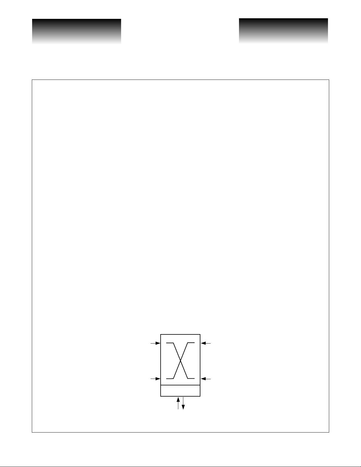
VSC834 Block Diagram
A0
A16
Control Logic
µP Interface
G52247-0, Rev 4.2 Page 1
02/09/01
© VITESSE SEMICONDUCTOR CORPORATION • 741 Calle Plano • Camarillo, CA 93012
Tel: (800) VITESSE • FAX: (805) 987-5896 • Email: prodinfo@vitess e.com
Internet: www.vitesse.com
Y0
Y16
Page 2

VITESSE
SEMICONDUCTOR CORPORATION
2.5Gb/s 17x17 Crosspoint Switch
with Input Signal Activity (ISA) Monitoring
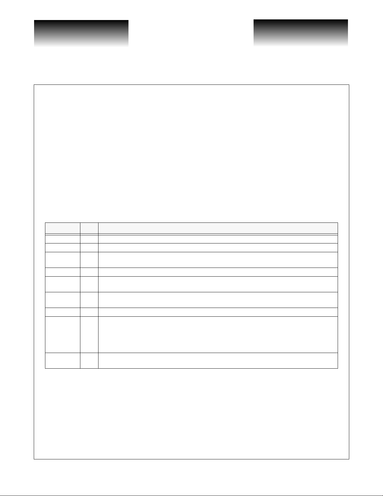
Figure 1: Detailed Block Diagram:
A, AN[16:0]
LOA
Monitor
Switch Core
Program Memory
Control Interface
17x17
17
Datasheet
VSC834
Y , YN[16:0]
Output Drivers
DATA[4:0], ADDR[5:0]
ALE, CSB, WRB, RDB INTB,
MONCLK, CONFIG
Functional Description
Data Paths
All input data must be differential and biased to PECL levels. On-chip terminations are provided, with a
nominal impedance of 50
Data outputs are provided through di fferential current switches with on-chip term inations that produc e a
PECL level output swing. The drive level of the output circuit is designed to produce standard PECL levels
when terminated in 50
age level of the output swing will be shifted from its nominal value. The common-mode voltage of the output
swing can be adjusted using the VCOM pin. The adjustment range is not calibrated, but typically allows for
about +
200mV of adjustment in the output common-mode voltage.
Output channels can be powered off in pairs if fewer than 17 outputs are required. By connecting the VEE
pin associated with a given pair of outputs to V
reduced by roughly 200mW.
Ω. All input termination resistors are tied to V
TERM
.
Ω to 2.0V. Other termination voltages are possible, such as to V
, the output pa irs will pu ll to V
CC
CC
or 1.3V, but the volt-
CC
and chip power will be
Page 2 G52247-0, Rev 4.2
© VITESSE SEMICONDUCTOR CORPORATION • 741 Ca l le Pl an o • Camarillo, CA 93012
Tel: (800) VITESSE • FAX: (805) 987-5896 • Email: prodinfo@vitesse.com
Internet: www.vitesse.com
02/09/01
Page 3
VITESSE
SEMICONDUCTOR CORPORATION
Datasheet
VSC834
Programming Interface
with Input Signal Activity (ISA) Monitoring
2.5Gb/s 17x17 Crosspoin t Switch
The switch core is programmed through a parallel interface circuit that allows random reads or writes to the
program memory array. The program memory array is buffered to allow multiple programming instructions to
be loaded simultaneously with the CONFIG pin. Parallel programing can be clocked at up to a 50MHz rate.
The program data is composed of two parts: output address and input address. The output address, denoted
by ADDR[5:0], specifies which output channel is to be p rogrammed. The input ad dress, denot ed by DAT A[4:0],
specifies which input port the switch slice should connect to. The format of the program data is simple binary,
where the binary value maps directly to the switch slice position and/or input port number. For example:
ADDR[5:0] (000100) / DATA[4:0] (001 10) would di rect output channel Y4 to connect to inpu t channel A6. T he
programming state may be verified (read back) by applying the add ress of the des ired output and asser ting
RDB. The programming state is unknown at power-on. Additional address space is provided for access to the
monitor registers (See Table 2). The microprocessor interface consists of the following signals. Levels are TTL
(see Tab le 6).
Table 1: Signal Table
Pin I/O Description
D[5:0] B Bidirectional data bus to transfer data to/from internal program registers
A[5:0] I Address bus to select internal program registers for read-write operations
ALE I
CSB I Chip Select (Active Low): assert this pin whenever the part is being read or programmed.
WRB I
RDB I
INTB O Interrupt (Active Low): this signal is asserted when an LOA condition is found
CONFIG I
MONCLK I
Address Latch Enable: for use with multiplexed address/data buses. Latches the address bus internally
when low.
Write (Active Low): program data will be transferred to the first level internal registers on the rising
edge of this signal (when CSB is also low).
Read (Active Low): program data from the internal pro gram or monitor re gisters will be read out on the
data bus when this signal goes low (with CSB also low).
Configure (Active High): assert this signal to transfer queued program information from the first-level
internal registers to the second-level registers, making the programming take effect. This signal may be
tied high to leave the second-level registers transparent so all programmi ng will take effect
immediately. CSB must be active (low) when CONFIG is asserted. CONFIG may be tied to a highorder bit of the addr ess bus
Monitor states are transferred to mon itor registers on the rising edge of this signal. MONCLK is not
expected to exceed 3MHz.
Loss of Activity (LOA) Monitoring
The LOA function consists of an activity monitor on each in put channel, conn ected directly to the pads.
The state of a monitor (whether or not it has been toggled by an input transition) can be observed by applying
the address (See Table 2) of the monitor register cor respondi ng to the si gnal of int erest an d assertin g RDB. Each
monitor register is four bits in leng th, covering the state of four inp uts or output s. There is one extra o ne-bit
monitor for each of the 17
th
input and 17th output. The state of each moni t or is t ransferred to the register period-
ically on the rising edge of MONCLK, whereupon the activity monitor is clered until more activity is detected.
G52247-0, Rev 4.2 Page 3
02/09/01
© VITESSE SEMICONDUCTOR CORPORATION • 741 Calle Plano • Camarillo, CA 93012
Tel: (800) VITESSE • FAX: (805) 987-5896 • Email: prodinfo@vitesse.com
Internet: www.vitesse.com
Page 4
VITESSE
SEMICONDUCTOR CORPORATION
2.5Gb/s 17x17 Crosspoint Switch
with Input Signal Activity (ISA) Monitoring
If any change in a monitor state occurs after sampling by MONCLK, an interrupt will be signalled by
asserting INTB, and the user must identify the offending channel by reading the monitor states. The interrup t
will be cleared when the corresponding activity monitor is read, but the monitor state will not be changed. If
multiple monitors have triggered the interrupt, it will persist until all the corresponding monitors have been
read.
The LOA circuitry requires a min imum signal level of 30- 150 mV peak-peak to recognize an input as
active. This is requi r ed to di sti ngu ish noise on an unconnected signal (where both inputs float to the terminat i on
voltage) from activity on a live signal. A minimum of two transitions defines activity. The threshold signal
level can be adjusted with the VHYS pin, which can set the threshold from zero to the maximum allowed input
swing. The VHYS pin will self-bias to a nomial value that will be appropriate for most ap plicati ons (30-150mV
p-p input level). Although uncalibrated for nominal level, gain and linearity, the VHYS pin can be externally
set to adjust the threshold lev el over the entire rang e of the input signal, from z ero to the maximum l evel
allowed at the input.
Table 2: Memory Map
Address Access Description
00h R/W Output Y0’s programmed input channel ( write and then assert CONFIG to program)
01h R/W Output Y1’s programmed input channel
... ... ...
10h R/W Output Y16’s programmed input channel
11h R/W Internal output Y17’s programmed input channel
... ... ...
20h R/W Internal output Y32’s programmed input channel
21h R/O Rx Activity monitor for inputs A0, A1,A2,A3 ( Logic ‘1’=No activity)
22h R/O Rx Activity monitor for inputs A4, A5,A6,A7
23h R/O Rx Activity monitor for inputs A8, A9,A10,A11
24h R/O Rx Activity monitor for inputs A12, A13,A14,A15
25h R/O Rx Activity monitor for input A16
Datasheet
VSC834
Page 4 G52247-0, Rev 4.2
© VITESSE SEMICONDUCTOR CORPORATION • 741 Ca l le Pl an o • Camarillo, CA 93012
Tel: (800) VITESSE • FAX: (805) 987-5896 • Email: prodinfo@vitesse.com
Internet: www.vitesse.com
02/09/01
Page 5
VITESSE
SEMICONDUCTOR CORPORATION
Datasheet
VSC834
with Input Signal Activity (ISA) Monitoring
2.5Gb/s 17x17 Crosspoin t Switch
AC Characteristics
Table 3: Data Path
Parameter Description Min Typ Max Units
F
RATE
T
ISKW
T
OSKW
tR, t
F
, t
t
R
F
t
jP
Note: Unless otherwise stated, all specifications are guaranteed but not tested.
Note 1: Skew between any two input channels to a given output.
Note 2: Skew between any two output channels from the same input channel.
Note 3: Required for high-speed output rise/fall spec at F
Note 4: Broadband jitter added to a jitter-free signal; jitter is primarily in the form of ISI for random data
Data rate - - 2.5 Gb/s
Input channel delay skew (1) - 300 - ps
Output channel delay skew (2) - 300 - ps
High-speed input rise/fall times, 20% to 80% (3) - - 150 ps
High-speed output rise/fall times, 20% to 80% - - 150 ps
Output data eye jitter, peak-peak, 223 PRBS (4) - - 100 ps
=2.5 Gbits/s. For lower rate signals, use 0.375/F
RATE
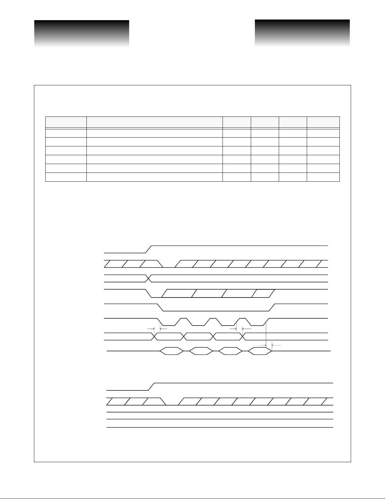
Figure 2: Interrupt Timing (Change in Monitor State Registers)
RATE
MONCLK
Monitor State
Monitor State Reg
INTB
CSB
RDB
ADDR[5:0]
DATA[4:0]
Figure 3: Interrupt Timing (No Change in Monitor State Registers)
MONCLK
Monitor State
Monitor State Reg
T
sRDB
T
hRDB
T
tsDATA
INTB
G52247-0, Rev 4.2 Page 5
02/09/01
© VITESSE SEMICONDUCTOR CORPORATION • 741 Calle Plano • Camarillo, CA 93012
Tel: (800) VITESSE • FAX: (805) 987-5896 • Email: prodinfo@vitesse.com
Internet: www.vitesse.com
Page 6

VITESSE
SEMICONDUCTOR CORPORATION
2.5Gb/s 17x17 Crosspoint Switch
with Input Signal Activity (ISA) Monitoring
Figure 4: Program Timing
ADDR[5:0]
DATA[4:0]
CSB
T
sCSB
T
sWRB
T
hWRB
WRB
RDB
CONFIG
Table 4: Programing Port Interface Timing
Parameter Description Min Max Units
T
config
T
pdADDR
T
pdRDB
T
pdint
T
pdstate
T
sRDB
T
hRDB
T
sWRB
T
hWRB
T
sCONFIG
T
sCSB
T
pwCONFIG
T
pwWRB
T
pwRDB
T
tsDATA
T
sALE
Note 1: Measured from falling edge.
Note 2: Measured from rising edge.
Switch configuration delay - 6 ns
Data read propagation delay from ADDR - 30 ns
Data read propagation delay from RDB (1) - 7 ns
Interrupt propagation delay from MONCLK (2) - 50 ns
MONCLK to internal state register change delay (2) - 6 ns
ADDR to RDB setup time 5 - ns
RDB to ADDR hold time 3 - ns
WRB setup time (for either ADDR or DATA ) 5 - ns
WRB hold time (for either ADDR or DATA) 3 - ns
WRB to CONFIG setup time 1 - ns
CSB setup time (to either WRB or RDB) 0 - ns
CONFIG pulse width (high) 10 - ns
WRB pulse width (low an d hig h) 10 - ns
RDB pulse width (low an d high) 10 - ns
DATA tri-state delay (from either RDB or CSB) (2) - 10 ns
ALE setup time (for multiplexed ADDR/DATA bus) 5 - ns
T
sCONFIG
Datasheet
VSC834
Page 6 G52247-0, Rev 4.2
© VITESSE SEMICONDUCTOR CORPORATION • 741 Ca l le Pl an o • Camarillo, CA 93012
Tel: (800) VITESSE • FAX: (805) 987-5896 • Email: prodinfo@vitesse.com
Internet: www.vitesse.com
02/09/01
Page 7

VITESSE
SEMICONDUCTOR CORPORATION
Datasheet
VSC834
with Input Signal Activity (ISA) Monitoring
2.5Gb/s 17x17 Crosspoin t Switch
DC Characteristics (All Characteristics Are Over The Specified Operating Conditions)
Table 5: Power
Parameter Description Min Typ Max Units Conditions
I
CC
P
T
I
TERM-V
I
TERM-E
Note: ICC Specified with outputs terminated with 50Ω to +2.0V and Chip V
Table 6: Control Port Input Levels
Parameter Description Min Typ Max Units Conditions
V
VCOM
V
VHYS
V
IH
V
IL
I
IH
I
IL
I
OZ
VCC supply current 2600 mA
Total chip power (VCC = 3.45V and +85ºC
case)
V
supply current wit h V
TERM
V
supply current wit h V
TERM
VCOM bias voltage (L and R ) 2.0 V VCC=3.3V
VHYS bias voltage 1.65 V VCC=3.3V
Input HIGH voltage (TTL) 2.0 — 3.5 V —
Input LOW voltage (TTL) 0 — 0.8 V —
Input HIGH current (TTL) ——500 µAVIN = 2.4V
Input LOW current (TTL) ——-500 µAVIN = 0.5V
Tristate output current (TTL) -100 — 100 µAV
TERM =VCC
TERM =VCC
-1.3V ~0 mA
-2.0V -600 mA
=+2.0V.
TERM
9W
OUT
= 0.4V-2.4V
Table 7: Data Input Levels (Differential PECL)
Parameter Description Min Typ Max Units Conditions
V
ID
V
ICM
Input differential voltage 200 — 1000 mV —
Input common-mode voltage 1.8 — 2.2 V VCC=3.3V
Table 8: Data Output Levels (Differential PECL)
Parameter Description Min Typ Max Units Conditions
V
OD
V
OCM
NOTE: (1) Nominal PECL mode, VCC=V
Output differential voltage 600 — 1000 mV Note 1
Output common-mode voltage 1.8 — 2.2 V Note 1
=3.3V, VEE=0, terminated 50Ω to +2.0V.
CCP
G52247-0, Rev 4.2 Page 7
02/09/01
© VITESSE SEMICONDUCTOR CORPORATION • 741 Calle Plano • Camarillo, CA 93012
Tel: (800) VITESSE • FAX: (805) 987-5896 • Email: prodinfo@vitesse.com
Internet: www.vitesse.com
Page 8

VITESSE
SEMICONDUCTOR CORPORATION
2.5Gb/s 17x17 Crosspoint Switch
with Input Signal Activity (ISA) Monitoring
Datasheet
VSC834
Absolute Maximum Ratings
Power Supply Voltage (VCC) Potential to GND ............................................................................-0.5 V to +4.0 V
TTL Input Voltage Applied ..................................................................................................-0.5 V to V
ECL Input Voltage Applied ..................................................................................................-0.5 V to V
Output Current (I
Input Current (I
V
Case Temperature Under Bias (T
Storage Temperature (T
Note: Caution: Stresses listed under “Absolute Maximum Ratings” may be applied to devices one at a time without causing per-
Current (I
TERM
manent damage. Functionality at or exceeding the values listed is not implied. Exposure to these values for extended periods may affect device reliability.
)................................................................................................................................... 50 mA
OUT
) ......................................................................................................................................±50 mA
IN
) ............................................................................................................................±800 mA
TERM
).............................................................................................-55oC to + 125oC
C
) .......................................................................................................-65oC to + 150oC
STG
CC
CC
Operating Conditions
Supply voltage (VEE) .........................................................................................................................................0 V
Supply voltage (V
Supply voltage (V
Termination voltage (V
Case Temperature Operating Range (T).............................................................................................. 0
Junction Temperature Operating Range (T
).............................................................................................................................+3.3V ±5%
CC
) ...........................................................................................................................+3.3V ±5%
CCP
)..................................................................................................................VCC -1.3V
TERM
o
C to 85oC
) .................................................................................... 0oC to 110oC
J
+0.5 V
+0.5 V
ESD Ratings
Proper ESD procedures should be used when handling this product. The VSC834 is rated to the following
ESD voltages based on the human body model:
1. All pins are rated at or above 1000V.
Page 8 G52247-0, Rev 4.2
© VITESSE SEMICONDUCTOR CORPORATION • 741 Ca l le Pl an o • Camarillo, CA 93012
Tel: (800) VITESSE • FAX: (805) 987-5896 • Email: prodinfo@vitesse.com
Internet: www.vitesse.com
02/09/01
Page 9

VITESSE
SEMICONDUCTOR CORPORATION
Datasheet
VSC834
I/O Equivalent Circuits
V
CCVTERM
Pad
PECL Input Equivalent Circuit
V
CC
50Ω
V
CC
2.5Gb/s 17x17 Crosspoin t Switch
with Input Signal Activity (ISA) Monitoring
V
CC
SIG
15Ω
V
CC
50Ω
Pad
i
SIG
V
CC
V
CC
Pad
V
CC
50Ω
i
PECL Output Equivalent Circuit
V
CC
Pad
V
COM
Equivalent Circuit
V
EE
(L or R) Input
1.3kΩ
(On-die bias network) (On-die bias network)
2kΩ
Pad
V
Equivalent Circuit
(C or L) Input
HYS
25kΩ
5kΩ
5kΩ
V
EE
G52247-0, Rev 4.2 Page 9
02/09/01
© VITESSE SEMICONDUCTOR CORPORATION • 741 Calle Plano • Camarillo, CA 93012
Tel: (800) VITESSE • FAX: (805) 987-5896 • Email: prodinfo@vitesse.com
Internet: www.vitesse.com
Page 10

VITESSE
SEMICONDUCTOR CORPORATION
2.5Gb/s 17x17 Crosspoint Switch
with Input Signal Activity (ISA) Monitoring
Datasheet
VSC834
Package Pin Descriptions
The VSC834 is packaged in a 27x27mm 256 pin ball grid array package. The 256 BGA package is thermally enhanced and carries the high-speed signals over controlled impedanc e lines from the solder ball to the
circuit die. The following sections describe the pinout and mechanical details of the VSC834.
Figure 5: Functional Pinout Floorplan
Programming
Interface
Y0
A0 A2 A4
I/P LOA and Termination Control Logic
17:1 Switch Slice Pair
A16
Y2
Y16
17:1 Switch Slice Pair
17:1 Switch Slice Pair
17:1 Switch Slice Pair
17:1 Switch Slice Pair
17:1 Switch Slice Pair
I/P LOA and Termination
A1
A3 A5
Y1
Y3
Y15
Control Logic
A15 Programming
Interface
Page 10 G52247-0, Rev 4.2
© VITESSE SEMICONDUCTOR CORPORATION • 741 Ca l le Pl an o • Camarillo, CA 93012
Tel: (800) VITESSE • FAX: (805) 987-5896 • Email: prodinfo@vitesse.com
Internet: www.vitesse.com
02/09/01
Page 11

VITESSE
SEMICONDUCTOR CORPORATION
Datasheet
VSC834
Y2
Y0
Y4
A0
with Input Signal Activity (ISA) Monitoring
Figure 6: Pinout Diagram
A8A4A2
VCC
VEE
A12
ADR0
ADR2
A16
A14A10
ADR1
A6
2.5Gb/s 17x17 Crosspoin t Switch
BALL
1
ALE
ADR3
ADR4
ADR5
234567891011121314151617181920
MONCLK
Y3
Y1
GRID
INDEX
A
B
C
D
E
F
G
H
Y8
Y14
Y6
Y10
Y12
Y16
VCOML
A1
A3
VTERM
BOTT OM VIEW
A5 A9
A11 A15
A7
A13
D2
INTB
D1 D0
D3
D4D5
WRB CSB
Y5
Y9
Y11
Y15
VCOMRVHYS
CONFIGRDB
J
Y7
K
L
M
N
Y13
P
R
T
U
V
W
Y
G52247-0, Rev 4.2 Page 11
02/09/01
© VITESSE SEMICONDUCTOR CORPORATION • 741 Calle Plano • Camarillo, CA 93012
Tel: (800) VITESSE • FAX: (805) 987-5896 • Email: prodinfo@vitesse.com
Internet: www.vitesse.com
Page 12

VITESSE
SEMICONDUCTOR CORPORATION
2.5Gb/s 17x17 Crosspoint Switch
with Input Signal Activity (ISA) Monitoring
Table 9: Pin Identification
Signal
Name
A0, NA0 A15, A14 Data Input PECL
A1, NA1 Y15, Y14 Data Input PECL
A2, NA2 D14, C14 Data Input PECL
A3, NA3 U14, V14 Data Input PECL
A4, NA4 C13, D13 Data Input PECL
A5, NA5 V13, U13 Data Input PECL
A6, NA6 A13, A12 Data Input PECL
A7, NA7 Y13, Y12 Data Input PECL
A8, NA8 D12, C12 Data Input PECL
A9, NA9 U12, V12 Data Input PECL
A10, NA10 C11, D11 Data Input PECL
A11, NA11 V11, U11 Data Input PECL
A12, NA12 A11, A10 Data Input PECL
A13, NA13 Y11, Y10 Data Input PECL
A14, NA14 D10, C10 Data Input PECL
A15, NA15 U10, V10 Data Input PECL
A16, NA16 C9, D9 Data Input PECL
Y0, YN0 G18, G17 Data Output PECL
Y1, YN1 G1, H1 Data Output PECL
Y2, YN2 G20, H20 Data Output PECL
Y3, YN3 H4, H3 Data Output PECL
Y4, YN4 H17, H18 Data Output PECL
Y5, YN5 J3, J4 Data Output PECL
Y6, YN6 J18, J17 Data Output PECL
Y7, YN7 J1, K1 Data Output PECL
Y8, YN8 L20, M20 Data Output PECL
Y9, YN9 M4, M3 Data Output PECL
Y10, YN10 M1 7, M1 8 Data Output PECL
Y11, YN11 N3, N4 Data Output PECL
Y12, YN12 N18, N17 Data Output PECL
Y13, YN13 N1, P1 Data Output PECL
Y14, YN14 N20, P20 Data Output PECL
Y15, YN15 P4, P3 Data Output PECL
Pin Function Level
High Speed Data Inputs
High Speed Data Outputs
Datasheet
VSC834
Page 12 G52247-0, Rev 4.2
© VITESSE SEMICONDUCTOR CORPORATION • 741 Ca l le Pl an o • Camarillo, CA 93012
Tel: (800) VITESSE • FAX: (805) 987-5896 • Email: prodinfo@vitesse.com
Internet: www.vitesse.com
02/09/01
Page 13

VITESSE
SEMICONDUCTOR CORPORATION
Datasheet
VSC834
with Input Signal Activity (ISA) Monitoring
2.5Gb/s 17x17 Crosspoin t Switch
Table 9: Pin Identification
Signal
Name
Y16, YN16 P17, P18 Data Output PECL
Pin Function Level
Programming Port
ADR0 B8 Program data address TTL
ADR1 D8 Program data address TTL
ADR2 C8 Program data address TTL
ADR3 B7 Program data address TTL
ADR4 C7 Program data address TTL
ADR5 D7 Program data address TTL
D0 V7 Program data TTL
D1 V8 Program data TTL
D2 U8 Program data TTL
D3 W8 Program data TTL
D4 Y8 Program data TTL
D5 Y9 Program data TTL
ALE A7 Address latch enable (active high) TTL
INTB U7 Interrupt (active low) TTL
RDB W7 Read enable (active low) TTL
WRB Y7 Write enable (active low) TTL
CONFIG W6 Configuration strobe (active high) TTL
CSB Y6 C hip sele c t (active low) TTL
MONCLK A6 Loss of activity mo ni tor clock (active high) TTL
Power Supplies
A1, A2, A3, A4, A5, A16, A17, A18,
A19, A20, B1, B2, B3, B4, B5, B15, B16,
B17, B18, B19, B20, C1, C2, C3, C4 , C5,
C6, C16, C17, C18, C19, C20, D1, D2,
D3, D4, D5, D16, D17, D18, D19, D20,
E1, E2, E3, E4, E17, E18, E19, E20, F1,
F2, F3, F4, F19, F20, G3, G4, G19, H2,
VCC
J20, K2, K3, K4, K17, K18, K19, K20,
L1, L2, L3, L4, L17, L18, L19, M1, P2,
R1, R2, R4, R17, R18, R20, T1, T2, T3,
T4, T17, T18, T19, T20, U1, U2, U3, U4,
U16, U17, U18, U19, U20, V1, V2, V3,
V4, V16, V17, V18, V19, V20, W1, W2,
W3, W4, W5, W16, W17, W18, W 19,
W20, Y1, Y2, Y3, Y4, Y5, Y16, Y17,
Y18, Y19, Y20
Power +3.3V
G52247-0, Rev 4.2 Page 13
02/09/01
© VITESSE SEMICONDUCTOR CORPORATION • 741 Calle Plano • Camarillo, CA 93012
Tel: (800) VITESSE • FAX: (805) 987-5896 • Email: prodinfo@vitesse.com
Internet: www.vitesse.com
Page 14

VITESSE
SEMICONDUCTOR CORPORATION
2.5Gb/s 17x17 Crosspoint Switch
with Input Signal Activity (ISA) Monitoring
Table 9: Pin Identification
Signal
Name
A8, A9, B6, B10, B11, B13, B14, C15,
VEE
VEE H19 Power for output channels 0, 2 GND
VEE G2 Power for output channels 1, 3 GND
VEE J19 Power for output channels 4, 6 GND
VEE J2 Power for output channels 5, 7 GND
VEE N19 Power for output channels 8, 10 GND
VEE M2 Power for output channels 9, 11 GND
VEE P19 Power for output channels 12, 14 GND
VEE N2 Power for output channels 13, 15 GND
VEE R19 Power for output channel 16 GND
VTERM B9, B12, F17, W9, W12 Termination power +2.0V
VCOML U15 Slicing level for Y0 - YN16 (even) ANALOG
VCOMR V5 Slicing level for Y1 - YN15 (odd) ANALOG
VHYS V6 Loss of activity hysterisis thresh old ANALOG
D6, D15, F18, M19, R3, U5, U6, U9, V9,
V15, W10, W11, W13, W14, W15
Pin Function Level
Datasheet
VSC834
Power GND
Miscellaneous
Page 14 G52247-0, Rev 4.2
© VITESSE SEMICONDUCTOR CORPORATION • 741 Ca l le Pl an o • Camarillo, CA 93012
Tel: (800) VITESSE • FAX: (805) 987-5896 • Email: prodinfo@vitesse.com
Internet: www.vitesse.com
02/09/01
Page 15

VITESSE
45 DEGREE 0.5MM CHAMFER
SEMICONDUCTOR CORPORATION
Datasheet
VSC834
Package Information
BOTTOM VIEW
17
10
E1
DETAIL B
F
P
19
18
20
2.5Gb/s 17x17 Crosspoin t Switch
with Input Signal Activity (ISA) Monitoring
27mm 256 BGA Package Drawing
g
1112131415
9
8
16
10
1
567
3
2
4
A
C
E
G
J
L
N
R
U
W
e
B
D
F
H
K
M
P
T
V
Y
D1
e
CORNER
DETAIL B
D
g
0.30 S C A S B S
b
0.10 S C
4
0.10
-A-
-B-
11
A1
c
A
ccc
//
C
TOP VIEW
E
-C-
5
aaa C
DIMENSIONAL REFERENCES
REF. MIN.
A
A1
D
0.60
26.80 27.00
D1
E
26.80 27.00
E1
b
c
0.65
1.05
M
N
aaa
ccc
e
P
g
0.15
0.40
F
G52247-0, Rev 4.2 Page 15
02/09/01
NOM. MAX.
1.801.65
0.65
1.95
0.70
27.20
24.13 (BSC.)
27.20
24.13 (BSC.)
0.75
1.15
0.85
1.25
20
256
0.25
0.25
1.27 TYP.
0.50
© VITESSE SEMICONDUCTOR CORPORATION • 741 Calle Plano • Camarillo, CA 93012
Tel: (800) VITESSE • FAX: (805) 987-5896 • Email: prodinfo@vitesse.com
6
NOTES:
1. ALL DIMENSIONS ARE IN MILLIMETERS.
2. "e" REPRESENTS THE BASIC SOLDER BALL GRID PITCH.
3. "M" REPRESENTS THE BASIC SOLDER BALL MATRIX SIZE,
AND SYMBOL "N" IS THE MAXIMUM ALLOWABLE NUMBER OF
BALLS AFTER DEPOPULATING.
4. "b" IS MEASURED AT THE MAXIMUM SOLDER BALL DIAMETER
PARALLEL TO PRIMARY DATUM -C- .
5.
DIMENSION "aaa" IS MEASURED PARALLEL TO PRIMARY DATUM -C- .
6. PRIMARY DATUM -C- AND SEATING PLANE ARE DEFINED BY THE
SPHERICAL CROWNS OF THE SOLDER BALLS.
7. PACKAGE SURFACE SHALL BE BLACK OXIDE.
8. CAVITY DEPTH VARIOUS WITH DIE THICKNESS
9. SUBSTRATE MATERIAL BASE IS COPPER.
10. BILATERAL TOLENANCE ZONE IS APPLIED TO EACH SIDE OF PACKAGE BODY
11. 45 DEG 0.5 mm CHAMFER CORNER AND WHITE DOT FOR PIN 1 IDENTIFICATION.
12. DIMENSION F IS THE MAX. ENCAP. HEIGHT
Internet: www.vitesse.com
(4 PLCS)
Page 16

VITESSE
SEMICONDUCTOR CORPORATION
2.5Gb/s 17x17 Crosspoint Switch
with Input Signal Activity (ISA) Monitoring
Ordering Informatio n
The order number for this product is formed by a combination of the device number, and package type.
VSC834
Device Type
2.5GHz 17x17 Crosspoin t Switch with
Input Signal Activity (ISA) Monitoring
Datasheet
VSC834
UB
Package Style
UB: 256-pin BGA package
Notice
Vitesse Semiconductor Corporation (“Vitesse”) provides this docume nt for informational purpo s es only. All information in this docume nt, including descriptions of features, functions, performance, technical specifications and availability, is subject to change without notice at any time. Nothing contained in this document shall be co nstrued as extend ing any warra nty or promise, express or implie d, that any Vitesse product will be
available as described or will be suitable for or will accomplish any partic ul ar task.
Vitesse products are not intended for use in life support applia nc es, devices or systems. Use of a Vitesse product in such applications without written consent is prohibited.
Page 16 G52247-0, Rev 4.2
© VITESSE SEMICONDUCTOR CORPORATION • 741 Ca l le Pl an o • Camarillo, CA 93012
Tel: (800) VITESSE • FAX: (805) 987-5896 • Email: prodinfo@vitesse.com
Internet: www.vitesse.com
02/09/01
 Loading...