

Page 1
VITESSE
SEMICONDUCTOR CORPORATION
reliminary Datasheet
SC8164
2.488 Gbit/sec to 2.7Gbit/sec
1:16 SONET/SDH Demux
Features
• 2.488Gb/s 1:16 Demultiplexer
• Tar geted for SONET OC-48 / SDH STM-16
Applications
• Supports FEC rates up to 2.7Gb/s
• Differential LVPECL Low Speed Interface
• Single +3.3V Supply
• 128 Pin 14x20mm PQFP Package
General Description
The VSC8164 is a 1:16 demultiplexer for use in SONET/SDH systems operating at a standard 2.488Gb/s
data rate or forward error correction (FEC) data rate up to 2.7Gb/s. The device operates using a single 3.3V
power supply, and is packaged in a thermally enhanced plastic package. The thermal performance of the
128PQFP allows the use of the VSC8164 without a heat sink under most thermal conditions.
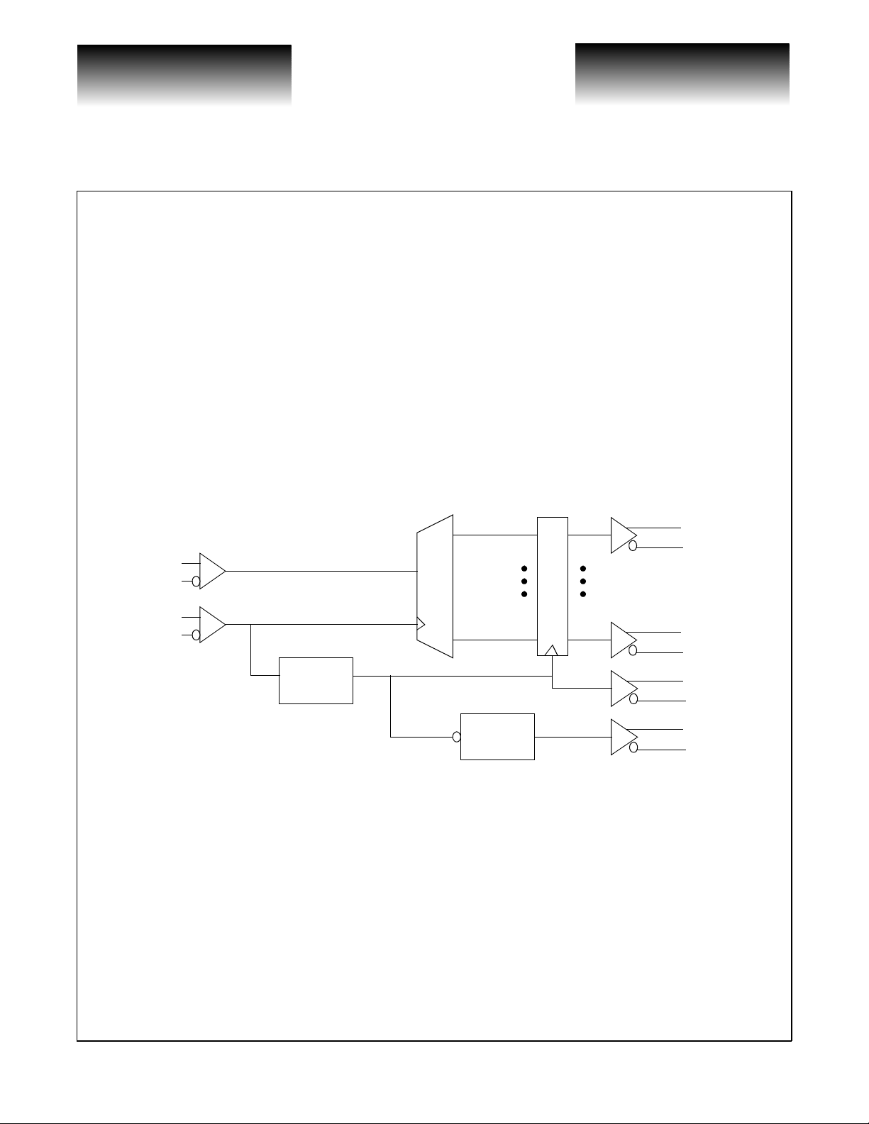
VSC8164 Block DIagram
Output Register
DI+
DI-
D0+
D0-
HSCLKI+
HSCLKI-
Divide by
16
Divide by
2
D15+
D15-
CLK16O+
CLK16O-
CLK32O+
CLK32O-
Functional Description
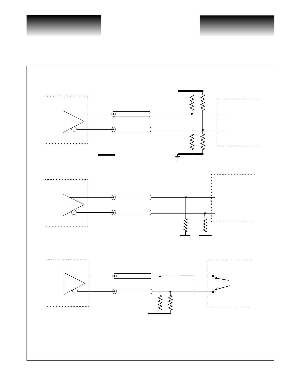
Low Speed Interface
The demultiplexed serial stream is made available by a 16 bit differential LVPEC L interface D[15:0] with
accompanying differential LVPECL divide by 16 clock CLK16O
speed LVPECL output drivers are designed to drive a 50
terminated with a spli t end terminat ion scheme (see Figur e 1), or DC ter minate d b y 50
(see Figure 2). At any time, the equivalent split-end termination technique can be substituted for the traditional
50
Ω to V
coupling method for the occasion when the downstream device provides the bias point for AC coupling. If the
downstream device were to have internal termination, the line to line 100
divide by 32 output can be used to provide a reference clock for the clock multiplication unit on the VSC8163.
-2V on each line. AC coupling can be a chi eved by a number of methods. Figure 3 illustrat es an AC
CC
Ω transmission line. The transmission line can be DC
± and divide by 32 clock CLK32O±. The low
Ω to V
Ω resistor may not be necessary. The
-2V on each line
CC
G52239-0, Rev. 3.3 VITESSE SEMICONDUCTOR CORPORATION Page 1
5/17/00 741 Calle Plano, Camarillo, CA 93012 • 805/388-3700 • FAX: 805/987-5896
Page 2
VITESSE
SEMICONDUCTOR CORPORATION
2.488 Gbit/sec to 2.7Gbit/sec
Preliminary Datasheet
1:16 SONET/SDH Demux
Figure 1: Split-end DC Termination of Low Speed LVPECL CLK16O, CLK32O, D[15:0] Outputs
VCC
VSC8164
R1||R2 = Zo , R1 = 125Ω R2 = 83Ω
VCCR2 + VEER1
R1+R2
Figure 2: Traditional DC Termination of Low Speed LVPECL CLK16O, CLK32O, D[15:0] Outputs
= V
Z
Z
o
o
Term
VEE
R1
R2
R1
downstream
R2
downstream
VSC8164
Z
o
VSC8164
R1 =50Ω
VCC-2V
Figure 3: AC Termination of Low Speed LVPECL CLK16O, CLK32O, D[15:0] Outputs
VSC8164
Z
o
Z
o
50Ω
50Ω
V
CC
100nF
100nF
-2V
R1 =50
Ω
VCC-2V
downstream
bias point
generated
internally
Page 2 VITESSE SEMICONDUCTOR CORPORATION G52239-0, Rev. 3.3
741 Calle Plano, Camarillo, CA 93012 • 805/38 8-37 00 • FAX: 805/987- 589 6 5/17/00
Page 3
VITESSE
SEMICONDUCTOR CORPORATION
reliminary Datasheet
SC8164
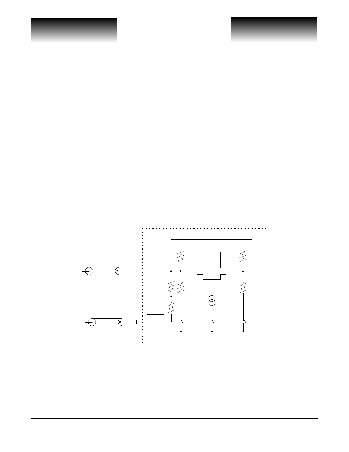
High Speed Interface
2.488 Gbit/sec to 2.7Gbit/sec
1:16 SONET/SDH Demux
The incoming 2.488Gb/s data (up to 2.7Gb/s for FEC applications) and input clock are received by high
speed inputs DI and HSC LKI. The da ta and clock inputs are in ternally te rminated by a ce nter-tapped resi stor
network. For differential input DC coupling, the network is terminated to the appropriate termination voltage
V
(pins HSDREF, HSCLKREF) providing a 50Ω to V
Term
For differential input AC coupling, the network is terminated to
termination for both true and complement inputs.
Term
V
via a blocking capacitor.
Term
In most situations these inputs will have high transition density and little DC offset. However, in cases
where this does not hold, direct DC connection is possible. All serial dat a and clock inputs ha ve the same circuit
topology, as shown in Figure 4. The reference voltage is created by a resistor divider as shown. If the input signal is driven differentially and DC-coupled to the part, the mid-point of the input signal sw ing should be centered about this reference voltage and not exceed the maximum allowable amplitude (
∆V
CMI
, ∆V
IHSDC
single-ended, DC-coupling operations, it is recommended that the user provides an external reference voltage
which has better temperature and power supply nois e rejection than the on-chip r esistor divider. The external
reference should have a nominal value equivalent to the common mode switch point of the DC coupled signal,
and can be connected to either side of the differential gate.
Figure 4: High Speed Serial Clock and Data Inputs
Chip Boundary
). For
VCC = 3.3V
Z
Supplies
C
TYP = 100 nF
IN
TYP = 100 nF
C
AC
O
V
Term
Z
O
C
IN
C
AC
C
IN
50Ω
50Ω
= 0V
V
EE
This device is specified as a LVPECL device with a single positive 3.3V supply. Should the user desire to
use the device in a ECL environment with a negative 3.3V supply, t hen VCC will be ground and VEE w ill be -
3.3V.
G52239-0, Rev. 3.3 VITESSE SEMICONDUCTOR CORPORATION Page 3
5/17/00 741 Calle Plano, Camarillo, CA 93012 • 805/388-3700 • FAX: 805/987-5896
Page 4
VITESSE
SEMICONDUCTOR CORPORATION
2.488 Gbit/sec to 2.7Gbit/sec
1:16 SONET/SDH Demux
Decoupling of the power supplies is a critical element in maintaining the proper operation of the part. It is
recommended that the V
on each V
also be placed in parallel with the 0.1
low inductance ceramic SMT X7R devices. For the 0.1
0.01
µF and 0.001µF capacitors can be either 0603 or 0402 packages.
For low frequency decoupling, 47
board’s main +3.3V power supply and placed close to the C-L-C pi filter.
If the device is being used in an ECL environment with a -3.3V supply, then all references to decoupling
V
must be changed to VEE, and all references to decoupling 3.3V must be changed to -3.3V.
CC
power supply pin as close to the package as possible. If room permits, a 0.001µF capacitor should
CC
power supply be decoupled using a 0.1µF and 0.01µF capacit or placed in parallel
CC
µF and 0.01µF capacitors mentioned above. Recommended capacitors are
µF capacitor, a 0603 package should be used. The
µF tantalum low inductance SMT caps should be sprinkled over the
AC Characteristics
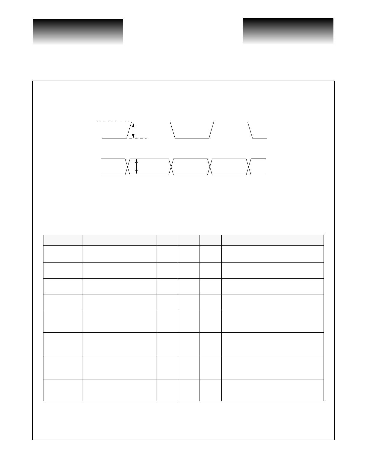
Figure 5: AC Timing Waveforms
CLK16O+
Parallel data clock output
t
Preliminary Datasheet
VSC8164
pdd
D(0...15)+
Parallel data outputs
CLK32O+
Parallel data clock output
DI+
High speed differential serial data input
HSCLKI+
High speed differential clock input
VALID DATA (1) VALID DATA (2)
t
pd32
Figure 6: High Speed Input Timing
D0
D1 D2
D4 D5 D6 D7 D8 D9 D10 D11 D12
D3
t
dsu
D13D14 D15
t
dh
Page 4 VITESSE SEMICONDUCTOR CORPORATION G52239-0, Rev. 3.3
741 Calle Plano, Camarillo, CA 93012 • 805/38 8-37 00 • FAX: 805/987- 589 6 5/17/00
Page 5
VITESSE
SEMICONDUCTOR CORPORATION
reliminary Datasheet
SC8164
Figure 7: Differential and Single Ended Input and Output Voltage Measurement
2.488 Gbit/sec to 2.7Gbit/sec
1:16 SONET/SDH Demux
b
Single
= α
Ended
a
b
Swing
Differential
Swing
= α
a
* Differential swing (α) is specified as | b - a | ( or | a - b | ), as is the single ended swing.
Differential swing is specified as equal in magnitude to single ended swing.
Table 1: AC Characteristics
Parameters Description Min Max Units Conditions
t
pdd
t
pd32
tDR, t
t
, t
CLKR
CLK16O
t
dsu
t
dh
HSCLKI
DF
CLKF
D
D
Data valid from falling
edge of CLK16O+
CLK32O transition from
falling edge of CLK16O+
D[15:0]+/- rise and fall
times
CLK16O+/- rise and fall
times
CLK16O+/- duty cycle
distortion
DI+ setup time with respect
to falling edge of
HSCLKI+
DI+ hold time with respect
to falling edge of
HSCLKI+
HSCLKI+/- duty cycle
distortion
0800ps.
01.0ns.
—
—
45 55
100 — ps
75 — ps
40 60
400 ps
250 ps
% of
clock
cycle
% of
clock
cycle
20% to 80% into 50 Ohm load.
See Figure 7
20% to 80% into 50 Ohm load.
See Figure 7
High speed clock input at 2.488GHz
G52239-0, Rev. 3.3 VITESSE SEMICONDUCTOR CORPORATION Page 5
5/17/00 741 Calle Plano, Camarillo, CA 93012 • 805/388-3700 • FAX: 805/987-5896
Page 6

VITESSE
SEMICONDUCTOR CORPORATION
2.488 Gbit/sec to 2.7Gbit/sec
Preliminary Datasheet
1:16 SONET/SDH Demux
Table 2: DC Characteristics (Over recommended operating conditions).
Parameters Description Min Typ Max Units Conditions
V
V
∆V
OLVPECL
∆V
∆V
∆V
V
OH
OL
IHSAC
IHSDC
CMI
CC
P
D
I
DD
PECL output high
voltage
PECL output low
voltage
Low speed output
voltage differential peakto-peak swing.
Serial input differential
voltage AC coupled
Serial input differential
voltage DC coupled
Serial input common
mode voltage
Supply volta ge
Power dissipation
Supply Current
VCC-1.02 — VCC-0.70 V
VCC-
2.00
400 — 1300 mV
200 ——mV
200 ——mV
VCC-1.5 VCC-0.5 V
3.14 — 3.47 V
—
—
— V
.75 1.1 W
220 320 mA
-1.62 V
CC
50Ω Termination to VCC -
2.0V, See Figure 7
50Ω Termination to VCC -
2.0V, See Figure 7
AC Coupled
AC Coupled, internally
biased to (V
DC coupled
3.3V± 5%
Outputs open,
V
= 3.45V
CC
Outputs open,
V
= 3.45V
CC
VSC8164
CC+VEE
)/2
Figure 8: Parametric Measurement Information
PECL Rise and Fall Time
80%
20%
T
r
Page 6 VITESSE SEMICONDUCTOR CORPORATION G52239-0, Rev. 3.3
741 Calle Plano, Camarillo, CA 93012 • 805/38 8-37 00 • FAX: 805/987- 589 6 5/17/00
T
f
Parametric Test Load Circuit
PECL Output Load
Z0 = 50Ω
50Ω
VCC-2.0V
Page 7

VITESSE
SEMICONDUCTOR CORPORATION
reliminary Datasheet
SC8164
Absolute Maximum Ratings
Power Supply Voltage, (VCC).......................................................................................................-0.5V to +3.8V
DC Input Voltage (Differential inputs)..................................................................................-0.5V to V
Output Current (Differential Outputs)....................................................................................................+/-50mA
Case Temperature Under Bias......................................................................................................-55
Storage Temperature..................................................................................................................-65
Maximum Input ESD (Human Body Model).............................................................................................1500V
(1)
2.488 Gbit/sec to 2.7Gbit/sec
1:16 SONET/SDH Demux
+0.5V
cc
o
to +125oC
o
C to +150oC
Recommended Operating Conditions
Power Supply Voltage, (VCC)..............................................................................................................+3.3V+5%
o
Operating Temperature Range .........................................................0
Notes:
(1) CAUTION: Stresses listed under “Absolute Maximum Ratings” may be applied to devices one at a time without causing per-
manent damage. Functionality at or above the values listed is not implied. Exposure to these values for extended periods
may affect device reliability.
C Ambient to +85oC Case Temperature
ESD Ratings
Proper ESD procedures should be used wh en handl ing t his produ ct. Th e VSC8164 is rate d to t he foll o wing ESD
voltages based on the human body model:
1. All pins are rated at or above 1500V.
G52239-0, Rev. 3.3 VITESSE SEMICONDUCTOR CORPORATION Page 7
5/17/00 741 Calle Plano, Camarillo, CA 93012 • 805/388-3700 • FAX: 805/987-5896
Page 8

VITESSE
SEMICONDUCTOR CORPORATION
2.488 Gbit/sec to 2.7Gbit/sec
1:16 SONET/SDH Demux
Package Pin Descriptions
Table 3: Pin Identification
Pin Name I/O Level Description
1
2
3
4
5
6
7
8
9
10
11
12
13
14
15
16
17
18
19
20
21
22
23
24
25
26
27
28
29
30
31
32
33
NC - - No connect, leave unconnected
NC - - No connect, leave unconnected
NC
NC - - No connect, leave unconnected
NC - - No connect, leave unconnected
NC - - No connect, leave unconnected
NC - - No connect, leave unconnected
NC - - No connect, leave unconnected
NC - - No connect, leave unconnected
HSDREF I voltage High speed data input termination voltage reference
NC - - No connect, leave unconnected
VEE
D+ I HS High jspeed data input, true
D- I HS High speed data input, complement
VCC - +3.3V typ Positive power supply pins
VEE
VEE
VCC - +3.3V typ Positive power supply pins
HSCLK- I HS High speed clock input, complement
HSCLK+ I HS High speed clock inp u t , tr ue
VCC - +3.3V typ Positive power supply pins
HSCLKREF I voltage High speed clock input termination voltage reference
NC - - No connect, leave unconnected
NC - - No connect, leave unconnected
NC - - No connect, leave unconnected
NC - - No connect, leave unconnected
NC - - No connect, leave unconnected
NC - - No connect, leave unconnected
NC - - No connect, leave unconnected
NC - - No connect, leave unconnected
NC - - No connect, leave unconnected
NC - - No connect, leave unconnected
NC - - No connect, leave unconnected
Preliminary Datasheet
VSC8164
- - No connect, leave unconnected
- GND typ Negative power supply pins
- GND typ Negative power supply pins
- GND typ Negative power supply pins
Page 8 VITESSE SEMICONDUCTOR CORPORATION G52239-0, Rev. 3.3
741 Calle Plano, Camarillo, CA 93012 • 805/38 8-37 00 • FAX: 805/987- 589 6 5/17/00
Page 9

VITESSE
SEMICONDUCTOR CORPORATION
reliminary Datasheet
SC8164
Pin Name I/O Level Description
34
35
36
37
38
39
40
41
42
43
44
45
46
47
48
49
50
51
52
53
54
55
56
57
58
59
60
61
62
63
64
65
66
67
68
69
NC - - No connect, leave unconnected
NC - - No connect, leave unconnected
NC - - No connect, leave unconnected
NC - - No connect, leave unconnected
NC - - No connect, leave unconnected
NC - - No connect, leave unconnected
NC - - No connect, leave unconnected
NC - - No connect, leave unconnected
NC - - No connect, leave unconnected
NC - - No connect, leave unconnected
NC - - No connect, leave unconnected
NC - - No connect, leave unconnected
NC - - No connect, leave unconnected
NC - - No connect, leave unconnected
NC - - No connect, leave unconnected
NC - - No connect, leave unconnected
NC - - No connect, leave unconnected
NC - - No connect, leave unconnected
NC - - No connect, leave unconnected
NC - - No connect, leave unconnected
VCC - +3.3V typ Positive power supply pins
NC - - No connect, leave unconnected
NC - - No connect, leave unconnected
VEE
D15+ O LVPECL Low spee d differential parallel data
D15- O LVPECL Low speed differential parallel data
VCC - +3.3V typ Positive power supply pins
D14+ O LVPECL Low spee d differential parallel data
D14- O LVPECL Low speed differential parallel data
NC - - No connect, leave unconnected
VCC - +3.3V typ Positive power supply pins
NC - - No connect, leave unconnected
VCC - +3.3V typ Positive power supply pins
D13+ O LVPECL Low spee d differential parallel data
D13- O LVPECL Low speed differential parallel data
VEE
2.488 Gbit/sec to 2.7Gbit/sec
1:16 SONET/SDH Demux
- GND typ Negative power supply pins
- GND typ Negative power supply pins
G52239-0, Rev. 3.3 VITESSE SEMICONDUCTOR CORPORATION Page 9
5/17/00 741 Calle Plano, Camarillo, CA 93012 • 805/388-3700 • FAX: 805/987-5896
Page 10

VITESSE
SEMICONDUCTOR CORPORATION
2.488 Gbit/sec to 2.7Gbit/sec
1:16 SONET/SDH Demux
Pin Name I/O Level Description
70
71
72
73
74
75
76
77
78
79
80
81
82
83
84
85
86
87
88
89
90
91
92
93
94
95
96
97
98
99
100
101
102
103
104
105
D12+ O LVPECL Low spee d differential parallel data
D12- O LVPECL Low speed differential parallel data
VCC - +3.3V typ Positive power supply pins
D11+ O LVPECL Low spee d differential parallel data
D11- O LVPECL Low speed differential parallel data
VCC - +3.3V typ Positive power supply pins
D10+ O LVPECL Low spee d differential parallel data
D10- O LVPECL Low speed differential parallel data
VEE
D9+ O LVPECL Low speed differential parallel data
D9- O LVPECL Low speed differential parallel data
VCC - +3.3V typ Positive power supply pins
D8+ O LVPECL Low speed differential parallel data
D8- O LVPECL Low speed differential parallel data
VCC - +3.3V typ Positive power supply pins
D7+ O LVPECL Low speed differential parallel data
D7- O LVPECL Low speed differential parallel data
VEE
D6+ O LVPECL Low speed differential parallel data
D6- O LVPECL Low speed differential parallel data
VCC - +3.3V typ Positive power supply pins
D5+ O LVPECL Low speed differential parallel data
D5- O LVPECL Low speed differential parallel data
VCC - +3.3V typ Positive power supply pins
D4+ O LVPECL Low speed differential parallel data
D4- O LVPECL Low speed differential parallel data
VEE
D3+ O LVPECL Low speed differential parallel data
D3- O LVPECL Low speed differential parallel data
VCC - +3.3V typ Positive power supply pins
D2+ O LVPECL Low speed differential parallel data
D2- O LVPECL Low speed differential parallel data
VCC - +3.3V typ Positive power supply pins
VCC - +3.3V typ Positive power supply pins
NC - - No connect, leave unconnected
D1+ O LVPECL Low speed differential parallel data
Preliminary Datasheet
VSC8164
- GND typ Negative power supply pins
- GND typ Negative power supply pins
- GND typ Negative power supply pins
Page 10 VITESSE SEMICONDUCTOR CORPORATION G52239-0, Rev. 3.3
741 Calle Plano, Camarillo, CA 93012 • 805/38 8-37 00 • FAX: 805/987- 589 6 5/17/00
Page 11

VITESSE
SEMICONDUCTOR CORPORATION
reliminary Datasheet
SC8164
Pin Name I/O Level Description
106
107
108
109
110
111
112
113
114
115
116
117
118
119
120
121
122
123
124
125
126
127
128
D1- O LVPECL Low speed differential parallel data
VCC - +3.3V typ Positive power supply pins
D0+ O LVPECL Low speed differential parallel data
D0- O LVPECL Low speed differential parallel data
VEE
CLK16O- O LVPECL Parallel clock output, complement
CLK16O+ O LVPECL Parallel clock output, true
VCC - +3.3V typ Positive power supply pins
CLK32O- O LVPECL Divided parallel clock output, compl e ment
CLK32O+ O LVPECL Divided parallel clock output, true
NC - - No connect, leave unconnected
NC - - No connect, leave unconnected
NC - - No connect, leave unconnected
NC - - No connect, leave unconnected
NC - - No connect, leave unconnected
NC - - No connect, leave unconnected
NC - - No connect, leave unconnected
NC - - No connect, leave unconnected
NC - - No connect, leave unconnected
NC - - No connect, leave unconnected
NC - - No connect, leave unconnected
NC - - No connect, leave unconnected
NC - - No connect, leave unconnected
2.488 Gbit/sec to 2.7Gbit/sec
1:16 SONET/SDH Demux
- GND typ Negative power supply pins
Note: No connect (NC) pins must be left unconnected, or floating. Connecting any of these pins to either the positive or nega-
tive power supply rails may cause improper operation or failure of the device; or in extreme cases, cause permanent
damage to the device.
G52239-0, Rev. 3.3 VITESSE SEMICONDUCTOR CORPORATION Page 11
5/17/00 741 Calle Plano, Camarillo, CA 93012 • 805/388-3700 • FAX: 805/987-5896
Page 12

VITESSE
SEMICONDUCTOR CORPORATION
2.488 Gbit/sec to 2.7Gbit/sec
1:16 SONET/SDH Demux
Package Information
PIN 128
PIN 1
RAD. 2.92 ± .50
EXPOSED
INTRUSION
0.127 MAX.
EXPOSED
HEATSINK
PIN 38
10° TYP .
(2)
2.54 ± .50
D
1
D
TOP VIEW
128 PQFP Package Drawings
PIN 102
E
E
1
PIN 64
Preliminary Datasheet
VSC8164
Key mm Tolerance
A2.35 MAX
A1 0.25 MAX
A2 2.00 +.10
D 17.20 ±.20
D1 14.00 ±.10
E 23.20 ±.20
E1 20.00 ±.10
L .88 +.15/-.10
e.50BASIC
b .22 ±.05
θ 0°-7°
R.30 TYP
R1 .20 TYP
A
2
Notes: 1) Drawing is not to scale
2) All dimensions in mm
3) Package represented is
also used for the 64,
80, & 100 PQFP packages.
Pin count drawn does
not reflect the 128 Package.
A
1
10° TYP .
R
R1
θ
1
.25
A
θ
MAX.
0.17
L
e
b
A
STANDOFF
A
1
LEAD COPLANARITY
NOTES:
Package #: 101-322-5
Issue #: 2
Page 12 VITESSE SEMICONDUCTOR CORPORATION G52239-0, Rev. 3.3
741 Calle Plano, Camarillo, CA 93012 • 805/38 8-37 00 • FAX: 805/987- 589 6 5/17/00
Page 13

VITESSE
SEMICONDUCTOR CORPORATION
2.488 Gbit/sec to 2.7Gbit/sec
1:16 SONET/SDH Demux
Preliminary Datasheet
VSC8164
Package Thermal Considerations
This package has been enhanced with a copper heat slug to provide a low thermal resistance path from the
die to the exposed surface of the heat spreader. The thermal resistance is shown in the following table
Table 4: Thermal Resistance
Symbol Description °C/W
θ
jc
θ
ca
Thermal Resistance with Airflow
Shown in the table below is the thermal resistance with airflo w. This thermal resistance value reflects all the
thermal paths including through the leads in an environment where the leads are exposed. The temperature difference between the amb ient airfl ow temperature and the ca se temperatur e should be the wors t case power of
the device multiplied by the thermal resistance.
Thermal resistance from
junction to case.
Thermal resistance from case to
ambient with no airflow,
including condu ction through
the leads.
1.34
25.0
Table 5: Thermal Resistance with Airflow
Airflow θca (
100 lfpm 21
200 lfpm 18
400 lfpm 16
600 lfpm 14.5
Maximum Ambient Temperature without Heatsink
The worst case ambient temperature without use of a heatsink is given by the equation:
where:
θ
Theta case to ambient at appropriate airflow
CA
Τ
A(MAX)
Τ
C(MAX
P
(MAX)
Ambient Air temperature
Case temperature (85oC for VSC8164)
)
Power (1.1 W for VSC8164)
o
C/W)
T
AMAX()TCMAX()
=
P–
MAX()
θ
CA
Page 13 VITESSE SEMICONDUCTOR CORPORATION G52239-0, Rev. 3.3
741 Calle Plano, Camarillo, CA 93012 • 805/38 8-37 00 • FAX: 805/987- 589 6 5/17/00
Page 14

VITESSE
SEMICONDUCTOR CORPORATION
2.488 Gbit/sec to 2.7Gbit/sec
1:16 SONET/SDH Demux
The results of this calculation are listed below:
Table 6: Maximum Ambient Air Temperature without Heatsink
Airflow
none 58
100 lfpm 62
200 lfpm 65
400 lfpm 67
600 lfpm 69
Note that ambient air temperature varies throughout the system based on the positioning and magnitude of
heat sources and the direction of air flow.
Max Ambient Temp oC
Preliminary Datasheet
VSC8164
Page 14 VITESSE SEMICONDUCTOR CORPORATION G52239-0, Rev. 3.3
741 Calle Plano, Camarillo, CA 93012 • 805/38 8-37 00 • FAX: 805/987- 589 6 5/17/00
Page 15

VITESSE
SEMICONDUCTOR CORPORATION
2.488 Gbit/sec to 2.7Gbit/sec
1:16 SONET/SDH Demux
Preliminary Datasheet
VSC8164
Ordering Information
The order number for this product is formed by a combination of the device number, and package type.
VSC8164
Device Type
VSC8164:
2.488Gb/s to 2.7Gb/s
1:16 SONET/SDH Demux
QR
Package
QR: 128PQFP, 14X20mm Body
Notice
This document contains information about a new product in the preproduction phase of development. The
information contained in this document is based on initial product characterization. Vitesse reserves the right to
alter specifications, features, capabilities, functions, manufacturing release dates, and even general availability
of the product at any time. The reader is cautioned to confirm that this datasheet is current prior to using it for
design.
Warning
Vitesse Semiconductor Corporation’s product are not intended for use in life support appliances, devices or
systems. Use of a Vitesse product in such applications without written consent is prohibited.
Page 15 VITESSE SEMICONDUCTOR CORPORATION G52239-0, Rev. 3.3
741 Calle Plano, Camarillo, CA 93012 • 805/38 8-37 00 • FAX: 805/987- 589 6 5/17/00
Page 16

VITESSE
SEMICONDUCTOR CORPORATION
2.488 Gbit/sec to 2.7Gbit/sec
1:16 SONET/SDH Demux
Preliminary Datasheet
VSC8164
Page 16 VITESSE SEMICONDUCTOR CORPORATION G52239-0, Rev. 3.3
741 Calle Plano, Camarillo, CA 93012 • 805/38 8-37 00 • FAX: 805/987- 589 6 5/17/00
 Loading...