

Page 1
VITESSE
SEMICONDUCTOR CORPORATION
Page 1
8/28/98 741 Calle Plano, Camarillo, CA 93012 • 805/388-3700 • FAX: 805/987-5896
VITESSE
SEMICONDUCTOR CORPORATION
Advance Product Information
SC8161
2.488Gb/s SONET / SDH
16:1 Mux with Clock Generator and Laser Driver
G52208-0, Rev.2.1
Features
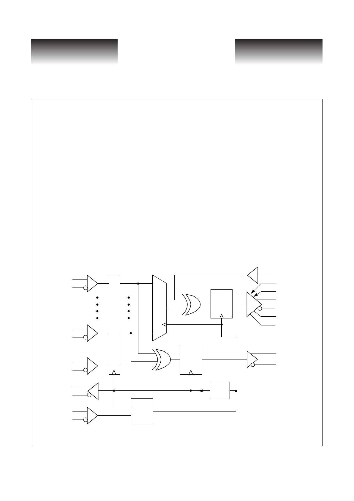
General Description
The VSC8161 combines a Laser Driver and a clock multiplier with a 16:1 multiplexer to provide a singlechip solution. The 16-bit data word is latched by an internal version of the reference clock, and is bit-multiplexed up to 2.488GHz. The on-chip PLL generates the internal 2.488GHz clock, which remains locked to the
155.52 MHz reference clock. The on-chip laser driver pro vides up to 60 mA modulation current and 50 mA bias
current.
VSC8161 Functional Block Diagram
• 16:1 Multiplexer Integrated with Clock
Multiplier and Laser Driver
• Monolithic Phase Locked Loop
• Laser Driver Provides up to 110 mA Current
• Differential 16-bit Parallel Data
• 100 pin 14x14 Plastic Quad Flat Package
• Jitter Generation Meets SONET OC-48 and
SDH STM-16 Requirements
• Companion to the VSC8162 1:16 Demultiplexer with Clock Recovery
• Supports Parity Checking at the 16-bit
Parallel Interface
D0+
D0-
D15+
D15-
PARITY+
PARITY-
CLK16+
CLK16-
REFCK+
REFCK-
DINVERT
VIP
VIB
IOUT+
IOUT-
MIP
MIB
DINVALID+
DINVALID-
Output
Retime
Parity
Register
2.5GHz
PLL
Divide
by 16
Input Register
Page 2
Page 2
VITESSE
SEMICONDUCTOR CORPORATION
741 Calle Plano, Camarillo, CA 93012 • 805/388-3700 • FAX: 805/987-5896 8/28/98
VITESSE
SEMICONDUCTOR CORPORATION
Advance Product Information
VSC8161
.488Gb/s SONET / SDH
16:1 Mux with Clock Generator and Laser Driver
G52208-0, Rev.2.1
Functional Description
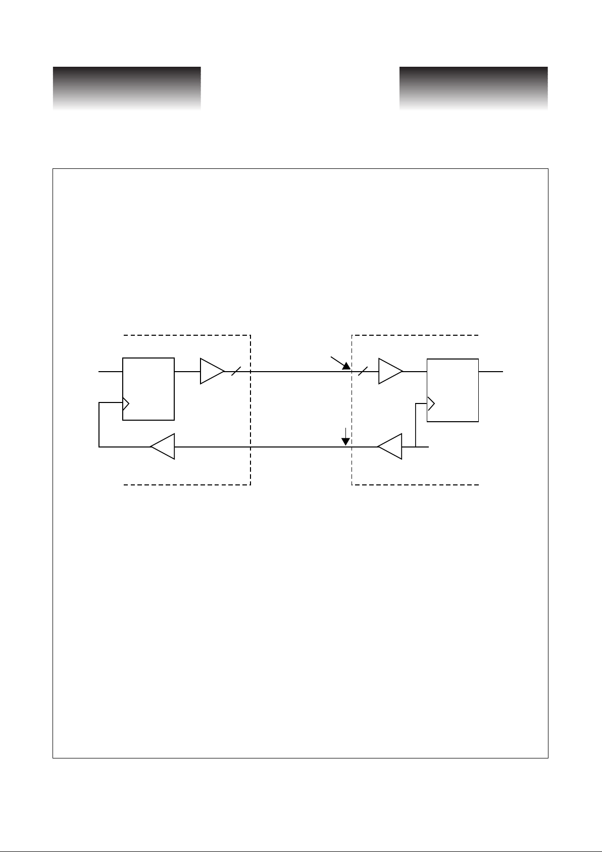
Multiplexer
The VSC8161 takes incoming 16-bit wide data at 155 MHz, D0 through D15, and converts it into a serial
data stream, with D0 transmitted first. CLK16 is the 155MHz low-speed clock output which is created by dividing the internally generated 2.488 GHz clock by 16. The upstream device should use the CLK16 as its internal
reference and to register its low-speed data and parity output signals (See Fig 1). Care needs to be taken to meet
the data setup and hold timing on the parallel data.
Figure 1: VSC8161 Parallel Data Interface
The timing relationship between the VSC8161 and the upstream device is described by the waveforms in
Fig. 5 and the associated parameters: t
D
, t
DSU
, and t
DH
appearing in Table 1.
The polarity of the serialized data can be inverted by the assertion of the DINVERT input. In either case,
however, the signal is retimed prior to the Laser Driver section of the VSC8161.
Clock Multiplier
The clock multiplier is fully integrated. No external components are needed. Jitter Generation of the clock
multiplier meets the requirement of Bellcore’s GR-253 (SONET) document. As in all of the frequency synthesizers that employ a PLL, it is important to choose REFCK to be as
jitter-free as possible.
In Out
CK
In Out
CK
"upstream device"
D [0:15]
VSC8161
CLK16
16
16
Page 3
VITESSE
SEMICONDUCTOR CORPORATION
Page 3
8/28/98 741 Calle Plano, Camarillo, CA 93012 • 805/388-3700 • FAX: 805/987-5896
VITESSE
SEMICONDUCTOR CORPORATION
Advance Product Information
SC8161
2.488Gb/s SONET / SDH
16:1 Mux with Clock Generator and Laser Driver
G52208-0, Rev.2.1
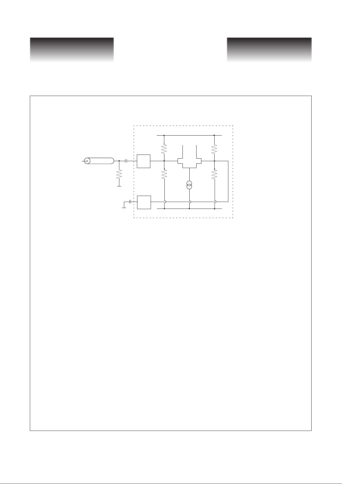
Figure 2: Single-ended AC-Coupling for REFCK+, REFCK– Inputs
A differential input buffer is used to supply the reference clock to the clock multiplier. Internal biasing will
position the reference voltage of approximately -1.32V on both the true and complement inputs. This input can
either be DC-coupled or AC-coupled; it can also be driven single-ended or differentially. Figure 2 shows the
configuration for single-ended, AC-coupled operation. In the case of direct coupled and single-ended input, it is
recommended that a stable V
REF
for ECL levels be used for the complementary input if the input common mode
voltage is not -1.32V.
Parity
Systems employing internal parity are supported by the VSC8161. A parity check is performed between the
PARITY input and the 16 data bits. Even parity is expected. In other words, the DINVALID output is the XOR
of all 16 parallel data bits and the PARITY input. If the Exclusive-OR gate fails to confirm even parity, the DINVALID output will be asserted. DINVALID becomes available t
DV
after the falling edge of CLK16. DINVALID
is a NRZ pulse that is updated every 6.4 ns, i.e., the period of CLK16. The timing relationship of DINVALID to
CLK16 is shown in Figure 6.
The DINVALID pins may be left open if parity is unused.
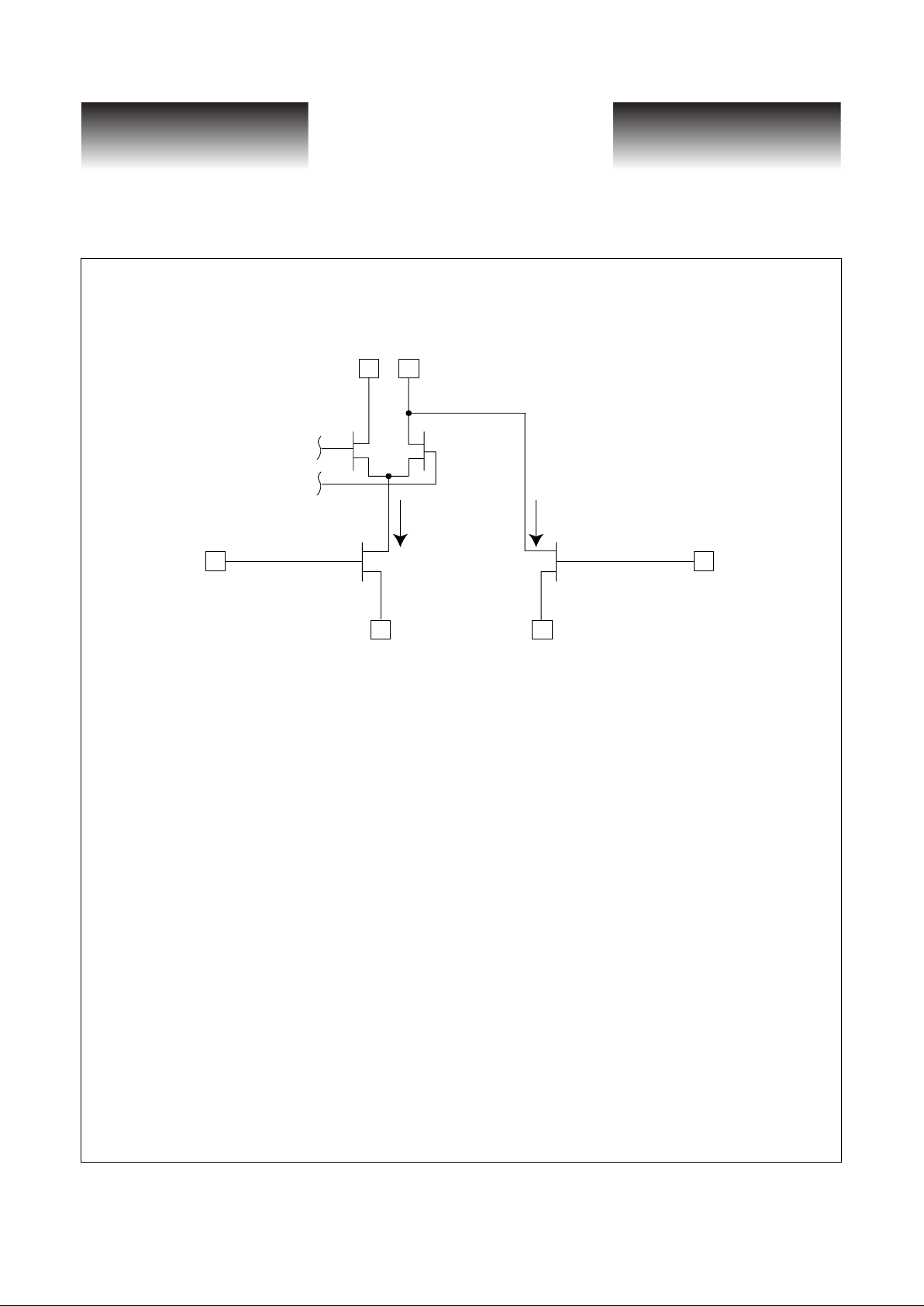
Laser Driver
The laser driver contained in the VSC8161 provides up to 50mA of DC bias current and 60 mA of modulation current. Direct control of the laser bias and modulation current is provided. Laser bias and modulation current levels are monitored and controlled using external components.
A schematic representation of the laser driver output stage showing the relationship between the the external controls signals and the internal circuitry is provided in Figure 3.
V
TT
REFCK-
V
CC
= GND
V
TT
= -2V
-1.32V
-1.32V
R
| |
= 1kΩ (Min.)
C
IN
C
SE
V
TT
Chip Boundary
CIN TYP = 0.1µF
C
SE
TYP = 0.1µF for single ended applications. (Capacitor values are
Z
O
RT = Z
O
selected for REFCK = 155.52 MHz)
REFCK+
Page 4
Page 4
VITESSE
SEMICONDUCTOR CORPORATION
741 Calle Plano, Camarillo, CA 93012 • 805/388-3700 • FAX: 805/987-5896 8/28/98
VITESSE
SEMICONDUCTOR CORPORATION
Advance Product Information
VSC8161
.488Gb/s SONET / SDH
16:1 Mux with Clock Generator and Laser Driver
G52208-0, Rev.2.1
Figure 3: Laser Driver Output
IOUT+, IOUT- Outputs
The IOUT+ and IOUT- pins are designed to interface to a laser diode. A logic “0” appears as less current
(higher voltage) at the IOUT+ pin, and less light from a series laser diode. A logic “1” appears as more current
(lower voltage) at the IOUT+ pin, and more light from a series laser diode. The polarity can be reversed through
use of the DINVERT signal pin. The current difference depends upon the voltage (VIP - MIP) applied at the
VIP pin. Applying (VIP - MIP) = 0V will turn off the modulation current. Applying (VIP - MIP) = approximately 2V will maximize the modulation current. Applying (VIP - MIP) up to 5.2V is allowed, but not likely to
be useful. Use caution to avoid exceeding the absolute maximum current ratings (see table). Operation of the
bias current is independent of, and similar to, the operation of the modulation current. Pins MIB and VIB are
used to monitor and control the bias current.
It is recommended that feed back circuits be utilized to regulate the desired modulation and bias currents.
This is illustrated with examples in figure 4. Separate circuits are used, since the modulation and bias currents
are independent.
X X
IOUT– IOUT+
OUTPUT
DIFF
PAIR
X
MIB
X
VIP
X
MIP
I
MOD
I
BIAS
X
VIB
Page 5
VITESSE
SEMICONDUCTOR CORPORATION
Page 5
8/28/98 741 Calle Plano, Camarillo, CA 93012 • 805/388-3700 • FAX: 805/987-5896
VITESSE
SEMICONDUCTOR CORPORATION
Advance Product Information
SC8161
2.488Gb/s SONET / SDH
16:1 Mux with Clock Generator and Laser Driver
G52208-0, Rev.2.1
Figure 4: Recommended Modulation and Bias Current Control Circuits
Supplies
The VSC8161 is designed to operate with V
EE
= -5.2V, V
TT
= -2.0V and V
CC
= GND (0.0V). However, the
part can be operated in an all positive supply en vironment, or a mix ed positi ve and ne gati v e supply en vironment.
To operate in an all positive supply environment, each of the supply voltages must be shifted up by 5.2V
such that V
EE
will now be GND, V
TT
= +3.2V and V
CC
= +5.2V. To operate in a mixed positive and negative
supply environment, each of the supply voltages must be shifted up by 2.0V such that V
TT
will now be GND,
V
EE
= -3.2V and V
CC
= +2.0V
.
Bear in mind that termination voltages must be adjusted to reflect any shift in supply voltages.
X
VIP
X
MIP
–
+
1Ω
–
+
V
EE
V
P
(0-60mV)
X
VIB
X
MIB
–
+
1Ω
–
+
V
EE
V
B
(0-50mV)
Bias Current Control Circuit
Modulation Current Control Circuit
For Example to get 40mA of modulation current, VP is set to 40mV (40mA x 1Ω = 40mV)
Page 6

Page 6
VITESSE
SEMICONDUCTOR CORPORATION
741 Calle Plano, Camarillo, CA 93012 • 805/388-3700 • FAX: 805/987-5896 8/28/98
VITESSE
SEMICONDUCTOR CORPORATION
Advance Product Information
VSC8161
.488Gb/s SONET / SDH
16:1 Mux with Clock Generator and Laser Driver
G52208-0, Rev.2.1
VSC8161 Electrical Characteristics
Table 1: Multiplexer AC Characteristics
(
Over recommended operating range
)
Figure 5: VSC8161 Parallel Interface AC Characteristics
Figure 6: VSC8161 Parity Interface
Parameter
Description Min Typ Max Units
t
D
CLK16 period - 6.4 - ns
t
DSU
Parallel data set-up time (wrt CLK16 falling edge) 1.7 - - ns
t
DH
Data hold time (wrt CLK16 falling edge) 0.3 - - ns
t
DC
CLK16 duty cycle 45 - 55 %
t
r
, t
f
REFCK+/- rise and fall times (10%-90%) - - 1.5 ns
t
r
, t
f
D(0..15)+/- rise and fall times (10%-90%) - - 2.0 ns
t
r
, t
f
CLK16+/- rise and fall times (10%-90%) - 0.7 1 ns
t
DINV
Duration of Data Invalid Pulse - 6.4 - ns
t
DV
Parallel Data to DINVALID -
3t
D
+
0.3ns
-ns
VALID DATA (1)
VALID DATA (2)
D0 D1 D2 D3 D4 D5 D6 D7 D8 D9 D10 D11 D12 D13 D14 D15
Parallel data clock output
Parallel data inputs
High speed differential serial data output
CLK16+
D(0...15),PARITY
IOUT+/-
Serialized Data
t
D
t
D
t
DH
t
DSU
NOTE:
=Don’t care
Parallel data clock output
CLK16+
t
D
Data V alid Output
DINVALID+
t
DV
t
D
Page 7

VITESSE
SEMICONDUCTOR CORPORATION
Page 7
8/28/98 741 Calle Plano, Camarillo, CA 93012 • 805/388-3700 • FAX: 805/987-5896
VITESSE
SEMICONDUCTOR CORPORATION
Advance Product Information
SC8161
2.488Gb/s SONET / SDH
16:1 Mux with Clock Generator and Laser Driver
G52208-0, Rev.2.1
Table 2: Low-speed Inputs and Outputs
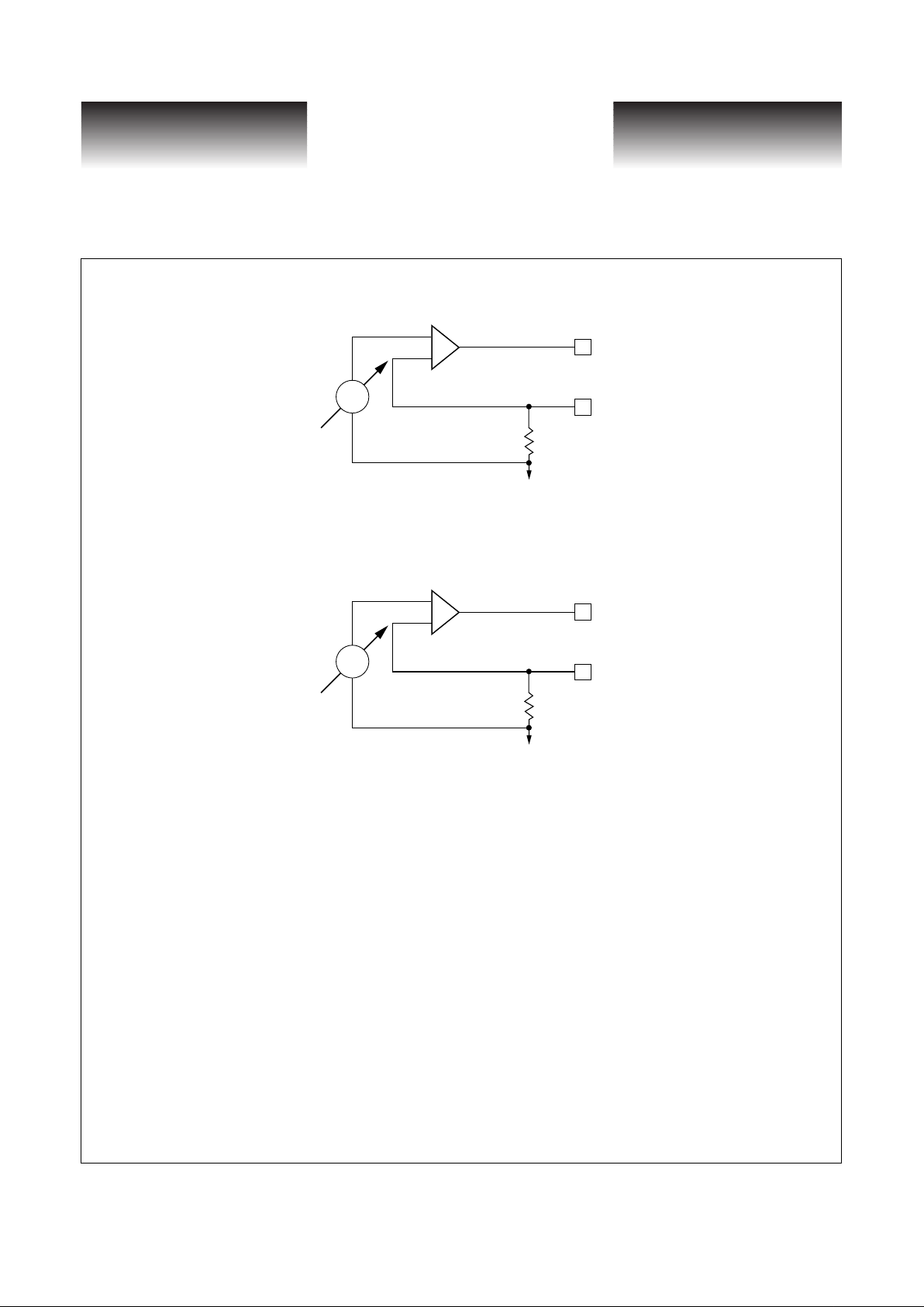
Figure 7: Differential Output Termination Methods
Table 3: Clock Multiplier Unit Performance
Parameter Description Min Typ Max Units Conditions
V
IH
Input HIGH voltage -1040 - -600 mV
Guaranteed HIGH
signal for all inputs
V
IL
Input LOW voltage V
TT
- -1600 mV
Guaranteed LOW
signal for all inputs
∆DIFF
IN
Differential input voltage
swing
0.400 0.800 1.4 V AC coupled
∆DIFF
OUT
Differential output voltage
swing
0.600 - - V See Figure 7
∆CM
OUT
Differential common mode
output voltage
VCC -
1.2V
See Figure 7
Name Description Min Typ Max Units
RC
d
Reference clock duty cycle 45 55 %
RCf Reference clock frequency 155.52 MHz
∆f
RC
Reference clock frequency range -100 +100 ppm
t
jitter
Jitter generation (12 KHz to 20 MHz) 0.01 UI
RMS
g
JT
Jitter transfer peaking 1.0 dB
f
-3dB
Jitter transfer -3dB bandwidth 1800 kHz
100Ω
~~
To
Receiver
VSC8161
50Ω
50Ω
~~
To
Receiver
VSC8161
GND
a) Two 50Ω resistors to a common AC ground b) 100Ω pad-pad termination
Termination Method (a) is preferred for improved noise immunity.
Page 8

Page 8 VITESSE
SEMICONDUCTOR CORPORATION
741 Calle Plano, Camarillo, CA 93012 • 805/388-3700 • FAX: 805/987-5896 8/28/98
VITESSE
SEMICONDUCTOR CORPORATION
Advance Product Information
VSC8161
.488Gb/s SONET / SDH
16:1 Mux with Clock Generator and Laser Driver
G52208-0, Rev.2.1
Table 4: Laser Driver AC Electrical Specifications
Table 5: Laser Driver DC Electrical Specifications
Power Dissipation
Table 6: Power Supply Currents and Power Dissipation
Note: Over recommended operating conditions, VCC = GND, outputs open-circuit)
a. I
BIAS
will be less than 2mA when (VIB - MIB) is less than 100mV.
b. I
MOD
will be less than 2mA when (VIP - MIP) is less than 100mV
Symbol Parameter Min Typ Max Units Conditions
tr, t
f
Output Rise and Fall Times 100 ps
25 Ohm Load, 10%-90%
15 mA < I
MOD
< 60 mA
I
BIAS
= 40 mA
Symbol Parameter Min Typ Max Units Conditions
I
BIAS
Programmable Laser Bias Current
a
50 mA
I
MOD
Programmable Modulation Current
b
60 mA
V
IB
Laser Bias Control Voltage VEE + 2.1 V
I
BIAS
= 50 mA
with 25Ω load
V
IP
Laser Modulation Control Voltage VEE + 2.1 V I
MOD
= 60 mA
V
OCM
Output Voltage Compliance VCC -2.5V V VEE = -5.2V
Parameter Description Typ Max Units
I
EE
Power supply current from VEE, max laser driver current 380 600 mA
I
TT
Power supply current from VTT, max laser driver current 210 300 mA
P
D
Power dissipation, max laser driver current 2.5 3.9 W
P
D
Power dissipation, min laser driver current 2.0 3.3 W
Page 9

VITESSE
SEMICONDUCTOR CORPORATION
Page 9
8/28/98 741 Calle Plano, Camarillo, CA 93012 • 805/388-3700 • FAX: 805/987-5896
VITESSE
SEMICONDUCTOR CORPORATION
Advance Product Information
SC8161
2.488Gb/s SONET / SDH
16:1 Mux with Clock Generator and Laser Driver
G52208-0, Rev.2.1
Absolute Maximum Ratings
(1)
Power Supply Voltage (VTT) ................................................................................................VCC-3.0V to VCC+0.5V
Power Supply Voltage (V
EE
) ..............................................................................................VCC-7.0V to VCC + 0.5V
Input Voltage Applied (V
VIN
) ............................................................................................... VTT-0.5V to VCC+0.5V
Output Current, I
OUT
(Modulation) .............................................................................................................. 60 mA
Output Current, I
OUT
(DC bias)....................................................................................................................50 mA
Case Temperature Under Bias (T
C
) ....................................................................................................-55o to 125oC
Junction T emperature (T
j
) ........................................................................................................... -55°C to + 125°C
Storage T emperature (T
STG
)..........................................................................................................-65
o
C to +150
o
C
Notes: (1) Caution: Stresses listed under “Absolute Maximum Ratings” may be applied to devices one at a time without causing
permanent damage. Functionality at or exceeding the values listed is not implied. Exposure to these values for extended
periods may affect device reliability.
(2) V
TT
must be applied before the magnitude of any input signal voltage (|VIN|, |V
HSIN
|) can be greater than |V
TT
- 0.5V|
Recommended Operating Conditions
Power Supply Voltage (VTT)....................................................................................................................-2.0V %
Power Supply Voltage (V
EE
)....................................................................................................................-5.2V %
Commercial Operating Temperature Range* (T)................................................................................... 0
o
to 85oC
* Specification limits are based upon case temperature.
5±
5±
Page 10

Page 10 VITESSE
SEMICONDUCTOR CORPORATION
741 Calle Plano, Camarillo, CA 93012 • 805/388-3700 • FAX: 805/987-5896 8/28/98
VITESSE
SEMICONDUCTOR CORPORATION
Advance Product Information
VSC8161
.488Gb/s SONET / SDH
16:1 Mux with Clock Generator and Laser Driver
G52208-0, Rev.2.1
VSC8161 Package Pin Diagram
1
2
3
4
5
6
7
8
10
11
12
13
14
15
17
18
19
20
21
22
23
24
25
16
9
NC
VEE
VCC
VEE
VCCANA
VEEANA
VEEANA
VCCANA
VTTANA
VCC
REFCK+
REFCK–
VTT
D0–
D1–
D1+
VCC
D2–
D2+
D3–
D3+
VTT
VSUB
D0+
NC
75
74
73
72
71
70
69
68
66
65
64
63
62
61
59
58
57
56
55
54
53
52
51
60
67
NC
NC
VEE
VCC
VEE
VCC
VTT
VTT
VCC
VTT
DINVALID+
DINVALID–
VTT
CLK16+
VTTHF
VCCHF
PARITY+
PARITY–
D15+
D15–
D14+
D14–
VCC
CLK16–
DINVERT
26272829303132
33
3536373839
40
424344454647484950
41
34
VTT
VCC
D4–
D4+
D5–
D5+
D6–
D6+
D7+
D8–
D8+
VTT
VCC
D9–
D10–
D10+
D11–
D11+
D12–
D12+
D13–
D13+
VTT
D9+
D7–
100999897969594
93
9190898887
86
848382818079787776
85
92
TEST2
VCC
VEE
VCCNCTEST1
TEST0
VCC
VCCO
IOUT–NCIOUT+
VCCO
MIP
MIB
VCC
VIB
VEEHF
VIP
VCCHFNCNC
VEE
VCC
VEE
Page 11

VITESSE
SEMICONDUCTOR CORPORATION
Page 11
8/28/98 741 Calle Plano, Camarillo, CA 93012 • 805/388-3700 • FAX: 805/987-5896
VITESSE
SEMICONDUCTOR CORPORATION
Advance Product Information
SC8161
2.488Gb/s SONET / SDH
16:1 Mux with Clock Generator and Laser Driver
G52208-0, Rev.2.1
Package Pin Description
Table 7: Pin Identification
Signal Name Pin # I/O Description
NC 1 - Do not connect, leave open
VEE 2 - SCFL negative supply (-5.2V typ.)
VCC 3 - Most positive supply (GND typ.)
VEE 4 - SCFL negative supply (-5.2V typ.)
VCCANA 5 - Most positive supply for analog circuits (GND typ.)
VEEANA 6 - SCFL negative supply for analog circuits (-5.2 typ.)
VEEANA 7 - SCFL negative supply for analog circuits (-5.2 typ.)
VCCANA 8 - Most positive supply for analog circuits (GND typ.)
NC 9 - Do not connect, leave open
VTTANA 10 - DCFL negative supply for analog circuits (-2.0V typ.)
VCC 11 - Most positive supply (GND typ.)
REFCK+ 12 I 155 MHz Reference Clock (true)
REFCK- 13 I 155 MHz Reference Clock (complement)
VTT 14 - DCFL negative supply (-2.0V typ.)
D0- 15 I Low-speed Differential Parallel Data
D0+ 16 I Low-speed Differential Parallel Data
D1- 17 I Low-speed Differential Parallel Data
D1+ 18 I Low-speed Differential Parallel Data
VCC 19 - Most positive supply (GND typ.)
D2- 20 I Low-speed Differential Parallel Data
D2+ 21 I Low-speed Differential Parallel Data
D3- 22 I Low-speed Differential Parallel Data
D3+ 23 I Low-speed Differential Parallel Data
VTT 24 - DCFL negative supply (-2.0V typ.)
VSUB 25 - Substrate Voltage (connect to lowest supply voltage, i.e., VEE)
VTT 26 - DCFL negative supply (-2.0V typ.)
VCC 27 - Most positive supply (GND typ.)
D4- 28 I Low-speed Differential Parallel Data
D4+ 29 I Low-speed Differential Parallel Data
D5- 30 I Low-speed Differential Parallel Data
D5+ 31 I Low-speed Differential Parallel Data
D6- 32 I Low-speed Differential Parallel Data
D6+ 33 I Low-speed Differential Parallel Data
D7- 34 I Low-speed Differential Parallel Data
D7+ 35 I Low-speed Differential Parallel Data
D8- 36 I Low-speed Differential Parallel Data
Page 12

Page 12 VITESSE
SEMICONDUCTOR CORPORATION
741 Calle Plano, Camarillo, CA 93012 • 805/388-3700 • FAX: 805/987-5896 8/28/98
VITESSE
SEMICONDUCTOR CORPORATION
Advance Product Information
VSC8161
.488Gb/s SONET / SDH
16:1 Mux with Clock Generator and Laser Driver
G52208-0, Rev.2.1
D8+ 37 I Low-speed Differential Parallel Data
VTT 38 - DCFL negative supply (-2.0V typ.)
VCC 39 - Most positive supply (GND typ.)
D9- 40 I Low-speed Differential Parallel Data
D9+ 41 I Low-speed Differential Parallel Data
D10- 42 I Low-speed Differential Parallel Data
D10+ 43 I Low-speed Differential Parallel Data
D11- 44 I Low-speed Differential Parallel Data
D11+ 45 I Low-speed Differential Parallel Data
D12- 46 I Low-speed Differential Parallel Data
D12+ 47 I Low-speed Differential Parallel Data
D13- 48 I Low-speed Differential Parallel Data
D13+ 49 I Low-speed Differential Parallel Data
VTT 50 - DCFL negative supply (-2.0V typ.)
VCC 51 - Most positive supply (GND typ.)
D14- 52 I Low-speed Differential Parallel Data
D14+ 53 I Low-speed Differential Parallel Data
D15- 54 I Low-speed Differential Parallel Data
D15+ 55 I Low-speed Differential Parallel Data
PARITY- 56 I Parity Bit (complement)
PARITY+ 57 I Parity Bit (true)
VCCHF 58 - Most positive supply for high frequency outputs (GND typ.)
VTTHF 59 - DCFL negative supply for high frequency outputs (-2.0V typ.)
CLK16- 60 O Low-speed clock f = 155.52 MHz (complement)
CLK16+ 61 O Low-speed clock f = 155.52 MHz (true)
VTT 62 - DCFL negative supply (-2.0V typ.)
DINVALID- 63 O Data Not Valid (complement)
DINVALID+ 64 O Data Not Valid (true)
VTT 65 - DCFL negative supply (-2.0V typ.)
VCC 66 - Most positive supply (GND typ.)
DINVERT 67 I Invert Data Output (Logic High = Invert)
VTT 68 - DCFL negative supply (-2.0V typ.)
VTT 69 - DCFL negative supply (-2.0V typ.)
VCC 70 - Most positive supply (GND typ.)
VEE 71 - SCFL negative supply (-5.2V typ.)
VCC 72 - Most positive supply (GND typ.)
VEE 73 - SCFL negative supply (-5.2V typ.)
NC 74 - Do not connect, leave open
NC 75 - Do not connect, leave open
Signal Name Pin # I/O Description
Page 13

VITESSE
SEMICONDUCTOR CORPORATION
Page 13
8/28/98 741 Calle Plano, Camarillo, CA 93012 • 805/388-3700 • FAX: 805/987-5896
VITESSE
SEMICONDUCTOR CORPORATION
Advance Product Information
SC8161
2.488Gb/s SONET / SDH
16:1 Mux with Clock Generator and Laser Driver
G52208-0, Rev.2.1
VEE 76 - SCFL negative supply (-5.2V typ.)
NC 77 - Do not connect, leave open
NC 78 - Do not connect, leave open
VCCHF 79 - Most positive supply for high frequency outputs (GND typ.)
VIP 80 I Laser Driver Modulation Current Control Node
VEEHF 81 - SCFL negative supply for high frequency outputs (-5.2 typ.)
VIB 82 I Laser Driver Bias Current Control Node
VCC 83 - Ext. current return path for bias and modulation control (GND typ.)
MIB 84 - Laser Driver Bias Current Source Monitor Node
VCC 85 - Ext. current return path for bias and modulation control (GND typ.)
MIP 86 - Laser Driver Modulation Current Source Monitor Node
VCCO 87 - Ext. current return path for IOUT+/- (GND typ.)
IOUT+ 88 O High-speed Data Out (true)
NC 89 - Do not connect, leave open
IOUT- 90 O High-speed Data Out (complement)
VCCO 91 - Ext. current return path for IOUT+/- (GND typ.)
VEE 92 - SCFL negative supply (-5.2V typ.)
VCC 93 - Most positive supply (GND typ.)
TEST0 94 - Connect to most positive supply (GND typ.)
TEST1 95 - Connect to most positive supply (GND typ.)
NC 96 - Do not connect, leave open
VCC 97 - Most positive supply (GND typ.)
VEE 98 - SCFL negative supply (-5.2V typ.)
VCC 99 - Most positive supply (GND typ.)
TEST2 100 - Connect to most positive supply (GND typ.)
Signal Name Pin # I/O Description
Page 14

Page 14 VITESSE
SEMICONDUCTOR CORPORATION
741 Calle Plano, Camarillo, CA 93012 • 805/388-3700 • FAX: 805/987-5896 8/28/98
VITESSE
SEMICONDUCTOR CORPORATION
Advance Product Information
VSC8161
.488Gb/s SONET / SDH
16:1 Mux with Clock Generator and Laser Driver
G52208-0, Rev.2.1
Table 8: Power Supply Summary
All supplies which reference the same voltage may be connected to the same power supply plane. The
VCCANA, VTTANA, and VEEANA are noise sensitive supplies, while the VCCHF, VCCO, VTTHF, and
VEEHF are noise generating supplies. Appropriate power supply noise suppression should be applied to optimize the performance of the device.
Signal Name Pin # Description
VEE 2,4,71,73,76,92,98 SCFL negative supply (-5.2V typ.)
VEEANA 6,7 SCFL negative supply for analog circuits (-5.2 typ.)
VEEHF 81 SCFL negative supply for high frequency outputs (-5.2 typ.)
VTT
14,24,26,38,50,62,65,
68,69
DCFL negative supply (-2.0V typ.)
VTTANA 10 DCFL negative supply for analog circuits (-2.0V typ.)
VTTHF 59 DCFL negative supply for high frequency outputs (-2.0V typ.)
VCC
3,11,19,27,39,51,66,70,
72,83,85,93,97,99
Most positive supply (GND typ.)
VCCANA 5,8 Most positive supply for analog circuits (GND typ.)
VCCHF 58,79 Most positive supply for high frequency outputs (GND typ.)
VCCO 87,91 Ext. current return path for IOUT+/- (GND typ.)
VSUB 25 Substrate Voltage (connect to lowest supply voltage, i.e., VEE)
TEST[0:2] 94,95,100 Connect to most positive supply (GND typ.)
Page 15

VITESSE
SEMICONDUCTOR CORPORATION
Page 15
8/28/98 741 Calle Plano, Camarillo, CA 93012 • 805/388-3700 • FAX: 805/987-5896
VITESSE
SEMICONDUCTOR CORPORATION
Advance Product Information
SC8161
2.488Gb/s SONET / SDH
16:1 Mux with Clock Generator and Laser Driver
G52208-0, Rev.2.1
Package Information
R
R
1
A
A
1
b
L
0.25
0.17 MAX
θ
6° ± 4°
10oTYP
10oTYP
A
2
e
A
E
E
1
D
D
1
HEATSINK INTRUSION
.0127 MAX
EXPOSED HEATSINK
6.86 ±.50 DIA.
100 PQFP: (14 x 14 x 2.0 mm) Package Drawing (Top View)
NOTES:
(1) Drawings not to scale.
(2) All units in millimeters unless otherwise noted
Package #: 101-318-3
Issue #: 2
Key mm Tolerance
A 2.35 MAX
A1 0.25 MAX
A2 2.00 +.10/-.05
D 17.20 ±.25
D1 14.00 ±.10
E 17.20 ±.25
E1 14.00 ±.10
L .88 +.15/-.10
e .50 BASIC
b .22 ±.05
θ 0°-7°
R .30 TYP
R1 .20 TYP
Body +3.2mm Footprint
Page 16

Page 16 VITESSE
SEMICONDUCTOR CORPORATION
741 Calle Plano, Camarillo, CA 93012 • 805/388-3700 • FAX: 805/987-5896 8/28/98
VITESSE
SEMICONDUCTOR CORPORATION
Advance Product Information
VSC8161
.488Gb/s SONET / SDH
16:1 Mux with Clock Generator and Laser Driver
G52208-0, Rev.2.1
Notice
This document contains information about a product during its fabrication or early sampling phase of development. The information contained in this document is based on design targets, simulation results or early prototype test results. Characteristic data and other specifications are subject to change without notice. Therefore
the reader is cautioned to confirm that this datasheet is current prior to design or order placement.
Warning
Vitesse Semiconductor Corporation’s product are not intended for use in life support appliances, devices or
systems. Use of a Vitesse product in such applications without written consent is prohibited.
 Loading...