

Page 1
VITESSE
SEMICONDUCTOR CORPORATION
Data Sheet
SC8140
Transceiver with Integrated Clock Generator
2.48832Gb/s 16:1 SONET/SDH
Features
• 2.48832Gb/s 16-Bit Transceiver
• Targeted for SONET OC-48 / SDH STM-16
Applications
• LVPECL Low-Speed Interface
• On-chip PLL-Based Clock Generator
• High-Speed Clock Output With Power-Down
Option
• Supports Parity at the 16-Bit Parallel T ransmit
and Receive Interfaces
• Provides Equ ipment, Facilities an d Split Loopback Modes as well as Loop Timing Modes
• Loss of Signal (LOS) Detect input
• Meets Bellcore Jitter Performance Specifications
• Single +3.3V Supply
• 2.25 Watts Typical Power Dissipation
• Packages: 128-pin PQFP or 208-pin TBGA
General Description
The VSC8140 is a SONET/SDH compatible transceiver with integrated clock generator for use in SONET/
SDH systems operating at a 2.48832Gb/s data rate. The internal clock generator uses a Phase-Locked Loop
(PLL) to multiply either a 77.76MHz or 155.5 2MHz ref er ence cl ock in ord er to provi de t he 2.488 32GHz clo ck
for internal logic and output retiming. The 16-bit parallel interface incorporates an on-board FIFO eliminating
loop timing design issues by providing a flexible parallel timing a rchitecture. In addition, the dev ice provides
both facility and equipment loopback modes and two loop timing modes. The VSC8140 operates using a 3.3V
power supply, and is available in either a th ermally-enh anced 128-PQF P or a thermally- enhanced 208 -pin
TBGA package.
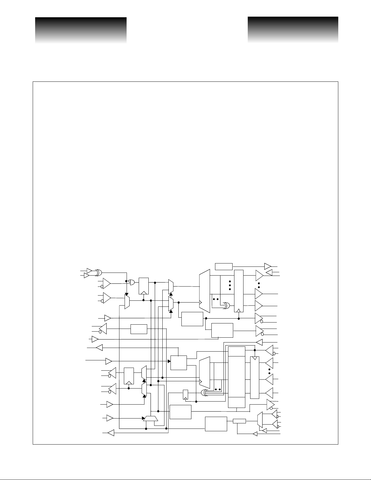
VSC8140 Block Diagram
LOS
POL
RXIN+
RXIN-
RXCLKIN+
RXCLKIN-
EQULOOP
CLK128O+
CLK128O-
RXCLKO_FREQSEL
OVERFLOW
FIFORESET
TXOUT+
TXOUT-
TXCLKOUT+
TXCLKOUT-
FACLOOP
LOOPTIM0
PARERR
Q D
Divide
by 128
D Q
Divide by
FIFO
CNTRL
Divide by
16
16
voltage
Divide by
2
2.48832GHz
PLL
gen.
Output Register
Write
Pointer
16x5 FIFO
Read
Pointer
VREFOUT
VREFIN
RXOUT0
RXOUT15
RXPARITYOUT
RXCLK16O+
RXCLK16O-
RXCLKO16_32+
RXCLKO16_32-
PARMODE
TXCLK16I+
TXCLK16I-
TXIN0
TXIN15
Input Register
TXPARITYIN
TXCLK16O+
TXCLK16O-
LPTIMCLK+
LPTIMCLK-
REFCLK+
REFCLK-
LOOPTIM1
REF_FREQSEL
G52251-0, Rev. 4.0
VITESSE SEMICONDUCTOR CORPORATION
9/6/00 741 Calle Plano, Camarillo, CA 93012 • 805/388-3700 • FAX: 805/987-5896
Page 1
Page 2
VITESSE
SEMICONDUCTOR CORPORATION
2.48832Gb/s 16:1 SONET/SDH
Transceiver with Integrated Clock Generator
Data Sheet
VSC8140
Functional Description
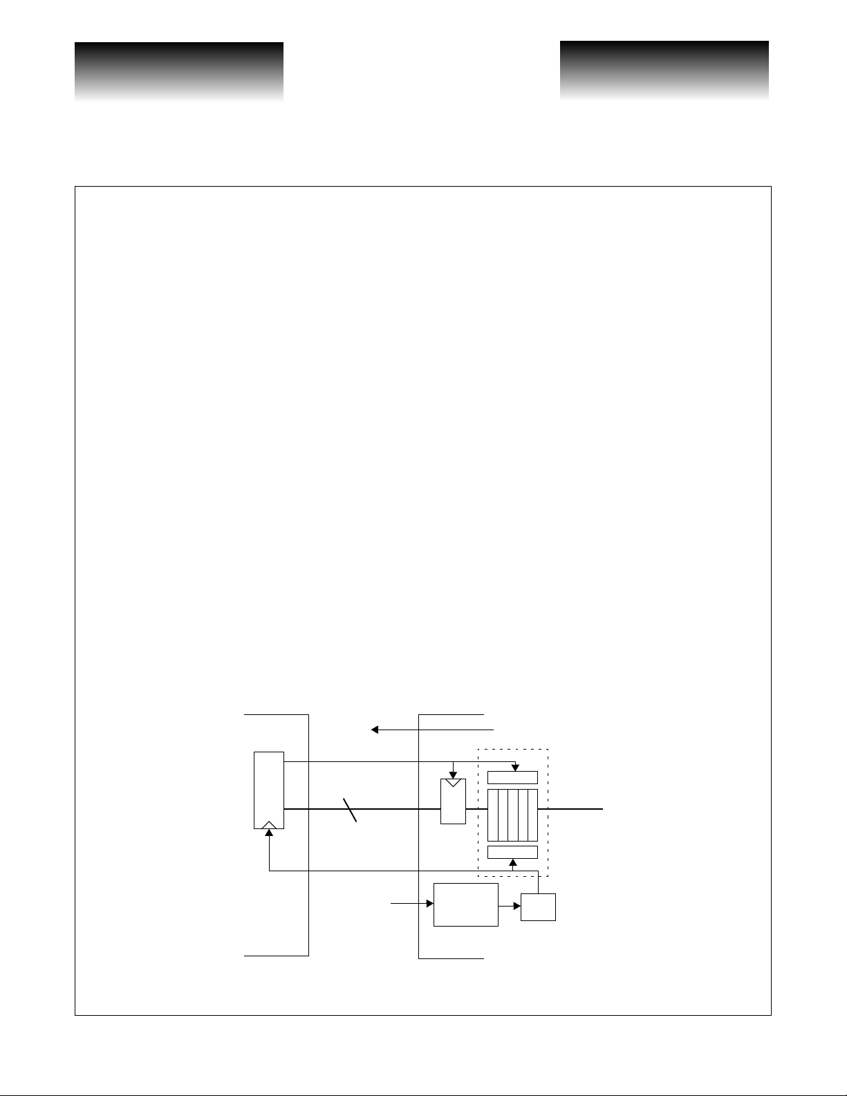
Transmitter Low-Speed Interface
The Upstream Device should use the TXCLK16O as the timing source for its final output latch (see Figure
1). The Upstream Device should then generate a TXCLK16I that is phase-aligned with the data. The VSC8140
will latch TXIN[15:0]
respect to TXCLK16I (see Table 1).
A FIFO exists within the VS C8140 to eliminate difficult system loop timing issues. O nce the PLL has
locked to the reference clock, RESET must be held low for a minimum of five CLK16 c ycles to initialize the
FIFO, then RESET should be set high and held constant for continuous FI FO operation. For the transpar ent
mode of operation (no FIFO), simply hold RESET at a constant low state (see Figure 2).
The use of a FIFO permits the system designer to tolerate an arbitrary amount of delay between
TXCLK16O and TXCLK16I. Once RESET is asserted and the FIFO initialized, the delay between TXCLK16O
and TXCLK16I can decrease or increase up to one period of th e low-spee d clock (6.4ns). Should this delay dri ft
exceed one period, the write pointer and the read pointer could point to the same word in the FIFO, resulting in
a loss of transmit ted d ata ( a F IFO o verf low ). In the e ven t of a FIF O ove rfl ow, an active low OV ERFLO W signal is asserted (for a minimum of five TXCLK16I cycles) which can be used to initiate a reset signal from an
external controller.
The TXCLK16O
transmission line can be DC termin ated wit h a spli t-end t erminat ion scheme (see F igure 3), or DC terminat ed by
50Ω to V
substituted for the traditional 50Ω to V
ods. Figure 5 illustrates an AC-coupling met hod for the occasi on when the downstr eam device provid es the bias
point for AC-coupling.
-2V on each line (see Figure 4). At any time, the equivalent split-end termination technique can be
CC
± on the rising edge of TXCLK16I+. The data must meet setu p and hold times with
± output driver is a LVPECL output driver designed to drive a 50
-2V on each line. AC-coupling can be ac hieved by a number of meth-
CC
transmission line. The
Ω
Page 2
741 Calle Plano, Camarillo, CA 93012 • 805/388-3700 • FAX: 805/987-5896 9/6/00
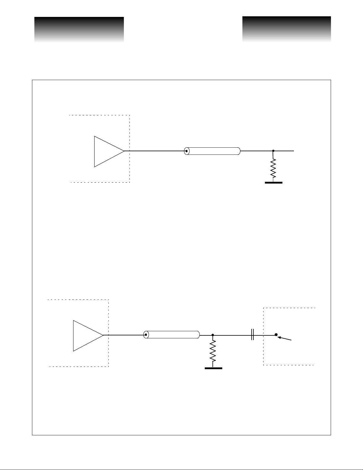
Figure 1: Low-Speed Systems Interface
OVERFLOW
TXCLK16I
16
TXCLK16O
REFCLK
VITESSE SEMICONDUCTOR CORPORATION
2.48832GHz
VSC8140
PLL
16 x 5 FIFO
write
read
Div 16
G52251-0, Rev. 4.0
Page 3
VITESSE
SEMICONDUCTOR CORPORATION
Data Sheet
SC8140
Transceiver with Integrated Clock Generator
Figure 2: Enabling FIFO Operation
2.48832Gb/s 16:1 SONET/SDH
PLL locked to reference clock.
Minimum 5 CLK16 cycles
RESET
Holding RESET “low” for a minimum of 5 CLK16 cycles, then setting “high” enables FIFO operation.
Holding RESET constantly “low” bypasses the FIFO for transparent mode operation.
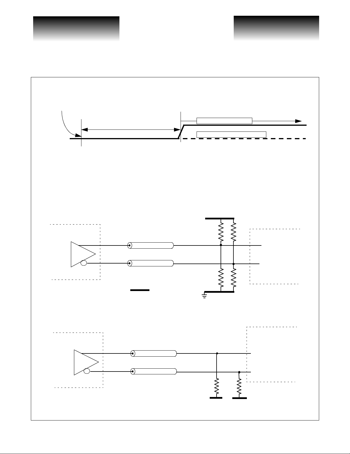
Figure 3: DC Termination of Low-Speed LVPECL RXCLK16O, RXCLK16_32O, TXCLK16O Outputs
VSC8140
Split-end equivalent termination is ZO to V
R1 = 125Ω R2 = 83Ω, ZO=50Ω, V
Z
o
TERM
TERM
= VCC-2V
FIFO Mode Operation
Transparen t M o de Operation
V
CC
R1
R1
downstream
Z
o
R1||R2 = Z
VCCR2 + VEER1
Figure 4: DC Termination of Low-Speed LVPECL RXCLK16O, RXCLK16_32O, TXCLK16O Outputs
R1+R2
O
= V
TERM
V
EE
R2
R2
downstream
VSC8140
G52251-0, Rev. 4.0
9/6/00 741 Calle Plano, Camarillo, CA 93012 • 805/388-3700 • FAX: 805/987-5896
VITESSE SEMICONDUCTOR CORPORATION
Z
o
R1 =50Ω
VCC-2V
R1 =50Ω
VCC-2V
Page 3
Page 4
VITESSE
SEMICONDUCTOR CORPORATION
2.48832Gb/s 16:1 SONET/SDH
Transceiver with Integrated Clock Generator
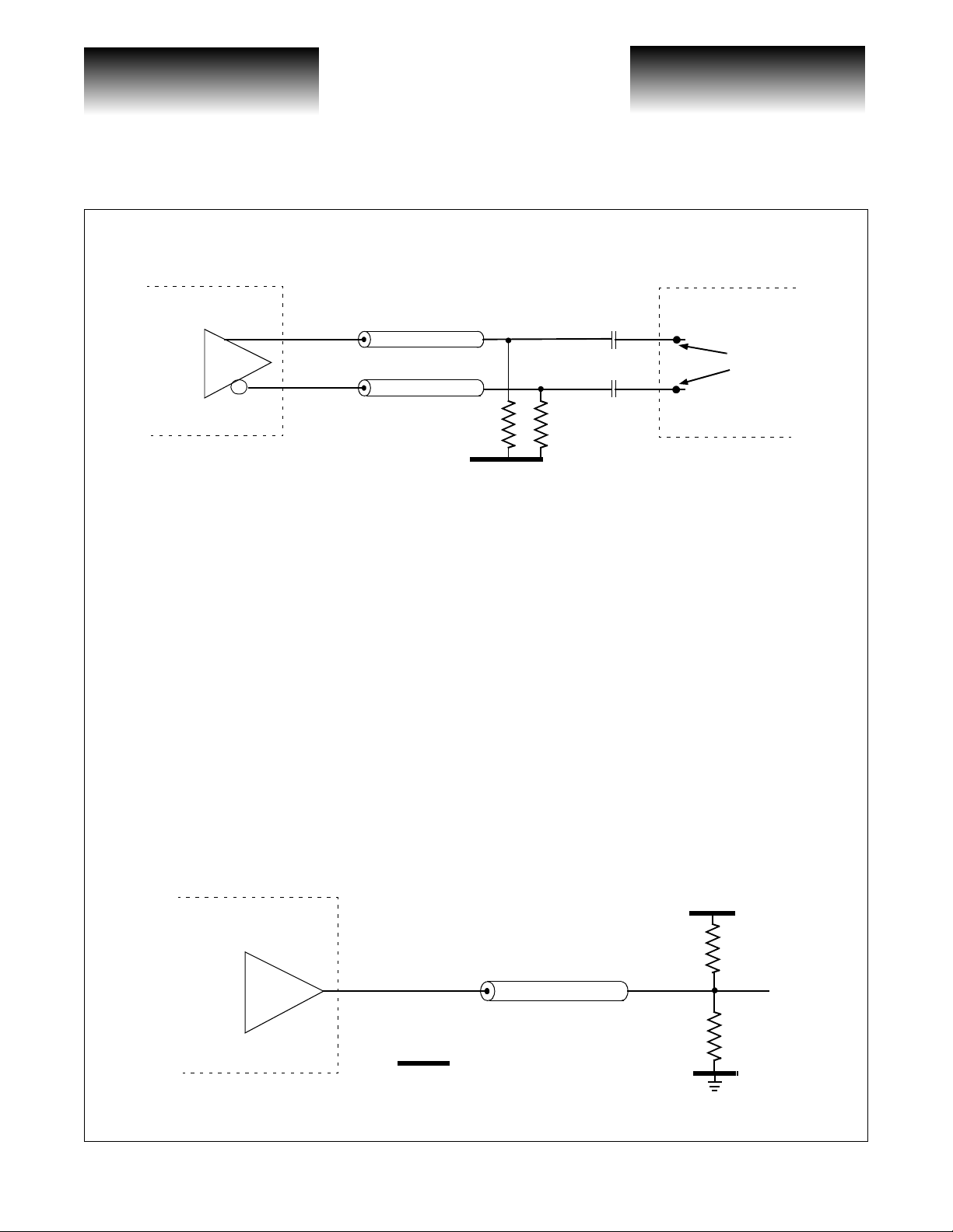
Figure 5: AC Termination of Low-Speed LVPECL RXCLK16O, RXCLK16_32O, TXCLK16O Outputs
VSC8140
Z
o
100nF
downstream
Data Sheet
VSC8140
bias point
generated
internally
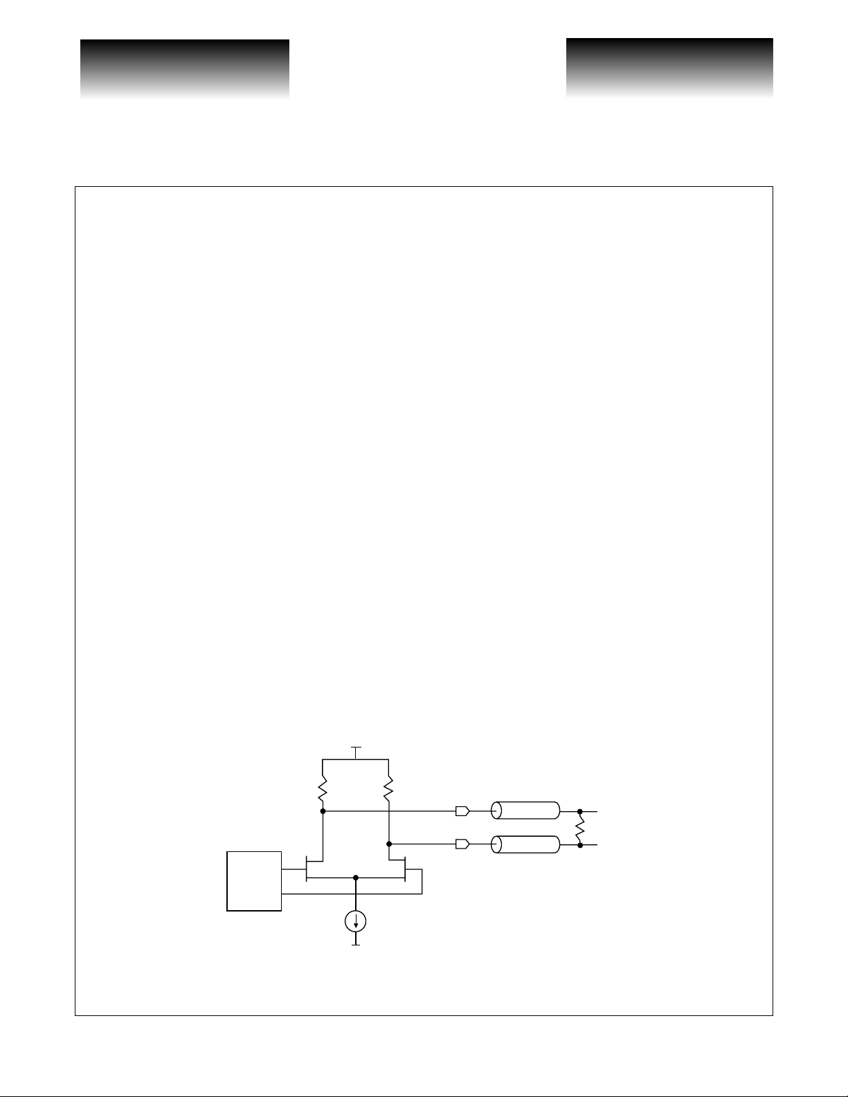
Receiver Low-Speed Interface
Z
o
100nF
50Ω
50Ω
V
CC
-2V
The demultiplexed serial stream is made available by a 16-bit single-ended LVPECL interface
RXOUT[15:0] with accompanying differential LVPECL divide-by-16 clock RXCLK16O
LVPECL divide-by-16 or -32 clock RXCLK16_32O
RXCLKO_FREQSEL is used to select RXCLK16_32O
RXCLK16_32O
± output as 77.76MHz, RXCLKO_FREQSEL = “1” designates RXCLK16_32O± output as
±.
±. RXCLKO_FREQSEL = “0” designates
± and selectable
155.52MHz.
The RXCLK16O and RXCLK1 6_32O outp ut drivers ar e designe d to drive a 5 0Ω transmission line. The
transmission line can be DC termin ated wit h a spli t-end t erminat ion scheme (see F igure 3), or DC terminat ed by
50Ω to V
-2V on each line (see Figure 4). A C-coupling can be achieved by a number of m ethods. Figure 5
CC
illustrates an AC-coupling method for the occasion when the downstream device provides the bias point for
AC-coupling. The divide-by-16 output (RXCLK16O) or the divide-by-16 or -32 output (RXCLK16_32O) can
be used to provide an external looptiming reference clock (after external filtering with a 1x REFCLK PLL) for
the clock multiplication unit on the VSC8140.
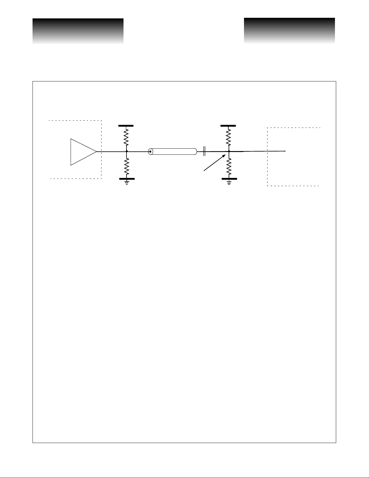
The RXOUT[15:0] output drivers are designed to drive a 50Ω transmission line which can be DC terminated with a split-end termination scheme (see Figure 6), or a traditional termination scheme (see Figure 7).
Figure 6: Split-end DC Termination of Low-Speed LVPECL RXOUT[15:0] Outputs
VSC8140
Page 4
741 Calle Plano, Camarillo, CA 93012 • 805/388-3700 • FAX: 805/987-5896 9/6/00
Split-end equivalent termination is ZO to V
R1 = 125Ω R2 = 83Ω, ZO=50Ω, V
R1||R2 = Z
V
CC
VITESSE SEMICONDUCTOR CORPORATION
o
R2 + VEER1
R1+R2
= V
TERM
TERM
Z
TERM
= VCC-2V
R1 = 125Ω
o
V
CC
R2 = 83Ω
V
EE
G52251-0, Rev. 4.0
Page 5
VITESSE
SEMICONDUCTOR CORPORATION
Data Sheet
SC8140
Figure 7: Traditional DC Termination of Low-Speed LVPECL RXOUT[15:0] Outputs
Transceiver with Integrated Clock Generator
2.48832Gb/s 16:1 SONET/SDH
VSC8140
Z
o
R1 =50Ω
VCC-2V
The RXOUT[15:0] outp ut drivers ca n also be ap propriate ly AC-co upled by a number of m ethods, ho wever, DC-coupling is preferred since there is no guarantee of transition density for individual bits in the 16-bit
word. Figure 8 illustrates an AC-coupling method for the occasion when the downs tream device pro vides the
bias point for AC-coupling. Figure 9 illustrates an AC-coupling method for the occasion when the bias point
needs to be generated externally. The resistor values in Figure 9 were selected to generate a bias point of 1.98V,
the mid-point for LVPECL V
generate the necessary bias point for the downstream device.
and VOL as specified for the VSC8140. Resistor values should be selected to
OH
Figure 8: AC Termination of Low-Speed LVPECL RXOUT[15:0] Outputs
VSC8140
Z
o
100nF
R1 = 50Ω
VCC-2V
G52251-0, Rev. 4.0
9/6/00 741 Calle Plano, Camarillo, CA 93012 • 805/388-3700 • FAX: 805/987-5896
VITESSE SEMICONDUCTOR CORPORATION
downstream
bias point
generated
internally
Page 5
Page 6
VITESSE
SEMICONDUCTOR CORPORATION
2.48832Gb/s 16:1 SONET/SDH
Transceiver with Integrated Clock Generator
Figure 9: AC Termination of Low-Speed LVPECL RXOUT[15:0] Outputs
V
CC
V
CC
Data Sheet
VSC8140
VSC8140
R1 = 125Ω
Z
o
100nF
R2 = 83Ω
bias point
V
EE
Parity
Systems employing internal parity are supported by the VSC8140. On the transmit side, a parity check is
performed between the TXPARITYIN input and the 16 TXIN[15:0] bits.
PARM ODE is use d to selec t even or odd parity expected for these 17 b its. (TXIN[ 15:0] an d TXPARI-
TYIN). PARMODE = “0” selects odd, PARMODE = “1” selects even. The PARERR output (parity error output) is asserted active high when the parity of the 17 bits (TXIN[15:0] and TXPARITYIN) does not conform to
the expected parity designated by PARMODE. PARERR becomes available T
TXCLK16I. PARERR is a NRZ pulse that is updated every 6.4 ns, i.e., the period of TXCLK16I. The timing
relationship of PARERR to TXCLK16I is shown in Figure 17. The PARERR pin may be left open if parity is
unused.
On the receive side, the parity output (RXPARITYOUT) is simply the XOR of all 16 outputs.
generated
externally
V
EE
R3 =83Ω
R4 = 125Ω
DV
downstream
after the rising edge of
Loss of Signal
The VSC8140 has a TTL input LOS to force the part into a Loss of Signal (LOS) state. Most optics have a
TTL output usually called Signal Detect (SD), based on the optical power of the incoming light stream.
Depending on the optics manufacturer, this signal is either active high or low. To accommodate polarity differences, the internal Loss of Sign al is generated when the POL and LOS i nputs a re of o pposit e states. Once acti ve,
all zeroes “0” will be propagated downstream u sing the transmit clock until the optical signal is regained and
LOS and POL are in the same logic state.
Page 6
741 Calle Plano, Camarillo, CA 93012 • 805/388-3700 • FAX: 805/987-5896 9/6/00
VITESSE SEMICONDUCTOR CORPORATION
G52251-0, Rev. 4.0
Page 7
VITESSE
SEMICONDUCTOR CORPORATION
Data Sheet
SC8140
Transceiver with Integrated Clock Generator
2.48832Gb/s 16:1 SONET/SDH
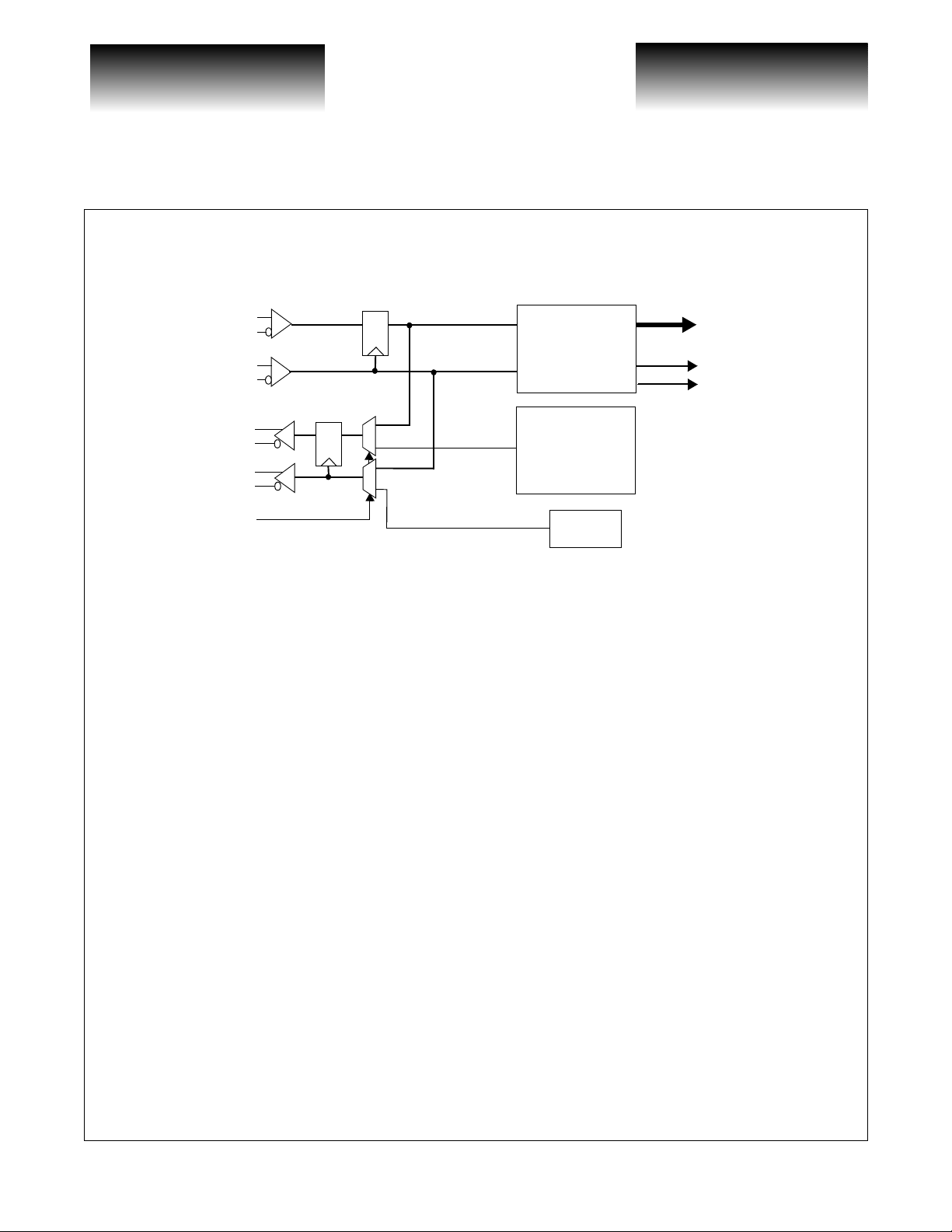
Figure 10: Facility Loopback Data Path
RXIN+
RXIN-
RXCLKIN+
RXCLKIN-
TXOUT+
TXOUT-
TXCLKOUT+
TXCLKOUT-
FACLOOP
Q D
D Q
1
0
1
0
1:16 Serial to
Parallel
16:1 Parallel to
Serial
2.48832GHz
PLL
RXOUT[15:0]
RXCLK16O
RXCLK32O
Facility Loopback
The facility loopback function is controlled by the FACLOOP signal. When the FACLOOP signal is set
high, the Facility Loopback mode is activated and the high-speed serial receive data (RXIN) is presented at the
high-speed transmit output (TXOUT), as depicted in Figure 10. In addition, the high-speed receive clock input
(RXCLKI) is selected and presented at the high-speed transmit clock output (TXCLKOUT). In Facility Loopback mode, the high-speed receive data (RXI N) is also convert ed to paral lel data and pr esented at the low-sp eed
receive output pins (RXOUT[15:0]). The receive clock (RXCLKIN) is also divided down and presented at the
low-speed clock output (RXCLK16O).
Equipment Loopback Data Path
The Equipment Loopback function is controlled by the EQULOOP signal, which is active high. When the
Equipment Loopback mode is activated, the high-speed transmit data generated from the parallel to serial conversion of the low-speed data (TXIN[15:0]) is selected and converted back to parallel data in the receiver section and presented at the low-speed parallel data outputs (RXOUT[15:0]), as shown in Figure 11. The internally
generated OC-48 clock is used to generate the low-speed receive output clocks (RXCLK16O and
RXCLK16_32O). In Equipment Loopback mode, the transmit data (TXIN[15:0]) is serialized and presented at
the high-speed output (TXOUT) along with the high-speed transmit clock (TXCLKOUT) which is generate d by
the on-chip PLL.
G52251-0, Rev. 4.0
9/6/00 741 Calle Plano, Camarillo, CA 93012 • 805/388-3700 • FAX: 805/987-5896
VITESSE SEMICONDUCTOR CORPORATION
Page 7
Page 8
VITESSE
SEMICONDUCTOR CORPORATION
2.48832Gb/s 16:1 SONET/SDH
Transceiver with Integrated Clock Generator
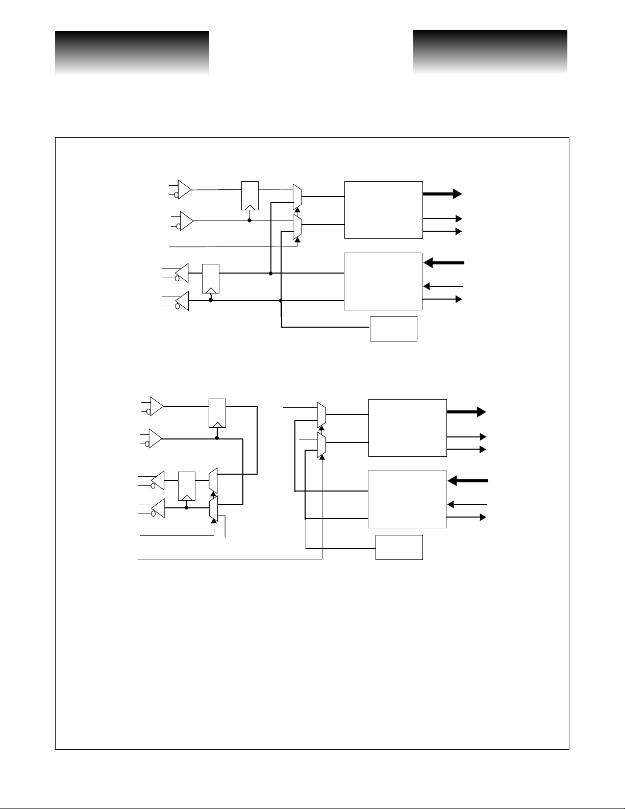
Figure 11: Equipment Loopback Data Path
EQULOOP
TXCLKOUT+
TXCLKOUT-
RXIN+
RXIN-
RXCLKIN+
RXCLKIN-
RXIN+
RXIN-
RXCLKIN+
RXCLKIN-
TXOUT+
TXOUT-
Q D
D Q
D Q
Figure 12: Split Loopback Datapaths
Data Sheet
VSC8140
0
1
0
1
0
1
0
1
1:16 Serial to
Parallel
16:1 Parallel to
Serial
2.48832GHz
PLL
1:16 Serial to
Parallel
RXOUT[15:0]
RXCLK16O
RXCLK32O
TXIN[15:0]
TXCLK16I
TXCLK16O
RXOUT[15:0]
RXCLK16O
RXCLK32O
TXOUT+
TXOUT-
TXCLKOUT+
TXCLKOUT-
FACLOOP
EQULOOP
Q D
1
0
1
0
16:1 Parallel to
Serial
2.48832GHz
PLL
TXIN[15:0]
TXCLK16I
TXCLK16O
Split Loopback
Equipment and Facility Loop back modes can b e enabled simultaneou sly. In this case, high-speed serial data
received (RXIN) and clock (RXCLKIN) are muxed through to the high-speed serial outputs (TXOUT and
TXCLKOUT). The low-speed 16-bit transmit stream (TXIN[15:0]) is muxed into the low-speed 16-bit receive
output stream (RXOUT[15:0]). See Figure 12.
Looptiming
LOOPTIM0 mode bypasses the PLL when LOOPTIM0 is asserted high. In this mod e, the PL L is by passed
using the receive high-speed clock (RXCLKIN), and the entire part is synchronously clocked from a single
external source.
Page 8
741 Calle Plano, Camarillo, CA 93012 • 805/388-3700 • FAX: 805/987-5896 9/6/00
VITESSE SEMICONDUCTOR CORPORATION
G52251-0, Rev. 4.0
Page 9
VITESSE
SEMICONDUCTOR CORPORATION
Data Sheet
SC8140
When LOOPTIM1 is asserted high, the RXCLK16_32O or RXCLK16O output can be tied to the LPTIMCLK input. In order to meet jitter transfer, the RXCLK16_32O or RXCLOCK16O needs to be filtered by a 1X
PLL circuit with a narrow pass characteristic. The part is forced out of this m ode in Equipment Loo pback to
prevent the PLL from feeding its own clock back.
Clock Generator
An on-chip PLL generates the 2 .48832GHz transmit c lock from the ex ternally provided REF CLK input.
The on-chip PLL uses a low phase noise reactance-based Voltage Controlled Oscillator (VCO) with an on-chip
loop filter (with two external 0.1µF peaking ca pacito rs). Th e loop ban dwi dth of th e PL L is wi thin t he SO NET
specified limit of 2MHz.
The customer can select to pr ovide either a 77. 76MHz reference, or 2x of that refer ence, 155.52MHz.
REF_FREQSEL is used to select the desired reference frequency. REF_FREQSEL = “0” designates REFCLK
input as 77.76MHz, REF_FREQSEL = “1” designates REFCLK input as 155.52MHz.
The REFCLK should be of high quality since noise on the REFCLK below the loop bandwidth of the PLL
will pass through the PLL and appear as jitter on the output. Preconditioning of the REFCLK signal with a
VCXO may be required to avoid passing REFCLK noise with greater than 2ps RMS of jitter to the output. The
VSC8140 will output the REFC LK noise in addit ion to the intrinsic jitter from the VSC 8140 itse lf during such
conditions.
Transceiver with Integrated Clock Generator
2.48832Gb/s 16:1 SONET/SDH
Loop Filter
The PLL on the VSC8140 employs a n inte rnal lo op fi lter wit h of f -chip pea kin g capaci tors. The PL L desi gn
is fully differential, therefore the loop filter must also be fully differential. One capacitor should be connected
between FILTAO and FILTAI, with the other connected between FILTAON and FILTAIN. Recommended
capacitors are low-inductance 0.1µF 0603 ceramic SMT X7R devices with a voltage rating equal to or greater
than 10V.
Figure 13: High-Speed Output Termination
V
CC
50Ω
100Ω
Z0 = 50Ω
Pre-Driver
50Ω
V
EE
G52251-0, Rev. 4.0
9/6/00 741 Calle Plano, Camarillo, CA 93012 • 805/388-3700 • FAX: 805/987-5896
VITESSE SEMICONDUCTOR CORPORATION
Page 9
Page 10
VITESSE
SEMICONDUCTOR CORPORATION
2.48832Gb/s 16:1 SONET/SDH
Transceiver with Integrated Clock Generator
Transmitter High-Speed Data and Clock Outputs
Data Sheet
VSC8140
The high-speed data and cloc k output drivers (TXOUT and TXCLKOUT) consist of a differential pair
designed to drive a 50Ω transmission line. The transmission line should be terminated with a 100Ω resistor at
the load between true and complement outputs (see Figure 13). No connection to a termination voltage is
required. The output driver is back terminated to 50Ω on-chip, providing a snubbing of any reflections. If used
single-ended, the high-speed outpu t driver must sti ll be termi nated dif feren tial ly at the l oad with a 100Ω resistor
between true and complement outputs.
In order to save power, the high-speed transmit clock output (TXCLKOUT) can be powered down by connecting the power pins VEEP_CLK and VEE_PWRDN to the V
Figure 14: AC Termination of Low-Speed LVPECL REFCLK and LPTIMCLK Inputs
Chip Boundary
VCC = 3.3V
V
CC
R1
Z
O
C
IN
supply instead of to VEE.
CC
R1||R2 = Zo , R1 = 83Ω R2 =125Ω
VCCR2 + VEER1
R1+R2
= V
BIAS
EE
CC
C
EE
R2
R1
IN
R2
= 0V
V
EE
CIN TYP = 100nF
for AC operation
V
V
Z
O
V
Reference Clock Inputs
The incoming low-speed reference clock inputs are rece ived by differential LVPECL inputs REFCLK± .
Off-chip termination of these inputs is required (see Figure 14).
In most situations these inputs will have high transition density and little DC offset. However, in cases
where this does not hold, direct DC connection is possible. All serial clock inputs have the same circuit topology, as shown in Figure 14. If the input signal is driven differentially and DC-coupled to the part, the mid-point
of the input signal swing should be centered about the input comm on-mode voltage V
and not exceed the
CM
maximum allowable amplitude. For single -ended , DC-coupling operat ions, it is re commended tha t the user provides an external reference voltage. The external reference should have a nominal value equivalent to the common-mode switch point of the DC-coupled signal, and can be connected to either side of the differential gate.
Page 10
741 Calle Plano, Camarillo, CA 93012 • 805/388-3700 • FAX: 805/987-5896 9/6/00
VITESSE SEMICONDUCTOR CORPORATION
G52251-0, Rev. 4.0
Page 11
VITESSE
SEMICONDUCTOR CORPORATION
Data Sheet
SC8140
Z
O
VREFIN
VREFOUT
2.48832Gb/s 16:1 SONET/SDH
Transceiver with Integrated Clock Generator
Figure 15: Termination of Low-Speed LVPECL TXIN[15:0] Inputs
Chip Boundary
VCC = 3.3V
V
CC
R1
C
IN
EE
R2
= 0V
V
EE
V
R1||R2 = Zo , R1 = 83Ω R2 =125Ω
VCCR2 + VEER1
R1+R2
= V
CIN TYP = 100nF
for AC operation
BIAS
Low-Speed Inputs
The incoming low-speed inputs are received by single-ended LVPECL inputs TXIN[15:0]. A reference
voltage is necessary to provide for optimal switching of the inputs. The user can either provide an input voltage
reference from the upstream de vice (VREFIN), or ca n use the reference volta ge provided from the VSC8140
(VREFOUT). Side-by-side placement of the VREFIN and VREFOUT pins facilitates easy implementation.
For DC or AC operation, the external reference should have a nominal value equivalent to the commonmode switch point of an LVPECL DC-coupled signal, and adhere to the DC characteristics as specified by the
Table 3 DC characteristics (V
G52251-0, Rev. 4.0
9/6/00 741 Calle Plano, Camarillo, CA 93012 • 805/388-3700 • FAX: 805/987-5896
).
CM
VITESSE SEMICONDUCTOR CORPORATION
Page 11
Page 12

VITESSE
SEMICONDUCTOR CORPORATION
2.48832Gb/s 16:1 SONET/SDH
Transceiver with Integrated Clock Generator
Figure 16: High-Speed Clock and High-Speed Data Inputs
Chip Boundary
1.65V
Z
O
V
TERM
Z
O
C
IN
C
AC
C
IN
50Ω
50Ω
3kΩ
3kΩ
VCC = 3.3V
VEE = 0V
3kΩ
3kΩ
Data Sheet
VSC8140
1.65V
TYP = 100nF
C
IN
C
TYP = 100nF
AC
High-Speed Clock and High-Speed Data Inputs
The incoming high-speed data and high-speed clock are received by high-speed inputs RXIN and
RXCLKIN. The inputs are internally biased to accommodate AC-coupling.
The data input receiver is internally terminated by a center-tapped resistor network. For differential input
DC-coupling, the network is terminated to the appropriate termination voltage V
providing a 50Ω to V
TERM
TERM
termination for both true and complement inputs. For differential input AC-coupling, the network is terminated
to V
via a blocking capacitor.
TERM
In most situations, these inputs will have high transition density and little DC offset. However, in cases
where this does not hold, direct DC connection is possible . All serial da ta and clo ck input s have the same circuit
topology, as shown in Figure 16. The reference voltage is created by a resist or divi der as shown. If the input signal is driven differentially and DC-coupled to the part, the mid-point of the input signal swing should be centered about this reference voltage and not exceed the maximum allowable amplitude. For single-ended, DCcoupling operations, it is reco mmended that th e user provide s an external referen ce voltage which has better
temperature and power supply noise rejection than the on-ch ip resistor divider. The external reference should
have a nominal value equivalent to the common-mode switch point of the DC-coupled signal, and can be connected to either sid e of the differential gate.
Page 12
741 Calle Plano, Camarillo, CA 93012 • 805/388-3700 • FAX: 805/987-5896 9/6/00
VITESSE SEMICONDUCTOR CORPORATION
G52251-0, Rev. 4.0
Page 13

VITESSE
SEMICONDUCTOR CORPORATION
Data Sheet
SC8140
Supplies
The VSC8140 is specified as a PECL device with a single positive 3.3V supply. Should the user desire to
use the device in an ECL environment with a negative 3.3V supply, then V
3.3V. If used with V
Decoupling of the power supplies is a critical element in maintaining the proper operation of the part. It is
recommended that the V
on each V
also be placed in parallel with the 0.1µF and 0.01µF capacitors mentioned above. Recommended capacitors are
low-inductance ceramic SMT X7R devices. For the 0.1µF capacitor, a 0603 package should be used. The
0.01µF and 0.001µF capacitors can be either 0603 or 0403 packages.
Extra care needs to be taken when decoupling the analog power supply pins (labeled V
maintain the optimal jitter and loop bandwidth characteristics of the PLL contained in the VSC8140, the analog
power supply pins sh ould be filtered fr om the ma in pow er supply w ith a 10µH C-L-C pi filter. If preferred, a
ferrite bead may be used to provide the isolation. The 0.1µF and 0.01µF decoupling capacitors are still required
and must be connected to the supply pins between the device and the C-L-C pi filter (or ferrite bead).
For low frequency decoupling, 47µF tantalum low-inductance SMT caps are sprinkled over the board’s
main +3.3V power supply and placed close to the C-L-C pi filter.
If the device is being used in an ECL environment with a -3.3V supply, then all references to decoupling
V
must be changed to VEE, and all references to decoupling 3.3V must be changed to -3.3V.
CC
power supply pin as close to the package as possible. If room permits, a 0.001µF capacitor should
CC
tied to -3.3V, the TTL control signals are still referenced to VEE.
EE
power supply be decoupled using a 0.1µF and 0.01µF capacitor placed in parallel
CC
Transceiver with Integrated Clock Generator
2.48832Gb/s 16:1 SONET/SDH
will be ground and VEE will be -
CC
). In order to
CCANA
Figure 17: PLL Power Supply Decoupling Scheme
10µH
V
EE
0.1µF 0.1µF
V
CC
Note: VCC can be tied to V
V
CCANA
0.01µF
V
CCANA
CCANA
V
EEANA
G52251-0, Rev. 4.0
9/6/00 741 Calle Plano, Camarillo, CA 93012 • 805/388-3700 • FAX: 805/987-5896
VITESSE SEMICONDUCTOR CORPORATION
Page 13
Page 14

VITESSE
SEMICONDUCTOR CORPORATION
2.48832Gb/s 16:1 SONET/SDH
Transceiver with Integrated Clock Generator
AC Characteristics
Figure 18: Transmitter Parallel Data Timing Waveforms
Parallel Data Clock Input
TXIN[0:15]+, TXPRTYIN
Parallel Data Clock Output
TXCLK16I+
Parallel Data Inputs
TXCLK16O+
t
TXDSU
t
TXDH
Valid Data 1
= don’t care
Figure 19: Transmitter Serial Data and Clock Phase Timing
Data Sheet
VSC8140
Valid Data 2
t
DH
Differential Serial Data Output
TXOUT+
TXCLKO+
Differential Clock Output
NOTE: Bit 15 (MSB) is transmitted first, Bit 0 (LSB) is transmitted last.
TXCLK16I+
Parallel Data Clock Input
PARERR+
Data Valid Output
D15
MSB
D14
t
PD
D13
Time
Figure 20: Transmitter Parity Timing
t
D
t
DV
t
D
D1 D0
LSB
Page 14
741 Calle Plano, Camarillo, CA 93012 • 805/388-3700 • FAX: 805/987-5896 9/6/00
VITESSE SEMICONDUCTOR CORPORATION
G52251-0, Rev. 4.0
Page 15

VITESSE
SEMICONDUCTOR CORPORATION
Data Sheet
SC8140
Transceiver with Integrated Clock Generator
2.48832Gb/s 16:1 SONET/SDH
Figure 21: Differential and Single-Ended Input / Output Voltage Measurement
b
a
b
Single
Ended
Swing
Differential
Swing
=
α
=
α
a
(α
* Differential swing
) is specified as | b - a | ( or | a - b | ), as is the single-ended swing.
Differential swing is specified as equal in magnitude to single-ended swing.
Table 1: Transmitter AC Characteristics
Parameters Description Min Typ Max Units Conditions
T
D
T
TXDSU
T
TXDH
T
T
TXCLK
t
t
TXCLK16O
TXCLK16I
RCK
T
t
t
Clock Multiplier Performan ce
T
T
Jitter
,
TXDOR
TXDOF
D
TXCLK16R
TXCLK16F
D
DV
DH
PD
DJ
CJ
tol
,
TXCLK16I/TXCLK16O period —6.4—ns—
Data setup time to the rising edge of
TXCLK16I+
Data hold time after the rising edge
of TXCLK16I+
TXOUT± rise and fall time — — 120 ps
Transmit clock duty cycle 40 — 60 % —
TXCLK16O± rise and fall times — — 250 ps See Figure 24
TXCLK16O± duty cycle 46 — 53 % —
D
TXCLK16I± duty cycle 35 — 65 %
D
Reference clock duty cycle 40 — 60 % —
Parallel data to DINVALID — 3 tD + 0.3 — ns —
TXCLKO period — 401.9 — ps —
Center of output data eye from
falling edge of TXCLKO
Output data jitter — — 4 ps
Output clock jitter — — 4 ps
Jitter tolerance — — — — Exceeds SONET/SDH mask
Tuning Range -100 +100 ppm
0.75 — — ns —
1.0 — — ns —
20% to 80% into 100Ω load.
See Figure 13.
Assuming 10% distortion of
TXCLK16O.
-75 — +75 ps See Figure 19
RMS, tested to SONET
specification (12kHz to
20MHz) with 2ps RMS jitter
on REFCLK.
RMS, tested to SONET
specification (12kHz to
20MHz) with 2ps RMS jitter
on REFCLK.
G52251-0, Rev. 4.0
9/6/00 741 Calle Plano, Camarillo, CA 93012 • 805/388-3700 • FAX: 805/987-5896
VITESSE SEMICONDUCTOR CORPORATION
Page 15
Page 16

VITESSE
SEMICONDUCTOR CORPORATION
2.48832Gb/s 16:1 SONET/SDH
Transceiver with Integrated Clock Generator
Figure 22: Receiver AC Timing Waveforms
Parallel Data Clock Output
Parallel Data Clock Output
Differential Serial Data Input
RXCLK16O+
RXOUT[0:15]+
Parallel Data Outputs
RXCLK32O+
Figure 23: Receiver Setup and Hold Time Requirements
RXIN+
t
RXDSU
Valid Data 1
= don’t care
t
RXDSU
D15
MSB
D14
t
RXDH
D13
t
RXPDD
t
RXPD32
Time
Data Sheet
VSC8140
Valid Data 2
D1 D0
LSB
Differential Clock Input
RXCLKIN+
NOTE: Bit 15 (MSB) is received first, Bit 0 (LSB) is received last.
Table 2: Receiver AC Charact eristics
Parameters Description Min Typ Max Units Conditions
t
RXPDD
t
RXPD32
t
, t
RXDR
RXDF
RXCLKR
RXCLKF
,
t
t
RXCLK16O
t
RXDSU
Data valid from falling edge of
RXCLK16O+
RXCLK32O transition from
falling edge of RXCLK16O+
RXOUT[15:0]+/- rise and fall
times
RXCLK16O+/- rise and fall
times
RXCLK16O+/- duty cycle
D
distortion
RXIN+ setup time with respect
to falling edge of RXCLKIN+
0 800 ps —
01.0ns—
— 300 ps
— 250 ps
45 55
% of
clock cycle
20% to 80% into DC termination.
See Figure 24.
20% to 80% into 100Ω load.
See Figure 24.
High-speed clock input at
2.48832GHz.
100 — ps —
RXIN+ hold time with
t
RXDH
respect to falling edge of
75 — ps
—
RXCLKIN+
RXCLKIN
RXCLKIN+/- duty cycle
D
distortion
40 60
% of
clock cycle
—
Page 16
741 Calle Plano, Camarillo, CA 93012 • 805/388-3700 • FAX: 805/987-5896 9/6/00
VITESSE SEMICONDUCTOR CORPORATION
G52251-0, Rev. 4.0
Page 17

VITESSE
SEMICONDUCTOR CORPORATION
Data Sheet
SC8140
DC Characteristics
Table 3: DC Characteristics
Parameters
V
OHHSO
V
OLHSO
∆V
V
CMHSO
R
HSO
∆V
V
OHL
V
OL
∆V
V
IH
V
IL
I
IH
I
IL
R
i
∆V
V
CM
V
OH
V
OL
V
IH
V
IL
I
IH
I
IL
V
CC
P
D
I
CC
ODHSO
IHS
O
I
Output HIGH voltage (TXOUT,
TXCLKOUT)
Output LOW voltage (TXOUT,
TXCLKOUT)
Output differential voltage
(TXCLKOUT)
Output differential voltage
(TXOUT)
Output common-mode voltage VCC-1.20 — VCC-0.300 V
Back termination impedance 40 — 60 Ω Guaranteed, but not teste d
Serial input differential voltage
(RXIN, RXCLKIN)
Output HIGH voltage (LVPECL) VCC-1.020 — VCC-0.700 V Se e Figure 24
Output LOW voltage (LVPECL) VCC-2.000 — VCC-1.620 V Se e Figure 24
Low-speed output vo ltage single-
ended, peak-to-peak swing
(LVPECL)
Input HIGH voltage (LVPECL) VCC-1.100 — VCC-0.700 V —
Input LOW voltage(LVPECL) VCC-2.0 — VCC-1.540 V —
Input HIGH current (LVPECL) — — 200 µA VIN=V
Input LOW current (LVPECL) -50 — — µA VIN=VIL(min)
Input Resistance (LVPECL) 10k — — Ω —
Input differe nti al vo lta ge
(LVPECL)
Input common-mode voltage
(LVPECL)
Output HIGH voltage (TTL) 2.4 — — V I
Output LOW voltage (TTL) — — 0.5 V I
Input HIGH voltage (TTL) 2.0 — 5.5 V —
Input LOW voltage (TTL) 0.0 — 0.8 V —
Input HIGH Current (TTL) — — 500 µA V
Input LOW current (TTL) — — -500 µA V
Supply voltage 3.14 — 3.47 V 3.3V± 5%
Power dissipation — 2.25 2.75 W Outputs op en
Supply current — — 800 mA Outputs open
2.48832Gb/s 16:1 SONET/SDH
Transceiver with Integrated Clock Generator
(Over recommended operating conditions)
Description Min Typ Max Units Conditions
V
-0.40 —VCCV50Ω termination to V
CC
V
-1.20 — VCC-0.50 V 50Ω termination to V
CC
450 600 1000
500 600 1000
200 — — mV
600 — 1300 mV See Figure 24
200 — — mV —
V
-1.5 — VCC-0.5 V —
CC
100Ω termination between ±
mV
output at load. See Figure 13.
100Ω termination between ±
output at load. See Figure 13.
AC-coupled, internally
biased to (V
(max)
IH
= -1.0mA
OH
= +1.0mA
OL
= 2.4V
IN
= 0.5V
IN
CC+VEE
CC
CC
)/2.
G52251-0, Rev. 4.0
9/6/00 741 Calle Plano, Camarillo, CA 93012 • 805/388-3700 • FAX: 805/987-5896
VITESSE SEMICONDUCTOR CORPORATION
Page 17
Page 18

VITESSE
SEMICONDUCTOR CORPORATION
2.48832Gb/s 16:1 SONET/SDH
Transceiver with Integrated Clock Generator
Figure 24: Parametric Measurement Information
PECL Rise and Fall Time
80%
20%
T
r
Absolute Maximum Ratings
Power Supply Voltage (VCC)...........................................................................................................-0.5V to +3.8V
DC Input Voltage (differential inputs).....................................................................................-0.5V to V
DC Input Voltage (TTL inputs).......................................................................................................-0.5V to +5.5V
DC Output Voltage (TTL outputs) .........................................................................................-0.5V to V
Output Current (TTL outputs).................................................................................................................. +/-50mA
Output Current (differential outputs).........................................................................................................+/-50mA
Case Temperature Under Bias......................................................................................................-55
T
f
(1)
Parametric Test Load Circuit
Serial Output Load
Z0 = 50Ω
Data Sheet
VSC8140
V
CC
o
C to +125oC
50Ω
-2V
CC
CC
+0.5V
+ 0.5V
Recommended Operating Conditions
Power Supply Voltage (VCC)..................................................................................................................+3.3V+5%
Operating Temperature Range ...........................................................0
NOTE: (1) CAUTION: Stresses listed under “Absolute Maximum Ratings” may be applied to devices one at a time without caus-
ing permanent damage. Functionality at or above the values listed is not implied. Exposure to these values for extended
periods may affect device reliability.
o
C Ambient to +110oC Case Temperature
ESD Ratings
Proper ESD procedures should be used when handling this product. The VSC8140 is rated to the following
ESD voltages based on the human body model:
1. All pins are rated at or above 1500V.
Page 18
741 Calle Plano, Camarillo, CA 93012 • 805/388-3700 • FAX: 805/987-5896 9/6/00
VITESSE SEMICONDUCTOR CORPORATION
G52251-0, Rev. 4.0
Page 19

VITESSE
SEMICONDUCTOR CORPORATION
Data Sheet
SC8140
Transceiver with Integrated Clock Generator
Package Pin Descriptions
Table 4: Package Pin Identification - 128 PQFP
Pin # Name I/O Level Description
1 OVERFLOW O TTL FIFO overflow indication
2VEET— GND typ. TTL VEE power supply
3 VCCT — +3.3V typ. TTL VCC power supply
4 VEE — GND typ. Negative power supply
5 HSDREF I 0V->3.3V High-speed data input termination voltage reference
6 VEE — GND typ. Negative power supply
7 RXIN+ I HS High-speed data input, true
8 RXIN- I HS High-speed data input, complement
9 VCC — 3.3V typ. Positive power supply
10 VEE — GND typ. Negative power supply
11 VEE — GND typ. Negative power supply
12 VCC — 3.3V typ. Positive power supply
13 RXCLKIN- I HS High-speed clock input, comple ment
14 HSCLKREF I 0V->3.3V High-speed clock input termination voltage reference
15 RXCLKIN+ I HS High-speed clock Input, true
16 VCC — 3.3V typ. Positive power supply
17 NC — — No connect, leave unconnected
18 VCC — 3.3V typ. Positive power supply
19 VCC — 3.3V typ. Positive power supply
20 TXOUT+ O HS High-speed data output, true
21 TXOUT- O HS High-speed data outpu t, complement
22 VCC — 3.3V typ. Positive power supply
23 VEE — GND typ. Negative power supply
24 VEE — GND typ. Negative power supply
25 VEE — GND typ. Negative power supply
26 VCC — 3.3V typ. Positive power supply
27 VCC — 3.3V typ. Positive power supply
28 TXCLKOUT+ O HS High-speed clock output, true
29 TXCLKOUT- O HS High-speed clock output, complement
30 VCC — 3.3V typ. Positive power supply
31 VEEP_CLK — GND typ. HS clock V
32 VEEP_CLK — GND typ. HS clock VEE power supply (tie to VCC for power down)
33 VEE_PWRDN I GND typ. HS clock VEE power supply (tie to VCC for power down)
34 VCC — 3.3V typ. Positive power supply
35 VCC — 3.3V typ. Positive power supply
36 VCC — 3.3V typ. Positive power supply
power supply (tie to VCC for power down)
EE
2.48832Gb/s 16:1 SONET/SDH
(1)
G52251-0, Rev. 4.0
9/6/00 741 Calle Plano, Camarillo, CA 93012 • 805/388-3700 • FAX: 805/987-5896
VITESSE SEMICONDUCTOR CORPORATION
Page 19
Page 20

VITESSE
SEMICONDUCTOR CORPORATION
2.48832Gb/s 16:1 SONET/SDH
Transceiver with Integrated Clock Generator
Table 4: Package Pin Identification - 128 PQFP
Pin # Name I/O Level Description
37 VEE — GND typ. Negative power supply
38 FACLOOP I TTL Facility loopback, active high
39 LOOPTIM0 I TTL Enable internal looptiming operation, active high
40 PARMODE I TTL Parity mode select
41 FIFORESET I TTL Reset to align FIFO write and read poin ters
42 LOOPTIM1 I TTL Enable external loop timing operation, active high
43 REF_FREQSEL I TTL Reference clock input select
44 LPTIMCLK+ I LVPECL External loop timing clock, true
45 LPTIMCLK- I LVPECL External loop timing clock, complement
46 VCC_ANA — +3.3V typ. Positive power supplys for analog parts of CMU
47 VEE_ANA — GND typ. Negative power supplys for analog parts of CMU
48 REFCLK+ I LVPECL Reference clock i nput, true
49 REFCLK- I LVPECL Reference clock input, complement
50 VEE — GND typ. Negative power supply
51 FILTAO — — Loop filter pin - connect via capacitor to FILTAI (pin 53)
52 FILTAON — — Loop filter pin - connect via capacitor to FILTAIN (pin 54)
53 FILTAI — — Loop filter pin - connect via capacitor to FILTAO (pin 51)
54 FILTAIN — — Loop filter pin - connect via capacitor to FILTAON (pin 52)
55 VCC — 3.3V typ. Positive power supply
56 TXCLK16O+ O LVPECL
57 TXCLK16O- O LV PECL
58 VEE — GND typ. Negative power supply
59 TXCLK16I- I LVPECL Low-speed clock input for latching low-speed data, complement
60 TXCLK16I+ I LVPECL Low-speed clock input for latching low-speed data, true
61 VCC — 3.3V typ. Positive power supply
62 TXPARITYIN I LVPECL Transmitter parity bit input
63 TXIN15 I LVPECL Low-speed single-ended data (MSB)
64 TXIN14 I LVPECL Low-speed single-ended data
65 VEE — GND typ. Negative power supply
66 VCC — 3.3V typ. Positive power supply
67 TXIN13 I LVPECL Low-speed single-ended data
68 TXIN12 I LVPECL Low-speed single-ended data
69 TXIN11 I LVPECL Low-speed single-ended data
70 TXIN10 I LVPECL Low-speed single-ended data
71 TXIN9 I LVPECL Low-speed single-ended data
Low-speed clock output, true. A divide-by-16 version of the PLL
clock.
Low-speed clock output, complement. A divide-by-16 version of the
PLL clock.
Data Sheet
VSC8140
(2)
Page 20
741 Calle Plano, Camarillo, CA 93012 • 805/388-3700 • FAX: 805/987-5896 9/6/00
VITESSE SEMICONDUCTOR CORPORATION
G52251-0, Rev. 4.0
Page 21

VITESSE
SEMICONDUCTOR CORPORATION
Data Sheet
SC8140
Table 4: Package Pin Identification - 128 PQFP
Pin # Name I/O Level Description
72 VEE — GND typ. Negative power supply
73 TXIN8 I LVPECL Low-speed single-ended data
74 TXIN7 I LVPECL Low-speed single-ended data
75 TXIN6 I LVPECL Low-speed single-ended data
76 TXIN5 I LVPECL Low-speed single-ended data
77 TXIN4 I LVPECL Low-speed single-ended data
78 VCC — 3.3V typ. Positive power supply
79 TXIN3 I LVPECL Low-speed single-ended data
80 TXIN2 I LVPECL Low-speed single-ended data
81 VEE — GND typ. Negative power supply
82 TXIN1 I LVPECL Low-speed single-ended data
83 TXIN0 I LVPECL Low-speed single-ended data (LSB)
84 VCC — 3.3V typ. Positive power supply
85 VREFIN I Voltage Voltage reference for single-ended TXIN V
86 VREFOUT O Voltage Voltage reference for single-ended RXOUT (VOH+VOL)/2.
87 VCC — 3.3V typ. Positive power supply
88 RXOUT0 O LVP ECL Low-speed single-ended data (LSB)
89 RXOUT1 O LVP ECL Low-speed single-ended data
90 VEE — GND typ. Negative power supply
91 RXOUT2 O LVP ECL Low-speed single-ended data
92 RXOUT3 O LVP ECL Low-speed single-ended data
93 VCC — 3.3V typ. Positive power supply
94 RXOUT4 O LVP ECL Low-speed single-ended data
95 RXOUT5 O LVP ECL Low-speed single-ended data
96 VCC — 3.3V typ. Positive power supply
97 RXOUT6 O LVP ECL Low-speed single-ended data
98 RXOUT7 O LVP ECL Low-speed single-ended data
99 VEE — GND typ. Negative power supply
100 RXOUT8 O LVPECL Low-speed single-ended data
101 RXOUT9 O LVPECL Low-speed single-ended data
102 VCC — 3.3V typ. Positive power supply
103 VCC — 3.3V typ. Positive power supply
104 RXOUT10 O LVPECL Low-spe ed single-ended data
105 RXOUT11 O LVPECL Low-speed single-ended data
106 RXOUT12 O LVPECL Low-spe ed single-ended data
107 VCC — 3.3V typ. Positive power supply
108 RXOUT13 O LVPECL Low-spe ed single-ended data
Transceiver with Integrated Clock Generator
2.48832Gb/s 16:1 SONET/SDH
(2)
or VREFOUT
CM
(2)
G52251-0, Rev. 4.0
9/6/00 741 Calle Plano, Camarillo, CA 93012 • 805/388-3700 • FAX: 805/987-5896
VITESSE SEMICONDUCTOR CORPORATION
Page 21
Page 22

VITESSE
SEMICONDUCTOR CORPORATION
2.48832Gb/s 16:1 SONET/SDH
Transceiver with Integrated Clock Generator
Table 4: Package Pin Identification - 128 PQFP
Pin # Name I/O Level Description
109 RXOUT14 O LVPECL Low-spe ed single-ended data
110 VEE — GND typ. Negative power supply
111 RXOUT15 O LVPECL Low-speed single-ended data (MSB)
112 RXPARITYOUT O LVPECL Receiver parity bit output
113 VCC — 3.3V typ. Positive power supply
114 RXCLK16O- O LVPECL Parallel clock output ( 155.52MHz), comple ment
115 RXCLK16O+ O LVPECL Parallel clock output (155.52MHz), true
116 VEE — GND typ. Negative power supply
117 VCC — 3.3V typ. Positive power supply
118 RXCLK16_32O- O LVPECL Divide-by-16 or -32 clock output, complement
119 RXCLK16_32O+ O LVPECL Divide-by-16 or -32 clock outp ut, true
120 CLK128O- O LVPECL Divide- by - 12 8 clock output, compl em e nt
121 CLK128O+ O LVPECL Divide-by-128 clock outp ut, true
122 VCC — 3.3V typ. Positive power supply
123 RXCLKO_FREQSEL I TTL RXCLKO16_32 frequency select
124 LOS I TTL Loss of Signal control
125 POL I TTL Polarity Signal Control
126 EQULOOP I TTL Equipment loopback, active high
127 VCC — 3.3V typ. Positive power supply
128 PARERR O TTL Parity error output
Data Sheet
VSC8140
(2)
NOTES: (1) No connect (NC) pin must be left unconnected. Connecting this pin to either the positive or negative power supply
rails may cause improper operation or failure of the device; or in extreme cases, cause permanent damage to the device.
(2) There has been a change in the na ming of the pins of the Low-Speed Parallel Receive and Transmit pins of the
VSC8140. RXOUT0; pin 88 (MSB) has been chang ed to RXOUT15; pin 111 (MSB) and TXIN15; pin 63 (LSB) has been
changed to TXIN0; pin 83 (LSB).
Page 22
741 Calle Plano, Camarillo, CA 93012 • 805/388-3700 • FAX: 805/987-5896 9/6/00
VITESSE SEMICONDUCTOR CORPORATION
G52251-0, Rev. 4.0
Page 23

VITESSE
SEMICONDUCTOR CORPORATION
Data Sheet
SC8140
Package Information
PIN 128
PIN 1
EXPOSED
INTRUSION
0.127 MAX.
EXPOSED
HEATSINK
PIN 38
RAD. 2.92 ± .50
(2)
D
1
D
TOP VIEW
Transceiver with Integrated Clock Generator
128 PQFP Package Drawings
PIN 102
E
E
1
2.54 ± .50
PIN 64
2.48832Gb/s 16:1 SONET/SDH
Key mm Tolerance
A2.35 MAX
A1 0.25 MAX
A2 2.00 +.10
D17.20 ±.20
D1 14.00 ±.10
E 23.20 ±.20
E1 20.00 ±.10
L.88+.15/-.10
e .50 BA SIC
b .22 ±.05
q 0°-7°
R.30 TYP
R1 .20 TYP
A
2
Notes: 1) Drawing is not to scale
2) All dimensions in mm
3) Package represented is
also used for the 64,
80, & 100 PQFP packages.
Pin count drawn does
not reflect the 128 Package.
10° TYP .
A
A
1
10° TYP .
R
R1
θ
1
.25
A
θ
MAX.
0.17
L
e
b
STANDOFF
A
1
LEAD COPLANARITY
NOTES:
Package #: 101-322-5
Issue #: 2
G52251-0, Rev. 4.0
VITESSE SEMICONDUCTOR CORPORATION
9/6/00 741 Calle Plano, Camarillo, CA 93012 • 805/388-3700 • FAX: 805/987-5896
Page 23
Page 24

VITESSE
SEMICONDUCTOR CORPORATION
2.48832Gb/s 16:1 SONET/SDH
Transceiver with Integrated Clock Generator
Package Pin Descriptions
Table 5: Package Pin Identification - 208 BGA
Pin # Name I/O Level Description
B17 OVERFLOW O TTL
B16 VEET — GND typ.
B15 VCCT — +3.3V typ. TTL VCC power supply
C14 VEE — GND typ. Negative power supply
D13 HSDREF I 0V->3.3V High-speed data input termination voltage reference
A16 VEE — GND typ. Negative power supply
B14 RXIN+ I HS High-speed data input, true
B13 RXIN- I HS High-speed data input, com plem e nt
A14 VCC — 3.3V typ. Positive power supply
A13 VEE — GND typ. Negative power supply
D11 VEE — GND typ. Negative power supp ly
C11 VCC — 3.3V typ. Positive power supply
B11 RXCLKIN- I HS High-speed clock input, complement
D10 HSCLKREF I 0V->3.3V High-speed clock input termination voltage reference
B10 RXCLKIN+ I HS High-speed clock input, true
A10 VCC — 3.3V typ. Positive power supply
B9 VCC — 3.3V typ. Positive power supply
D9 VCC — 3.3V typ. Positive power supply
A9 TXOUT+ O HS High-speed data output, true
A8 TXOUT- O HS High-speed data output, complement
C8 VCC — 3.3V typ. Positive power supply
D8 VEE — GND typ. Negative power supply
A7 VEE — GND typ. Negative power supply
A6 VEE — GND typ. Negative power supply
D7 VCC — 3.3V typ. Positive power supply
A5 VCC — 3.3V typ. Positive power supply
A4 TXCLKOUT+ O HS High-speed clock output, true
A3 TXCLKOUT- O HS High-speed clock output, complement
B4 VCC — 3.3V typ. Positive power supply
D5 VEEP_CLK — GND typ. HS clock V
A2 VEEP_CLK — GND typ. HS clock V
A1 VEE_PWRDN I GND typ. HS clock V
C4 VCC — 3.3V typ.
FIFO overflow in dication
TTL VEE power supply
power supply (tie to VCC for power down)
EE
power supply (tie to VCC for power down)
EE
power supply (tie to VCC for power down)
EE
Positive power supply
Data Sheet
VSC8140
Page 24
741 Calle Plano, Camarillo, CA 93012 • 805/388-3700 • FAX: 805/987-5896 9/6/00
VITESSE SEMICONDUCTOR CORPORATION
G52251-0, Rev. 4.0
Page 25

VITESSE
SEMICONDUCTOR CORPORATION
Data Sheet
SC8140
Table 5: Package Pin Identification - 208 BGA
Pin # Name I/O Level Description
B3 VCC — 3.3V typ. Positive power supply
D4 VCC — 3.3V typ. Positive power supply
C3 VEE — GND typ. Negative power supply
C1 FACLOOP I TTL Facility loopback, active high
F4 LOOPTIM0 I TTL Enable internal looptiming operation, active high
F3 PARMODE I TTL Parity mode select
D1 FIFORESET I TTL Reset to align FIFO write and read pointers
E1 LOOPTIM1 I TTL Enable external loop timing operation, active high
G4 REF_FREQSEL I TTL Reference clock input select
G3 VEE — GND typ. Negative power supply
F2 LPTIMCLK+ I LVPECL External loop timing clock, true
G2 LPTIMCLK- I LVPECL External loop timing clock, complement
F1 VCC_ANA — +3.3V typ. Positive power supplies for analog parts of CMU
H3 VEE_ANA — GND typ. Negative power supplies for analog parts of CMU
H2 REFCLK+ I LVPECL Re ference clock input, true
G1 REFCLK- I LVPECL Reference clock input,complement
H1 VEE — GND typ. Negative power supply
J2 VCC — 3.3V typ. Positive power supply
J4 FILTAO — — Loop filter pin - connect via capacitor to FILTAI (pin 53)
J3 FILTAON — — Loop filter pin - connect via capacitor to FILTAIN (pin 54)
K1 FILTAI — — Loop filter pin - connect via capacitor to FILTAO (pin 51)
K2 FILTAIN — — Loop filter pin - connect via capacitor to FILTAON (pin 52)
K3 VCC — 3.3V typ. Positive power supply
K4 TXCLK16O+ O LVP ECL
L1 TXCLK16O- O LVPECL
M1 VEE — GND typ. Negative power supply
L2 TXCLK16I- I LVPECL Low-speed clock input for latching low-speed data, complement
L3 TXCLK16I+ I LVPECL Low-speed clock input for latching low-speed data, true
L4 VCC — 3.3V typ. Positive power supply
M2 TXPARITYIN I LVPECL Transmitter parity bit input
M3 TXIN15 I LVPECL Low-speed single-ended data (MSB)
M4 TXIN14 I LVPECL Low-speed single-ended data
P1 VEE — GND typ. Negative power supply
Low-speed clock output, true. A divide -by-16 version of th e PLL
clock.
Low-speed clock output, complement. A divide-by-16 version of the
PLL clock.
Transceiver with Integrated Clock Generator
2.48832Gb/s 16:1 SONET/SDH
(1)
G52251-0, Rev. 4.0
9/6/00 741 Calle Plano, Camarillo, CA 93012 • 805/388-3700 • FAX: 805/987-5896
VITESSE SEMICONDUCTOR CORPORATION
Page 25
Page 26

VITESSE
SEMICONDUCTOR CORPORATION
2.48832Gb/s 16:1 SONET/SDH
Transceiver with Integrated Clock Generator
Table 5: Package Pin Identification - 208 BGA
Pin # Name I/O Level Description
T3 VCC — 3.3V typ. Positive power supply
P5 TXIN13 I LVPECL Low-speed single-ended data
R5 TXIN12 I LVPECL Low-speed single-ended data
T4 TXIN11 I LVPECL Low-speed single-ended data
P6 TXIN10 I LVPECL Low-speed single-ended data
T5 TXIN9 I LVPECL Low-speed single-ended data
R6 VEE — GND typ. Negative power supply
U5 TXIN8 I LVPECL Low-speed single-ended data
R7 TXIN7 I LVPECL Low-speed single-ended data
T6 TXIN6 I LVPECL Low-speed single-ended data
U6 TXIN5 I LVPECL Low-speed single-ended data
P8 TXIN4 I L VPECL Low-speed single-ended data
R8 VCC — 3.3V typ. Positive power supply
T8 TXIN3 I LVPECL Low-speed single-ended data
U7 TXIN2 I LVPECL Low-speed single-ended data
U8 VEE — GND typ. Negative power supply
T9 TXIN1 I LVPECL Low-speed single-ended data
P9 TXIN0 I LVPECL Low-speed single-ended data (LSB)
R9 VCC — 3.3V typ. Positive power supply
U9 VREFIN I Voltage Voltage reference for single-ended TXIN V
U10 VREFOUT O Voltage Voltage reference for single-ended RXOUT (V
T10 VCC — 3.3V typ. Positive power supply
R10 RXOUT0 O LVPECL Low-speed single-ended data (LSB)
P10 RXOUT1 O LVPECL Low-speed single-ended data
U11 VEE — GND typ. Negative power supply
U12 RXOUT2 O LVPECL Low-speed single-ended data
T11 RXOUT3 O LVPECL Low-speed single-ended data
R11 VCC — 3.3V typ. Positive power supply
P11 RXOUT4 O LVPECL Low-speed single-ended data
U13 RXOUT5 O LVPECL Low-speed single-ended data
T12 VCC — 3.3V typ. Positive power supply
T13 RXOUT6 O LVPECL Low-speed single-ended data
R12 RXOUT7 O LVPECL Low-speed single-ended data
P12 VEE — GND typ. Negative power supply
(1)
(1)
or VREFOUT
CM
OH+VOL
Data Sheet
VSC8140
)/2
Page 26
741 Calle Plano, Camarillo, CA 93012 • 805/388-3700 • FAX: 805/987-5896 9/6/00
VITESSE SEMICONDUCTOR CORPORATION
G52251-0, Rev. 4.0
Page 27

VITESSE
SEMICONDUCTOR CORPORATION
Data Sheet
SC8140
Transceiver with Integrated Clock Generator
2.48832Gb/s 16:1 SONET/SDH
Table 5: Package Pin Identification - 208 BGA
Pin # Name I/O Level Description
U14 RXOUT8 O LVPECL Low-speed single-ended data
U15 RXOUT9 O LVPECL Low-speed single-ended data
R13 VCC — 3.3V typ. Positive power supply
N16 VCC — 3.3V typ. Positive power supply
P17 RXOUT10 O LVPECL Low-speed single-ended data
L14 RXOUT11 O LVPECL Low-speed single-ended data
L15 RXOUT12 O LVPECL Low-speed single-ended data
M16 VCC — 3.3V typ. Positive power supply
L16 RXOUT13 O LVPECL Low-speed single-ended data
M17 RXOUT14 O LVPECL L ow-speed single-ended data
K14 VEE — GND typ. Negative power supply
K15 RXOUT15 O LVPECL L ow-speed single-ended data (MSB)
K16 RXPARITYOUT O LVPECL Receiver Parity bit output
L17 VCC — 3.3V typ. Positive power supply
J17 RXCLK16O- O LVPECL Parallel clock output (155.52MHz), complement
H17 RXCLK16O+ O LVPECL Parallel clock output (155.52MHz), true
H16 VEE — GND typ. Negative power supply
H15 VCC — 3.3V typ. Positive power supply
H14 RXCLK16_32O- O LVPECL Divide-by-16 or -32 clock output, complement
G17 RXCLK16_32O+ O LVPECL Divide-by-16 or -32 clock output, true
F17 CLK128O- O LVPECL Divide-by-128 clock output, co mplement
G16 CLK128O+ O LVPECL Divide-by-128 clock output, true
G15 VCC — 3.3V typ. Positive power supply
G14 RXCLKO_FREQSEL I TTL RXCLKO16_32 frequency select
D17 LOS I TTL Loss of Signal control
C17 POL I TTL Polarity Signal Control
E15 EQULOOP I TTL Equipment loopback, active high
D16 VCC — 3.3V typ. Positive power supply
E14 PARERR O TTL Parity error output
A17 N C — — No connect, leave unconnected
A15 N C — — No connect, leave unconnected
A12 N C — — No connect, leave unconnected
A11 NC — — No connect, leave unconnected
B12 NC — — No connect, leave unconnected
B8 NC — — No connect, leave unconnected
(1)
(2)
(2)
(2)
(2)
(2)
(2)
G52251-0, Rev. 4.0
9/6/00 741 Calle Plano, Camarillo, CA 93012 • 805/388-3700 • FAX: 805/987-5896
VITESSE SEMICONDUCTOR CORPORATION
Page 27
Page 28

VITESSE
SEMICONDUCTOR CORPORATION
2.48832Gb/s 16:1 SONET/SDH
Transceiver with Integrated Clock Generator
Table 5: Package Pin Identification - 208 BGA
Pin # Name I/O Level Description
B7 NC — — No connect, leav e unconnected
B6 NC — — No connect, leave unconnected
B5 NC — — No connect, leave unconnected
B2 NC — — No connect, leave unconnected
B1 NC — — No connect, leave unconnected
C16 NC — — No connect, leave unconnected
C15 NC — — No connect, leave unconnected
C13 NC — — No connect, leave unconnected
C12 NC — — No connect, leave unconnected
C10 NC — — No connect, leave unconnected
C9 NC — — No connect, leave unconnected
C7 NC — — No connect, leave unconnected
C6 NC — — No connect, leave unconnected
C5 NC — — No connect, leave unconnected
C2 NC — — No connect, leave unconnected
D15 N C — — No connect, leave unconnected
D14 N C — — No connect, leave unconnected
D12 N C — — No connect, leave unconnected
D6 NC — — No connect, leave unconnected
D3 NC — — No connect, leave unconnected
D2 NC — — No connect, leave unconnected
E17 NC — — No connect , l eave unconnected
E16 NC — — No connect , l eave unconnected
E4 NC — — No connect, leave unconnected
E3 NC — — No connect, leave unconnected
E2 NC — — No connect, leave unconnected
F16 NC — — No connect, leave unconnected
F15 NC — — No connect, leave unconnected
F14 NC — — No connect, leave unconnected
H4 NC — — No connect, leave unconnected
J16 NC — — No connect, leave un connected
J15 NC — — No connect, leave un connected
J14 NC — — No connect, leave un connected
J1 NC — — No connect, leave unconnected
K17 N C — — No connect, leave unconnected
Data Sheet
VSC8140
(2)
(2)
(2)
(2)
(2)
(2)
(2)
(2)
(2)
(2)
(2)
(2)
(2)
(2)
(2)
(2)
(2)
(2)
(2)
(2)
(2)
(2)
(2)
(2)
(2)
(2)
(2)
(2)
(2)
(2)
(2)
(2)
(2)
(2)
(2)
Page 28
741 Calle Plano, Camarillo, CA 93012 • 805/388-3700 • FAX: 805/987-5896 9/6/00
VITESSE SEMICONDUCTOR CORPORATION
G52251-0, Rev. 4.0
Page 29

VITESSE
SEMICONDUCTOR CORPORATION
Data Sheet
SC8140
Table 5: Package Pin Identification - 208 BGA
Pin # Name I/O Level Description
M15 NC — — No connect, leave unconnected
M14 NC — — No connect, leave unconnected
N17 N C — — No connect, leave unconnected
N15 N C — — No connect, leave unconnected
N14 N C — — No connect, leave unconnected
N4 NC — — No connect, leave unconnected
N3 NC — — No connect, leave unconnected
N2 NC — — No connect, leave unconnected
N1 NC — — No connect, leave unconnected
P16 NC — — No connect, leave unconnected
P15 NC — — No connect, leave unconnected
P14 NC — — No connect, leave unconnected
P13 NC — — No connect, leave unconnected
P7 NC — — No connect, leave unconnected
P4 NC — — No connect, leave unconnected
P3 NC — — No connect, leave unconnected
P2 NC — — No connect, leave unconnected
R17 NC — — No connect, leave unconnected
R16 NC — — No connect, leave unconnected
R15 NC — — No connect, leave unconnected
R14 NC — — No connect, leave unconnected
R4 NC — — No connect, leave unconnected
R3 NC — — No connect, leave unconnected
R2 NC — — No connect, leave unconnected
R1 NC — — No connect, leave unconnected
T17 NC — — No connect , l eave unconnected
T16 NC — — No connect , l eave unconnected
T15 NC — — No connect , l eave unconnected
T14 NC — — No connect , l eave unconnected
T7 NC — — No connect, leave unconnected
T2 NC — — No connect, leave unconnected
T1 NC — — No connect, leave unconnected
U17 N C — — No connect, leave unconnected
U16 N C — — No connect, leave unconnected
U4 NC — — No connect, leave unconnected
Transceiver with Integrated Clock Generator
2.48832Gb/s 16:1 SONET/SDH
(2)
(2)
(2)
(2)
(2)
(2)
(2)
(2)
(2)
(2)
(2)
(2)
(2)
(2)
(2)
(2)
(2)
(2)
(2)
(2)
(2)
(2)
(2)
(2)
(2)
(2)
(2)
(2)
(2)
(2)
(2)
(2)
(2)
(2)
(2)
G52251-0, Rev. 4.0
VITESSE SEMICONDUCTOR CORPORATION
9/6/00 741 Calle Plano, Camarillo, CA 93012 • 805/388-3700 • FAX: 805/987-5896
Page 29
Page 30

VITESSE
SEMICONDUCTOR CORPORATION
2.48832Gb/s 16:1 SONET/SDH
Transceiver with Integrated Clock Generator
Table 5: Package Pin Identification - 208 BGA
Pin # Name I/O Level Description
U3 NC — — No connect, leave unconnected
U2 NC — — No connect, leave unconnected
U1 NC — — No connect, leave unconnected
NOTES: (1) There has been a change in the naming of the pins of the Low-Speed Parallel Receive and Transmit pins of the
VSC8140. RXOUT0; p in R10 (MSB) has been change d to RXOUT15; pin K15 (MSB) and TXIN15; pin M3 (LSB) has
been changed to TXIN0; pin P9 (LSB).
(2) No connect (NC) pins must be left unconnected. Connecting any of these pins to either the positive or negative power
supply rails may cause improper operation or failure of the device; or in extreme cases, cause perman ent da mage to the
device.
(2)
(2)
(2)
Data Sheet
VSC8140
Page 30
741 Calle Plano, Camarillo, CA 93012 • 805/388-3700 • FAX: 805/987-5896 9/6/00
VITESSE SEMICONDUCTOR CORPORATION
G52251-0, Rev. 4.0
Page 31

VITESSE
SEMICONDUCTOR CORPORATION
Data Sheet
SC8140
Package Information
11
CORNER
45 DEGREE 0.5MM CHAMFER
(4 PLCS)
TOP VIEW
DETAIL A
208 TBGA Package Drawings
D
0.10
-A-
-B-
E
2.48832Gb/s 16:1 SONET/SDH
Transceiver with Integrated Clock Generator
17
131211
15
DETAIL B
10
e
E1
9
14
8
10
16
BOTTOM VIEW
1
5
7
3
2
4
6
e
D1
A
B
C
D
E
F
G
H
J
K
L
M
N
P
R
T
U
SIDE VIEW
P
DETAIL A
NOTES:
1. ALL DIMENSIONS ARE IN MILLIMETERS.
2. "e" REPRESENTS THE BASIC SOLDER BALL GRID PITCH.
3. "M" REPRESENTS THE BASIC SOLDER BALL MATRIX SIZE,
AND SYMBOL "N" IS THE MAXIMUM ALLOWABLE NUMBER OF
BALLS AFTER DEPOPULATING.
4. "b" IS MEASURED AT THE MAXIMUM SOLDER BALL DIAMETER
PARALLEL TO PRIMARY DATUM -C- .
5.
DIMENSION "aaa" IS MEASURED PARALLEL TO PRIMARY DATUM -C- .
6. PRIMARY DATUM -C- AND SEATING PLANE ARE DEFINED BY THE
SPHERICAL CROWNS OF THE SOLDER BALLS.
7. PACKAGE SURFACE SHALL BE BLACK OXIDE.
8. CAVITY DEPTH VARIOUS WITH DIE THICKNESS
9. SUBSTRATE MATERIAL BASE IS COPPER.
10. BILATERIAL TOLERANCE ZONE IS APPLIED TO EACH SIDE OF PACKAGE BODY
11. 45 DEG. 0.5 MM CHAMFER CORNER AND WHITE DOT FOR PIN1 IDENTIFICATION
5
DETAIL B
c
aaa C
A1
0.30 S C A S B S
b
0.10 S C
4
A
cccc
-C-
6
DIMENSIONAL REFERENCES
MIN.REF.
A
A1
D
D1
E
E1
b
c
M
N
aaa
ccc
e
P
1.45 1.55
0.60
22.80
22.80
20.32 (BSC.)
0.65
0.85
0.15
0.65
23.00
20.32 (BSC.)
23.00
0.75
0.90
17
208
1.27 TYP.
MAX.NOM.
1.65
0.70
23.20
23.20
0.85
0.95
0.25
0.25
G52251-0, Rev. 4.0
VITESSE SEMICONDUCTOR CORPORATION
9/6/00 741 Calle Plano, Camarillo, CA 93012 • 805/388-3700 • FAX: 805/987-5896
Page 31
Page 32

VITESSE
SEMICONDUCTOR CORPORATION
2.48832Gb/s 16:1 SONET/SDH
Transceiver with Integrated Clock Generator
Data Sheet
VSC8140
Package Thermal Considerations
This package has been enhanced with a copper heat slug to provide a low thermal resistance path from the
die to the exposed surface of the heat spreader. The thermal resistance is shown in the following table:
Table 6: Thermal Resistance
Symbol Description °
θ
jc
θ
ca
Thermal Resistance with Airflow
Shown in the table below is the thermal resistance with airflow. This thermal resistance value reflects all the
thermal paths including through the leads in an environment where the leads are exposed. The temperature difference between the ambient airflow temperatur e and the case tem perature should be the wor st case powe r of
the device multiplied by the thermal resistance.
Table 7: Thermal Resistance with Airflow
Thermal resistance from junction to case.
Thermal resistance from case to ambient with no airflow,
including conduction throug h th e leads.
C/W - (BGA)
2.2 1.34
18.5 25.0
C/W (PQFP)
°
Airflow θca (
100 lfpm 18 21
200 lfpm 17 18
400 lfpm 16 16
Maximum Ambient Temperature without Heatsink
The worst case ambient temperature without use of a heatsink is given by the equation:
where:
Theta case to ambient at appropriate airflow
θ
CA
Τ
A(MAX)
Τ
C(MAX
P
(MAX)
Ambient Air temperature
Case temperature (110oC for VSC8140)
)
Power (2.75 W for VSC8140)
o
C/W) (BGA) θ
T
AMAX()
T
=
CMAX()
P–
MAX()
θ
CA
o
(
C/W) (PQFP)
ca
Page 32
741 Calle Plano, Camarillo, CA 93012 • 805/388-3700 • FAX: 805/987-5896 9/6/00
VITESSE SEMICONDUCTOR CORPORATION
G52251-0, Rev. 4.0
Page 33

VITESSE
SEMICONDUCTOR CORPORATION
Data Sheet
SC8140
Transceiver with Integrated Clock Generator
2.48832Gb/s 16:1 SONET/SDH
The results of this calculation are listed below:
Table 8: Maximum Ambient Air Temperature without Heatsink
Airflow
None 59 41
100 lfpm 60 52
200 lfpm 63 60
400 lfpm 66 66
o
C (TBGA)
o
C (PQFP)
Note that ambient air temperature varies throughout the system based on the positioning and magnitude of
heat sources and the direction of air flow.
Surface Mount Solderability
The make-up of each lead on the PQFP and TBGA packa ge is 85% Tin and 15% Lead. The solderability
requirements for the various methods is described below.
Reflow Soldering
This is the suitable method of soldering for these components. When using reflow soldering to mount the
IC package, solder paste (a suspensio n of fine sol der par t ic les, f l ux, and bind in g agent ) is r equi red t o be appl i ed
to the printed-circuit board by screen printing, stenciling, or pressure-syringe dispensing before package placement.
Throughput times (this includes preheating, soldering, and cooling) are shown in Table 9.
Table 9: Reflow Running Profile
Condition TBGA PQFP
Average ramp up (from 183oC to peak temperature) 1.553oC/sec 1.5432oC/sec
Average ramp down (from peak to 183oC) -1.152oC/sec -1.085oC/sec
Preheat Temperature (125oC) 77 sec 79 sec
o
Temperature maintained above 183
Time within 5oC of actual peak temperature 19 sec 19 sec
Peak Temperature Range 220-225oC220-225
Peak Temperature 224
Time 25
Wave Soldering
o
C to Peak Temperature 233 sec 228 sec
C 80 sec 80 sec
o
C224
o
o
C
C
Conventional single wave sol dering is not reco mmended for surfac e mount devices or pri nted circu it boar ds
with high component density, as solder bridging and non-wetting can present problems. Double-wave soldering
can be used, only if the method com prises a turbulent wa ve with high upward pressure followed by a sm ooth
laminar wave and the footprint must incorpo rate solder thieves at the do wnstream end. The pa ckage must be
fixed with a droplet of adhesive duri ng p lac ement befo re sol dering. After t he adhesi ve is cured, the package can
be soldered.
G52251-0, Rev. 4.0
9/6/00 741 Calle Plano, Camarillo, CA 93012 • 805/388-3700 • FAX: 805/987-5896
VITESSE SEMICONDUCTOR CORPORATION
Page 33
Page 34

VITESSE
SEMICONDUCTOR CORPORATION
2.48832Gb/s 16:1 SONET/SDH
Transceiver with Integrated Clock Generator
Manual Soldering
When manually soldering the device to the printed circuit board, contact time should be limited to 10 seconds at up to 240
o
C.
Layout Considerations
Refer to Application Note, AN56 “High-Speed Design Guidelines.”
Ordering Information
The order number for this product is formed by a combination of the device type and package type.
VSC8140
Device Type
2.48832Gb/s Multi-Rate SONET/SDH Transceiver
Data Sheet
VSC8140
xx
Package
QR: 28-Pin PQFP, 14x20mm
TW: 208-Pin BGA, 23x23mm
Notice
Vitesse Semiconductor Corporation reserves the right to make changes in its products, specifications or
other information at any time without prior notice. Therefore the reader is cautioned to confirm that this data
sheet is current prior to placing any orders. The Company assumes no responsibility for any circuitry described
other than circuitry entirely embodied in a Vitesse product.
Warning
Vitesse Semiconductor Corporation’s products are not intended for use in life support appliances, devices
or systems. Use of a Vitesse product in such applications without written consent is prohibited.
Page 34
741 Calle Plano, Camarillo, CA 93012 • 805/388-3700 • FAX: 805/987-5896 9/6/00
VITESSE SEMICONDUCTOR CORPORATION
G52251-0, Rev. 4.0
 Loading...