

Page 1
Preliminary Data Sheet
VITESSE
SEMICONDUCTOR CORPORATION
VSC8132
2.488Gb/s 1:32 SONET/SDH Demux
Features
• 2.488Gb/s 1:32 Demultiplexer
• SONET STS-48/SDH STM - 16
• HSPECL Differential Serial Data and Clock
Inputs
• 32-Bit TTL Parallel Data Outputs with Odd/
Even Parity Check
• Frame Detect Synchronization
• 77.76, 51.84, and 38.88MHz TTL Clock Outputs
• Single 3.3V supply
• Loss of Clock Alarm
• Loss of Data Alarm
• 2.05W Max Power Dissipation
• 128-Pin PQFP Package
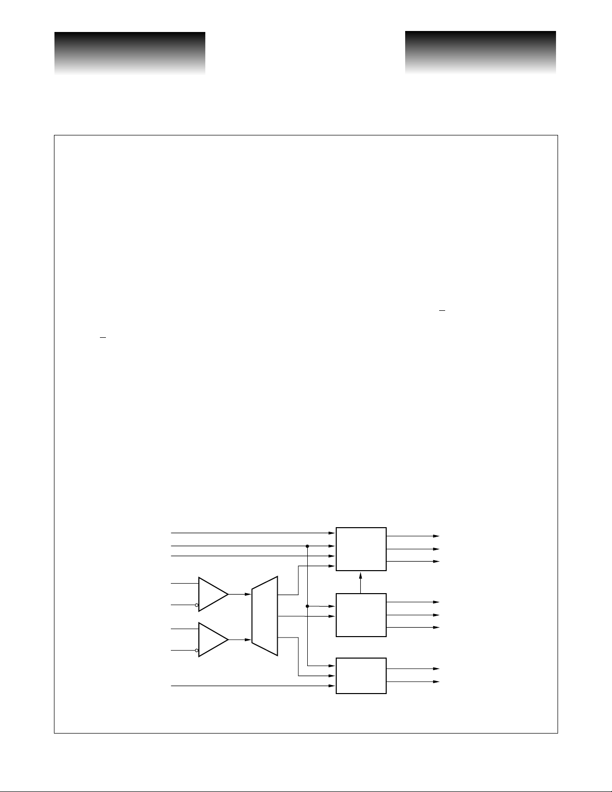
General Description
The VSC8132 demultiplexes a 2.488Gb/s HSPECL serial input datastre am (DI+) to 32-bit wide, TTL
77.76Mb/s parallel data outputs D[31:0] for SONET/SDH applications . A 2.488GHz HSPECL input clock
(CLKI+
and 38.88MHz, are generated for upst ream d evi ces ( DATACLK78, CLK51, C LK38 ). Odd or ev en pa r ity i s per formed on the incoming high-speed data via the TTL Parity Select input (PARSEL), and a TTL Parity output
(PARITY) is provided to indicate parity of the input data. Frame Detect on the incoming data is controlled via
the Frame Detect Inhibit (OOFN) and Reset (RESET) TTL inputs. A frame detect monitors the incoming data
steam and screens for 2 bits in A1 byte out of the 8 bits and 2 bits of A2 byte out of the 8 bits. When a Frame
Detect occurs, a synchronization TTL output (SYNC) will be set. Alarm indicators are used to monitor the
activity of the clock and data with TTL compatible control inputs (ALMRESET) and outputs (DTALARM,
CKALARM).
mally-enhanced 128-pin, 14x20x2mm PQFP package.
) is used to time the incoming data and 3 TTL clock outputs, at frequencies of 77.76MHz, 51.84MHz,
Only a single 3.3V power supply is required for device operation. The VSC8132 is packaged in a ther-
VSC8132 Block DIagram
OOFN
RESET
PARSEL
DI+
DI–
CLKI+
CLKI–
ALMRESET
G52250-0, Rev 3.1 Page 1
12/7/00
© VITESSE SEMICONDUCTOR CORPORATION • 741 Calle Plano • Camarillo, CA 93012
Tel: (800) VITESSE • FAX: (805) 987-5896 • Email: prodinfo@vitesse.com
1:32
Demux
Internet: www.vitesse.com
Framing
and
Parity
Clock
Generation
Alarms
DATA[3:0]
SYNC
PARITY
DATACLK78
CLK51
CLK38
DTALARM
CKALARM
Page 2
VITESSE
SEMICONDUCTOR CORPORATION
Preliminary Data Sheet
2.488Gb/s 1:32 SONET/SDH Demux
VSC8132
Functional Description
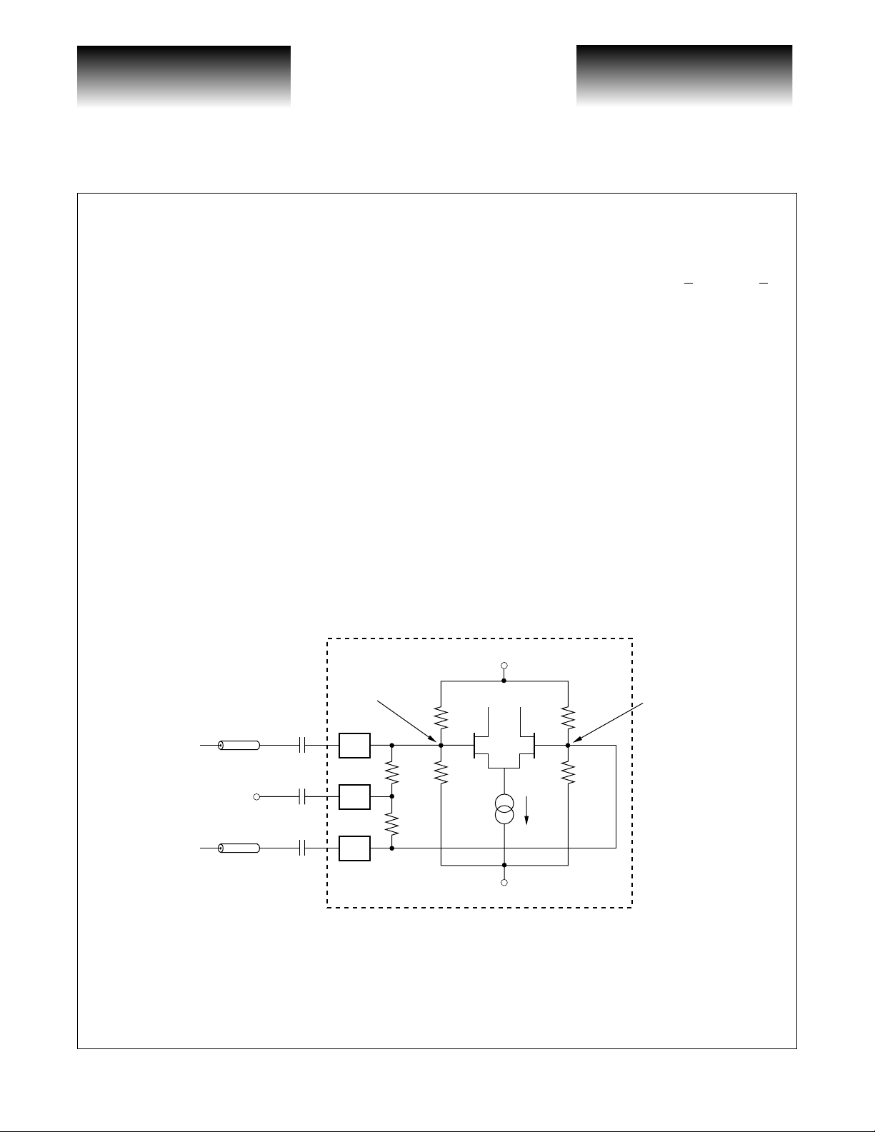
High-Speed Clock and Data Interface
The incoming high-speed data and high-speed clock are received by high-speed inputs DI+ and CLKI+.
The inputs are internally biased to accommodate AC-coupling.
The data and clock inputs are internally terminated by a center-tapped resistor network. For differential
input DC-couplin g, the network is terminated to the appropriate termination voltage,
V
termination for both true and complement inputs. For differential input AC-coupling, the network is ter-
TERM
minated to
V
via a blocking capacitor.
TERM
In most situations, these inputs will have high transition density and little DC offset. However, in cases
where this does not hold, direct DC connection i s possible . All serial data and clock in puts have t he same circuit
topology as shown in Figure 1. The reference voltage is created by a resistor divider as shown. If the input signal is driven differentially and DC-coupled to the part, the mid-point of the input signal swing should be centered about this reference voltage and not exceed the maximum allowable amplitude. For single-ended, DCcoupling operations, it is recommended th at the user provides an externa l reference voltage whic h has better
temperature and power supply noise rejection than the on-chip resistor divider. The external reference should
have a nominal value equivalent to the common mode switch point of the DC-coupled signal, and can be connected to either side of th e differential gate.
Figure 1: High-Speed Clock and Data Inputs
V
providing a 50 Ω to
TERM
V
Z
TERM
Z
Chip Boundary
V
= 3.3V
CC
C
IN
0
0
100nF
C
AC
100nF
C
IN
100nF
1.65V
50Ω
50Ω
3kΩ
3kΩ
3kΩ
3kΩ
I
I
= 0V
V
EE
1.65V
Page 2 G52250-0, Rev 3.1
© VITESSE SEMICONDUCTOR CORPORATION • 741 Calle Plano • Camarillo, CA 93012
Tel: (800) VITESSE • FAX: (805) 987-5896 • Email: prodinfo@vitesse.com
Internet: www.vitesse.com
12/7/00
Page 3

Preliminary Data Sheet
VITESSE
SEMICONDUCTOR CORPORATION
VSC8132
Low-Speed Data Interface
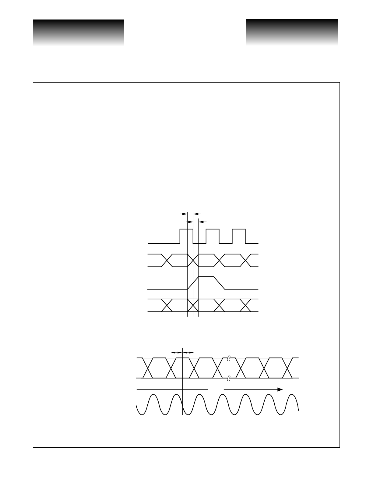
The 77.76Mb/s parallel data outputs D[31:0] are clocked out of the VSC8132 on the falling clock edge of
the 77.76MHz output clock (DATA78CLK). The data and clock are TTL levels. The MSB (D31) bit is the first
bit into the serial interface.
Parity Selection
The parity output bit (PARITY) is clocked out on the falling edge of the 77.76MHz clock (DATA78CLK).
This bit indicates the parity of the 32 bits of data along with the frame sync bit. The parity of the output is determined by the parity select in put ( PARSEL). When t he parit y select in put is L OW, the outp ut pari ty is od d. When
the parity select is HIGH, the output parity is even. The parity inputs and outputs are TTL levels. See Figure 2
for output timing relationship.
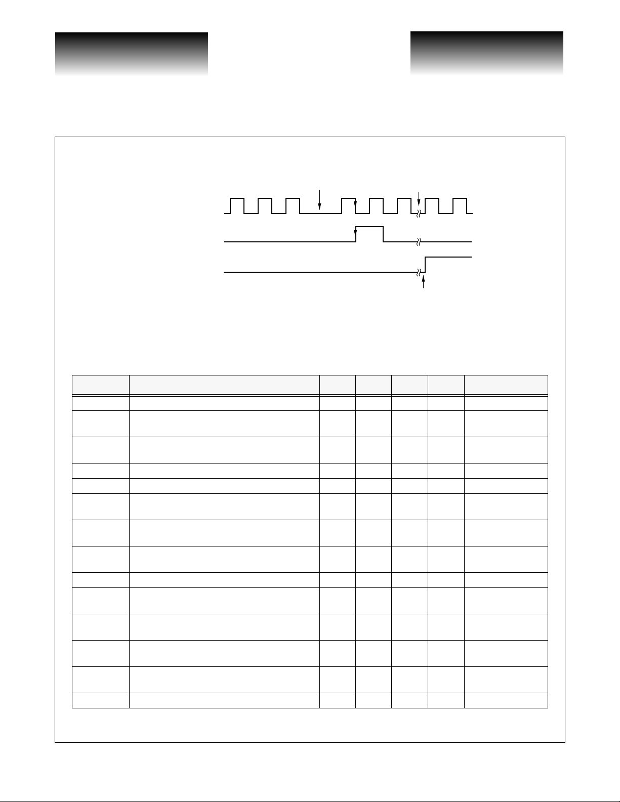
Framing Logic Interface
When a frame detect occurs and t he f ra me d ete ct i nh ib it input ( OOFN) i s set L OW, the frame det ect output
(SYNC) is set HIGH on the negative edge of the 77.76MHz clock and on the 3rd set of four A2 bytes at the 32bit data output. The frame detect mechanism is inhibited when the frame detect inhibit (OOFN) input is set
HIGH. The frame detect output and frame detect inhibit are TTL levels.
NOTE: The 77.76MHz clock miss es one clock cycle during a frame detect. This m issed cycle oc curs one
clock period before the Sync pulse is set HIGH (see Figure 4).
To use as a framer:
Step 1: Set OOFN LOW
Step 2:Wait for Sync pulse
Step 3:When Sync Pulse goes HIGH, set OOFN HIGH
2.488Gb/s 1:32 SONET/SDH Demux
Chip Reset
Chip reset (RESET) will reset the framing logic so that no fram e detection barrel shift ing is performed.
Therefore, if the fra me d ete ct inh ibit inp ut is set h igh , the ch ip w ill ac t as a sim ple de mux afte r re set. T he reset
should be set high for 16 clock cycles of the high speed clock input. The chip reset is a TTL level.
Alarm Logic Interface
The Loss of Clock (CKALARM) and Loss of Data (DTALARM) alarms monitor the activity of the clock
and data. The Alarm Reset (ALMRESET) input controls the alarm activity . Polling of the alarms signals are initiated by toggling the Alar m Reset in put HIGH and the n LOW on e ti me. To reset both alarm output s, th e Alar m
Reset should be toggled HIGH to LOW two times. All alarm logic interface signals are TTL levels.
Supplies
The VSC8132 is specified as a HSPECL/TTL device with a single positive 3.3V supply. Normal operation
is to have V
a negative 3.3V supply, V
put signals are still referenced to V
G52250-0, Rev 3.1 Page 3
12/7/00
= +3.3V and V
CC
© VITESSE SEMICONDUCTOR CORPORATION • 741 Calle Plano • Camarillo, CA 93012
= ground. Should the user desire to use the device in a ECL environment with
EE
will be ground and VEE will be -3.3V. If used with VEE tied to -3.3V, the TTL out-
CC
.
EE
Tel: (800) VITESSE • FAX: (805) 987-5896 • Email: prodinfo@vitesse.com
Internet: www.vitesse.com
Page 4
VITESSE
SEMICONDUCTOR CORPORATION
Preliminary Data Sheet
2.488Gb/s 1:32 SONET/SDH Demux
Decoupling of the power supplies is a critical element in maintaining the proper operation of the part. It is
recommended that the V
on each V
power supply pin as close to the package as possible. If room permits, a 0.001µF capacitor should
CC
also be placed in parallel with the 0.1
low-inductance ceramic SMT X7R devices. For the 0.1
0.01
µF and 0.001µF capacitors can be either 0603 or 0402 packages.
For low frequency decoupling, 47
power supply be decoupled using a 0.1µF and 0.01µF capacitor placed in parallel
CC
µF and 0.01µF capacitors mentioned above. Recommended capacitors are
µF capacitor, a 0603 package should be used. The
µF tantalum, low-inductance SMT caps should be sprink led over the
board’s main +3.3V power supply and placed close to the C-L-C pi filter.
If the device is being used in an ECL environment w ith a -3.3V supply, all references to decoupling V
must be changed to VEE, and all references to decoupling 3.3V must be changed to -3.3V.
AC Characteristics
Figure 2: Output Timing
t
PD1
t
PD2
78MHz CLK
VSC8132
CC
78MHz DATA
SYNC PULSE
PARITY
DI+
Differential Serial Data Input
CLKI+
Differential Clock Input
Figure 3: Data Output Timing
t
SERSU
D31 D0
MSB
NOTE: Bit 31 (MSB) is received first, Bit 0 (LSB) is received last.
t
SERHO
Time
LSB
Page 4 G52250-0, Rev 3.1
© VITESSE SEMICONDUCTOR CORPORATION • 741 Calle Plano • Camarillo, CA 93012
Tel: (800) VITESSE • FAX: (805) 987-5896 • Email: prodinfo@vitesse.com
Internet: www.vitesse.com
12/7/00
Page 5
Preliminary Data Sheet
VITESSE
SEMICONDUCTOR CORPORATION
VSC8132
2.488Gb/s 1:32 SONET/SDH Demux
Figure 4: Framing Sequence
Missed Clock
(1)
Pulse
OOFN (In)
(1)
(asynchronous)
CLK78 (Out)
SYNC PULSE (Out)
NOTE: (1) No missing clock pulse for CLK78 when VSC8132 is working as a dumb demux.
Once frame occurs and OOFN is set HIGH, the no framing will occur until
OOFN is set LOW again. The VSC8132 will remain framed with SONET frame.
Approximately <110µs
Set HIGH, less than 110µs
after SYNC goes HIGH
T a ble 1: AC Characteristics
Parameters Description Min Typ Max Units Conditions
t
DATApd
t
CLKRpd
t
CLKFpd
t
DEDGE
t
CLKEDGE
t
CONEDGE
t
SERSU
t
SERHO
f
MAX
t
CLK38Rpd
t
CLK38Fpd
t
CLK51Rpd
t
CLK51Fpd
, t
t
PD1
PD2
Data Valid From Falling Edge of 77.76MHz 230 1250 ps External load = 5pf
High-speed Clock Rising Edge to 77.76M Hz
Clock Rising Edge
High-Speed Cl oc k R i si ng E dg e to 77 .7 6MHz
Clock Fallin g Edge
2.5 8.0 ns External load = 5pf
2.3 7.1 ns External load = 5pf
D[0:31] Edge Rate (10%-90%) - 2.0 ns External load = 5pf
77.76, 51.84, 38.88MHz Edge Rates (10%-90%) - 2.0 ns External load = 5pf
Control Signals (SYNC, PARITY, DTALARM,
and CKALARM) Edge Rate (10%-90%)
DI+ Setup Time with Respect to Falling Edg e of
CLKI+
DI+ Hold Time with Respect to Falling Edge of
CLKI+
-2.0ns
100 - ps See Figure 3
75 - ps See Figure 3
External load = 5pf
Demux Input Maximum Clock Frequency - 2.9 GHz
High-Speed Cl oc k R i si ng E dg e to 38 .8 8MHz
Clock Rising Edge.
High-Speed Cl oc k R i si ng E dg e to 38 .8 8MHz
Clock Fallin g Edge
High-Speed Cl oc k R i si ng E dg e to 51 .8 4MHz
Clock Rising Edge
High-Speed Cl oc k R i si ng E dg e to 51 .8 4MHz
Clock Fallin g Edge
2.0 6.3 ns External load = 5pf
2.0 5.9 ns External load = 5pf
2.0 6.0 ns External load = 5pf
2.0 5.9 ns External load = 5pf
Data Invalid Window 0, 230 0, 1250 ps
G52250-0, Rev 3.1 Page 5
12/7/00
© VITESSE SEMICONDUCTOR CORPORATION • 741 Calle Plano • Camarillo, CA 93012
Tel: (800) VITESSE • FAX: (805) 987-5896 • Email: prodinfo@vitesse.com
Internet: www.vitesse.com
Page 6

VITESSE
SEMICONDUCTOR CORPORATION
Preliminary Data Sheet
2.488Gb/s 1:32 SONET/SDH Demux
DC Characteristics
T a ble 2: DC Characteristics (Over recommended operating conditions)
Parameters Description Min Typ Max Units Conditions
V
OHttl
V
OLttl
V
IHttl
V
ILttl
V
OHpecl
V
OLpecl
∆V
DIFF(CLKI)
∆V
DIFF(DI)
V
CC
P
D
I
DD
Output HIGH Voltage (TTL) 2.4 ——VIOH = -1.0mA
Output LOW Voltage (TTL) ——0.5 V IOL = +1.0mA
Input HIGH Voltage (TTL) 2.0 ——VIIH = 300µA
Input LOW Voltage (TTL) ——0.8 V IIL = -50µA
-
V
Output HIGH Voltage (HSPECL)
Output LOW Voltage (HSPECL)
Demux Clock Input Absolute Voltage
Differential Peak-to-Peak Swing
)
(CLKI+
Demux Serial Input Absolute Voltage
Differential Peak-to-Peak Swing (DI+
Supply Voltage 3.14 — 3.47 V 3.3V± +5%
Power Dissipation — 1.6 2.05 W Outputs open, VCC = VCC max
Supply Current — 489 591 mA Outputs open, VCC = VCC max
CC
1.02
VCC-
2.0
400
400
)
—
—
—
—
-
V
CC
0.7
VCC-
1.62
1200 mV
1200 mV
V Output tied to 50Ω to V
V Output tied to 50Ω to VCC-2.0V
AC-coupled, internally biased
/2
to V
CC
AC-coupled, internally biased
to VCC/2
VSC8132
-2.0V
CC
Absolute Maximum Ratings
(1)
Power Supply Voltage (VCC)...........................................................................................................-0.5V to +3.8V
DC Input Voltage (differential inputs).....................................................................................-0.5V to V
CC
+0.5V
Output Current (differential outputs)...........................................................................................................±50mA
Case Temperature Under Bias......................................................................................................-55
Storage Temperature.....................................................................................................................-65
o
C to +125oC
o
C to +150oC
Maximum Input ESD (Human Body Model)............................................................................................... 1500V
NOTE: (1) CAUTION: Stresses listed under “Absolute Maximum Ratings” may be applied to devices one at a time without caus-
ing permanent damage. Functionality at or above the values listed is not implied. Exposure to these values for extended
periods may affect device reliability.
Recommended Operating Conditions
Power Supply Voltage (VCC).................................................................................................................+3.3V+5%
Operating Temperature Range .............................................................0
Figure 5: Parametric Measurement Information
TTL Rise and Fall Time
t
R
o
C Ambient to +85oC Case Temperat ure
90%
10%
t
F
Page 6 G52250-0, Rev 3.1
© VITESSE SEMICONDUCTOR CORPORATION • 741 Calle Plano • Camarillo, CA 93012
Tel: (800) VITESSE • FAX: (805) 987-5896 • Email: prodinfo@vitesse.com
Internet: www.vitesse.com
12/7/00
Page 7

Preliminary Data Sheet
VITESSE
SEMICONDUCTOR CORPORATION
VSC8132
Package Pin Descriptions
VCC
VEE
VEE
128
127
126
NC
NC
NC
VCC
NC
VEECTERM
NC
VCC
CLKI+
CLKI-
NC
VEE
DI+
DI-
VEEDTERM
VEE
VEE
NC
NC
NC
VCC
NC
VCC
VCC
VCC
VEE
VEE
VEE
VEE
VEE
NC
NC
NC
RESET
NC
NC
NC
NC
1
2
3
4
5
6
7
8
9
10
11
12
13
14
15
16
17
18
19
20
21
22
23
24
25
26
27
28
29
30
31
32
33
34
35
36
37
38
THTRIST6
DTALARM
VCC
125
124
123
Figure 6: Pin Diagram
VEE
ALMRESET
THRIST4
VEE
VCC
THRIST1
PARSEL
THRIST5
THPAR
122
121
120
119
118
117
116
115
114
VCC
113
SYNC
112
2.488Gb/s 1:32 SONET/SDH Demux
DATACLK78
VEE
TH78DT0 (LSB)
TH78DT1
VCC
TH78DT2
TH78DT3NCVCC
111
110
109
108
107
106
105
104
103
VCC
102
TH78DT4
101
TH78DT5
100
VCC
99
TH78DT6
98
TH78DT7
97
VEE
96
TH78DT8
95
TH78DT9
94
VCC
93
TH78DT10
92
TH78DT11
91
VCC
90
TH78DT12
89
TH78DT13
88
VEE
87
VSC8132
VITESSE
TH78DT14
86
TH78DT15
85
VCC
84
TH78DT16
83
TH78DT17
82
VCC
81
TH78DT18
80
TH78DT19
79
VEE
78
TH78DT20
77
TH78DT21
76
VCC
75
TH78DT22
74
TH78DT23
73
VCC
72
TH78DT24
71
TH78DT25
70
VEE
69
TH78DT26
68
TH78DT27
67
VCC
66
NC
65
39404142434445464748495051525354555657585960616263
VEE
VCC
NCNCNC
OOFN
VEE
CLK51-
CLK51+
VCC
CLK38-
CLK38+
VCC
THTRIST2
Internet: www.vitesse.com
VEE
THTRIST3
TH78DT31 (MSB)
VCC
TH78DT30
VEE
VCC
CKALARM
G52250-0, Rev 3.1 Page 7
12/7/00
© VITESSE SEMICONDUCTOR CORPORATION • 741 Calle Plano • Camarillo, CA 93012
Tel: (800) VITESSE • FAX: (805) 987-5896 • Email: prodinfo@vitesse.com
NC
TH78DT29
TH78DT28
64
VCC
Page 8

VITESSE
SEMICONDUCTOR CORPORATION
Preliminary Data Sheet
2.488Gb/s 1:32 SONET/SDH Demux
Table 3: Pin Identifications
Pin Name I/O Level Description
1 NC - - No Connect, Leave Unconnected
2
3
4
5
6
7
8
9
10
11
12
13
14
15
16
17
18
19
20
21
22
23
24
25
26
27
28
29
30
31
32
33
34
NC - - No Connect, Leave Unconnected
NC - - No Connect, Leave Unconnected
VCC - +3.3V Power Supply
NC - - No Connect, Leave Unconnected
VEECTERM - GND 50Ω Termination Ground for CLK±
NC - - No Connect, Leave Unconnected
VCC - +3.3V Power Supply
CLKI+ I HSPECL High-Speed Clock Input, True
CLKI- I HSPECL High-Speed clock Input, Complement
NC - - No Connect, Leave Unconnected
VEE - 0V Ground
DI+ I HSPECL
DI- I HSPECL
VEEDTERM - GND 50Ω Termination Ground for DI±
VEE - 0V Ground
VEE - 0V Ground
NC - - No Connect, Leave Unconnected
NC - - No Connect, Leave Unconnected
NC - - No Connect, Leave Unconnected
VCC - +3.3V Power Supply
NC - - No Connect, Leave Unconnected
VCC - +3.3V Power Supply
VCC - +3.3V Power Supply
VCC - +3.3V Power Supply
VEE - 0V Ground
VEE - 0V Ground
VEE - 0V Ground
VEE - 0V Ground
VEE - 0V Ground
NC - - No Connect, Leave Unconnected
NC - - No Connect, Leave Unconnected
NC - - No Connect, Leave Unconnected
RESET I/O TTL Resets Framing Logic and Output Clocks
VSC8132
High-Speed Ser ial Data Input, True. PECL l evels, AC-couple d,
internally biased to V
High-Speed Serial Data Input, Complement. PECL levels, ACcoupled, internally biased to V
CC
/2.
CC
/2.
Page 8 G52250-0, Rev 3.1
© VITESSE SEMICONDUCTOR CORPORATION • 741 Calle Plano • Camarillo, CA 93012
Tel: (800) VITESSE • FAX: (805) 987-5896 • Email: prodinfo@vitesse.com
Internet: www.vitesse.com
12/7/00
Page 9

Preliminary Data Sheet
VITESSE
SEMICONDUCTOR CORPORATION
VSC8132
Pin Name I/O Level Description
35
36
37
38
39
40
41
42
43
44
45
46
47
48
49
50
51
52
53
54
55
56
57
58
59
60
61
62
63
64
65
66
67
68
2.488Gb/s 1:32 SONET/SDH Demux
NC - - No Connect, Leave Unconnected
NC - - No Connect, Leave Unconnected
NC - - No Connect, Leave Unconnected
NC - - No Connect, Leave Unconnected
VCC - +3.3V Power Supply
VEE - 0V Ground
CKALARM O TTL Loss of clock output. Sta y s H IG H whe n loss of clo c k i s dete c te d.
VEE - 0V Ground
VCC - +3.3V Power Supply
OOFN I TTL
NC - - No Connect, Leave Unconnected
NC - - No Connect, Leave Unconnected
NC - - NNo Connect, Leave Unconnected
CLK51- O HSPECL L ow-Speed Clock Output (51.84MHz), Complement
CLK51+ O HSPECL Low- Speed Clock Output (51.84MHz), True
VCC - +3.3V Power Supply
VEE - 0V Ground
CLK38- O HSPECL L ow-Speed Clock Output (38.88MHz), Complement
CLK38+ O HSPECL Low speed Clock Output (38 .88MHz), True
VCC - +3.3V Power Supply
THTRIST2 I TTL
THTRIST3 I TTL
VEE - 0V Ground
TH78DT31 O TTL Low-Speed Parallel Data (MSB)
TH78DT30 O TTL Low-Speed Parallel Data
VCC - +3.3V Power Supply
TH78DT29 O TTL Low-Speed Parallel dData
TH78DT28 O TTL Low-Speed Parallel Data
NC - - No connect, leave uncon nected
VCC - +3.3V Power Supply
NC - - No Connect, Leave Unconnected
VCC - +3.3V Power Supply
TH78DT27 O TTL Low-Speed Parallel Data
TH78DT26 O TTL Low-Speed Parallel Data
Frame Detect Disable Input. Disables frame detection if set
HIGH.
Tri-State Inputs. Allows tri-sta ting o f all o utput signals. Used for
test only. Should be tied to VEE during normal ope r at ion.
Tri-State Inputs. Allows tri-sta ting o f all o utput signals. Used for
test only. Should be tied to V
during normal ope r at ion.
EE
G52250-0, Rev 3.1 Page 9
12/7/00
© VITESSE SEMICONDUCTOR CORPORATION • 741 Calle Plano • Camarillo, CA 93012
Tel: (800) VITESSE • FAX: (805) 987-5896 • Email: prodinfo@vitesse.com
Internet: www.vitesse.com
Page 10

VITESSE
SEMICONDUCTOR CORPORATION
Preliminary Data Sheet
2.488Gb/s 1:32 SONET/SDH Demux
Pin Name I/O Level Description
69
70
71
72
73
74
75
76
77
78
79
80
81
82
83
84
85
86
87
88
89
90
91
92
93
94
95
96
97
98
99
100
101
102
103
104
VEE - 0V Ground
TH78DT25 O TTL Low-Speed Parallel Data
TH78DT24 O TTL Low-Speed parallel Data
VCC - +3.3V Power Supply
TH78DT23 O TTL Low-Speed Parallel Data
TH78DT22 O TTL Low-Speed Parallel Data
VCC - +3.3V Power Supply
TH78DT21 O TTL Low-Speed Parallel Data
TH78DT20 O TTL Low-Speed Parallel Data
VEE - 0V Ground
TH78DT19 O TTL Low-Speed Parallel Data
TH78DT18 O TTL Low-Speed Parallel Data
VCC - +3.3V Power Supply
TH78DT17 O TTL Low-Speed Parallel Data
TH78DT16 O TTL Low-Speed Parallel Data
VCC - +3.3V Power Supply
TH78DT15 O TTL Low-Speed Parallel Data
TH78DT14 O TTL Low-Speed Parallel Data
VEE - 0V Ground
TH78DT13 O TTL Low-Speed Parallel Data
TH78DT12 O TTL Low-Speed Parallel Data
VCC - +3.3V Power Supply
TH78DT11 O TTL Low-Speed Parallel Data
TH78DT10 O TTL Low-Speed Parallel Data
VCC - +3.3V Power Supply
TH78DT9 O TTL Low-Speed Parallel Data
TH78DT8 O TTL Low-Speed Parallel Data
VEE - 0V Ground
TH78DT7 O TTL Low-Speed Parallel Data
TH78DT6 O TTL Low-Speed Parallel Data
VCC - +3.3V Power Supply
TH78DT5 O TTL Low-Speed Parallel Data
TH78DT4 O TTL Low-Speed Parallel Data
VCC - +3.3V Power Supply
VCC - +3.3V Power Supply
NC - - No Connect, Leave Unconnected
VSC8132
Page 10 G52250-0, Rev 3.1
© VITESSE SEMICONDUCTOR CORPORATION • 741 Calle Plano • Camarillo, CA 93012
Tel: (800) VITESSE • FAX: (805) 987-5896 • Email: prodinfo@vitesse.com
Internet: www.vitesse.com
12/7/00
Page 11

Preliminary Data Sheet
VITESSE
SEMICONDUCTOR CORPORATION
VSC8132
Pin Name I/O Level Description
105
106
107
108
109
110
111
112
113
114
115
116
117
118
119
120
121
122
123
124
125
126
127
128
2.488Gb/s 1:32 SONET/SDH Demux
TH78DT3 O TTL Low-Speed Parallel Data
TH78DT2 O TTL Low-Speed Parallel Data
VCC - +3.3V Power Supply
TH78DT1 O TTL Low-Speed Parallel Data
TH78DT0 O TTL Low-Speed Parallel Data (LSB)
VEE - 0V Ground
DATACLK78 O TTL
SYNC O TTL Frame Detect Output. Set HIGH when frame detect occurs.
VCC - +3.3V Power Supply
THPAR O TTL Parity Output
THTRIST5 I TTL
PARSEL I TTL Parity Select Input. HIGH for even; LOW for odd.
THTRIST1 I TTL
VCC - +3.3V Power Supply
VEE - 0V Ground
THTRIST4 I TTL
ALMRESET I TTL
VEE - 0V Ground
VCC - +3.3V Power Supply
DTALARM O TTL Loss of Data Output. Stays HIGH when loss of data is detected.
THTRIST6 I TTL
VEE - 0V Ground
VEE - 0V Ground
VCC - +3.3V Power Supply
Low-Speed Clock Out put (77.76MHz). A div ide-by-32 versio n
of the CLKI±
Tri-State Inputs. Allows tri-sta ting o f all o utput signals. Used for
test only. Should be tied to V
Tri-State Inputs. Allow tri-stating of all output signals. Used for
test only. Should be tied to V
Tri-State Inputs. Allow tri-stating of all output signals. Used for
test only. Should be tied to V
Alarm Reset. Resets and clocks out Loss of Clock and Loss of
Data alarm s .
Tri-state Inputs. Allow tri-stating of all output signals. Used for
test only. Should be tied to V
input clock.
during normal ope r at ion.
EE
during normal ope r at ion.
EE
during normal ope r at ion.
EE
during normal ope r at ion.
EE
G52250-0, Rev 3.1 Page 11
12/7/00
© VITESSE SEMICONDUCTOR CORPORATION • 741 Calle Plano • Camarillo, CA 93012
Tel: (800) VITESSE • FAX: (805) 987-5896 • Email: prodinfo@vitesse.com
Internet: www.vitesse.com
Page 12

VITESSE
SEMICONDUCTOR CORPORATION
Preliminary Data Sheet
2.488Gb/s 1:32 SONET/SDH Demux
Package Information
PIN 128
PIN 1
RAD. 2.92 ± .50
(2)
EXPOSED
HEATSINK
EXPOSED
INTRUSION
0.127 MAX.
D
D
TOP VIEW
10° TYP .
128-Pin PQFP Package Drawing
E
E
1
2.54 ± .50
1
VSC8132
Key mm Tolerance
A2.35 MAX
A1 0.25 MAX
A2 2.00 +.10
D 17.20 ±.20
D1 14.00 ±.10
E 23.20 ±.20
E1 20.00 ±.10
L .88 +.15/-.10
e.50BASIC
b .22 ±.05
θ 0°-7°
R.30 TYP
R1 .20 TYP
A
2
A
1
10° TYP .
R
R1
θ
1
.25
A
Notes: 1) Drawing is not to scale
2) All dimensions in mm
3) Package represented is
also used for the 64,
80, & 100 PQFP packages.
Pin count drawn does
not reflect the 128 Package.
Page 12 G52250-0, Rev 3.1
© VITESSE SEMICONDUCTOR CORPORATION • 741 Calle Plano • Camarillo, CA 93012
Tel: (800) VITESSE • FAX: (805) 987-5896 • Email: prodinfo@vitesse.com
0.17
θ
MAX.
L
Internet: www.vitesse.com
e
b
A
STANDOFF
A
1
LEAD COPLANARITY
NOTES:
Package #: 101-267-7
Issue #: 1
12/7/00
Page 13

Preliminary Data Sheet
VITESSE
SEMICONDUCTOR CORPORATION
VSC8132
2.488Gb/s 1:32 SONET/SDH Demux
Package Thermal Considerations
The VSC8132 has been enhanced with a copper heat slug to provide a low thermal resistance path from the
die to the exposed surface of the heat spreader. The thermal resistance is shown in Table 4.
T a ble 4: Thermal Resistance
Symbol Description °C/W
θ
JC
θ
JA
Thermal Resistance with Airflow
Thermal resistanc e wit h airflow is s hown i n Table 5. The thermal resistan ce val ue re flects all the therma l
paths including through the leads in an environment where the leads are exposed. The temperature difference
between the ambient airflow temperature and the case temperature should be t he worst-case power of the devi ce
multiplied by the thermal resistance.
T a ble 5: Thermal Resistance with Airflow
Airflow θCA (
100 lfpm 19.8
200 lfpm 16.7
400 lfpm 14.6
600 lfpm 13.0
Thermal resistance from junction-to-case. 2.2
Thermal resistance from junction-to -amb ie nt with no airflow, including
conduction through the leads.
o
C/W)
26.8
Maximum Ambient Temperature without Heatsink
The worst case ambient temperature without use of a heatsink is given by the equation:
T
AMAX()TCMAX()
=
P–
MAX()
θ
CA
where:
T
A(MAX)
Τ
C(MAX)
P
(MAX)
θ
CA
G52250-0, Rev 3.1 Page 13
12/7/00
Ambient air temperature
Case temperature (+85oC)
Power (2.05W)
Theta case-to-ambient at appropriate airflow
© VITESSE SEMICONDUCTOR CORPORATION • 741 Calle Plano • Camarillo, CA 93012
Tel: (800) VITESSE • FAX: (805) 987-5896 • Email: prodinfo@vitesse.com
Internet: www.vitesse.com
Page 14

VITESSE
SEMICONDUCTOR CORPORATION
Preliminary Data Sheet
2.488Gb/s 1:32 SONET/SDH Demux
The results of this calculation are listed in Table 6.
Table 6: Maximum Ambient Air Temperature without Heatsink
Airflow
None 35.6
100 lfpm 44.4
200 lfpm 50.8
400 lfpm 55.1
600 lfpm 58.4
Note that ambient air temperature varies throughout the system based on the positioning and magnitude of
heat sources and the direction of air flow.
Max Ambient Temperature
o
C)
(
Ordering Informatio n
The order number for this product is formed by a combination of the device type and package type
VSC8132
VSC8132
xx
Device Type
2.488Gb/s 1:32 Demux, 3.3V
Package
QR: 128-Pin PQFP, 14x20x2mm Body
Notice
Vitesse Semiconductor Corporation (“Vitesse”) pr ovides th is docum ent for inform ational purposes o nly. This document conta ins
pre-production information about Vitesse products in their concept, development and/or testing phase. All information in this document, including descriptions of features, functions, performance, technical specifications and availabiity, is subject to change
without notice at any time. Nothing contained in this document shall be construed as extending any warranty or promise, express
or implied, that any Vitesse product will be available as described or will be suitable for or will accomplish any particular task.
Warning
Vite sse S emic o nduc to r Co rpo ra tion’s products are not intended for use in life support ap plia nc es, de vi ces o r syste ms. Use of a Vit-
esse product in such applications without written consent is prohibited.
Page 14 G52250-0, Rev 3.1
© VITESSE SEMICONDUCTOR CORPORATION • 741 Calle Plano • Camarillo, CA 93012
Tel: (800) VITESSE • FAX: (805) 987-5896 • Email: prodinfo@vitesse.com
Internet: www.vitesse.com
12/7/00
 Loading...