

Page 1

VITESSE
SEMICONDUCTOR CORPORATION
Data Sheet
VSC8122
Multi-Rate SONET/SDH
Clock and Data Recovery IC
Features
• Multi-Rate OC-3, OC-12, OC-24, OC-48 Clock
and Data Recovery
• Supports Gigabit Ethernet
• Differential Back Terminated I/O
• Maintains Clock Output in the Absence of Data
• Selectable Reference Clock
• Loss of Lock Indicator
• Exceeds SONET/SDH Requirements for Jitter
Tolerance, Jitter Transfer and Jitter Generati on.
• 3.3V Supply Ope r ation
• 1W Typical Power
• 64-pin , 10x10mm PQFP Packaging
General Description
The VSC8122 is a single-chip clock recovery IC for use in SONET OC-48, OC-24, OC-12, OC-3, or Giga-
bit Ethernet systems operating at their respective 2.48832Gb/s, 1.24416Gb/s, 622.08Mbps, 155.52Mbps, or
1.25Gbps data rates. The VSC8122 complies with SONET jitter tolerance, jitter transfer and jitter generation
specifications.
Alarm functions support typical telecom system applications. The Loss of Lock (LOL) output indicates
when the devic e goes out of lock, which wo uld most of ten occu r in the e v ent of a loss of v ali d dat a. The NOREF
output flags when the reference input to the VSC8122 either is removed, or goes severely out of tolerance.
VSC8122 Block Diagram
DI+
DI-
REFCK1 +/REFCK0 +/-
Ph/Freq.
Detector
REF_INPUTSEL
FILTO+/-
Divider
FILTI+/-
Loop
Filter
REF_SEL[1:0]
VCO
FSEL[1:0]
Divider
Data
Retiming
Lock
Detect
CO+
CO-
DO+
DO-
LOL
NOREF
G52228-0, Rev 4.1 Page 1
01/05/01
© VITESSE SEMICONDUCTOR CORPORATION • 741 Calle Plano • Camarillo, CA 93012
Tel: (800) VITESSE • FAX: (805) 987-5896 • Email: prodinfo@vitesse.com
Internet: www.vitesse.com
Page 2
VITESSE
SEMICONDUCTOR CORPORATION
Multi-Rate SONET/SDH
Clock and Data Recovery IC
Data Sheet
VSC8122
Functional Description
Data Input
The data input receiver is internally terminated by a center-tapped resistor network. For differential input
AC coupling, the network is terminated to the appropriate termination voltage, V
capacitor, C
to ground. The input requires a differential signal with a peak-to-peak voltage on both the true
AC
and complement of a minimum of 250mV. These inputs are required to be AC-coupled to allow use with a variety of limiting amplifiers.
Figure 1: Input Termination (AC-Coupled)
VSC8122Limiting Amp
Zo = 50Ω
0.1 µF
C
AC
DI+
50Ω
V
50Ω
TERM
through a blocking
TERM
Z
= 50Ω
o
0.1 µF
DI-
High-Speed Clock and Data Outputs
The VSC8122 high-speed clock and data outputs can be DC-terminated, 50 Ω to VCC as indicated in
Figure 2.
Figure 2: High-Speed Clock and Data Output DC Termination
VSC8122
V
CC
50Ω
50Ω
V
CC
CO+ / DO+
CO- / DO-
100Ω
100Ω
V
CC
Zo = 50Ω
= 50Ω
Z
o
V
CC
Page 2 G52228-0, Rev 4.1
© VITESSE SEMICONDUCTOR CORPORATION • 741 Ca l le Pl an o • Camarillo, CA 93012
Tel: (800) VITESSE • FAX: (805) 987-5896 • Email: prodinfo@vitesse.com
Internet: www.vitesse.com
01/05/01
Page 3

VITESSE
SEMICONDUCTOR CORPORATION
Data Sheet
VSC8122
Outputs can also be A C t erminated as sho wn in Figure 3 . The ou tput differential voltag e and common-mode
voltage range are specified in Table 4, High-Speed Inputs and Outputs.
Figure 3: High-Speed Clock and Data Output AC Termination
VSC8122
V
CC
100Ω
CO+ / DO+
CO- / DO-
Clock Recovery
100Ω
V
CC
The VSC8122 has a selectable input data rate. Two pins (FSEL0 and FSEL1) select the data rate to be provided to the VSC8122.
0.1µF
0.1µF
Zo = 50Ω
= 50Ω
Z
o
Multi-Rate SONET/SDH
Clock and Data Recovery IC
V
TERM
50Ω
50Ω
V
TERM
Table 1: Input Data Rate Select
Input Data Rate FSEL0 FSEL1
2.48832Gb/s or 2.5Gb/s
1.24416Gb/s or 1.25Gb/s
622.08Mb/s or 625Mb/s
155.52Mb/s or 156.25Mb/s
00
10
01
11
The incoming data is presented both to the clock recovery circuit and the data retiming circuit. When there
is a phase error between the incoming data and the on-chip Voltage-Controlled Oscillator (VCO), the loop filter
raises or lowers the control voltage of the VCO to null the phase difference.
The lock detector monitors the frequency difference between the REFCK (optionally divided by a prescaler) and the reco ve red cl ock di v ided b y 128 . In the event of the loss of an in put signal , or i f the in put i s switching randomly, the VCO will move in one direction. At the time the VCO differs by more than 1MHz from the
REFCK based 2.48832GHz rate, the lock detector will assert the LOL output. LOL is designed to be asserted
from between 2.3µs and 100µs after the interruption of data. The VCO will continue to be frequency-locked at
approximately 1MHz off of the REFCK based 2.48832GHz rate.
When NRZ data is again presented at the data input, the phase detector will permit the VCO to lock to the
incoming data. Hystere sis is p ro vided whi ch del ays the deasserti on of LOL unti l appro ximate ly 160µs f ollo wi ng
the restoration of valid data.
The NOREF output will go high to indicate that there is no signal on the REFCK input, o r that the REFCK
is more than approximately 25% above or below the expected value.
G52228-0, Rev 4.1 Page 3
01/05/01
© VITESSE SEMICONDUCTOR CORPORATION • 741 Calle Plano • Camarillo, CA 93012
Tel: (800) VITESSE • FAX: (805) 987-5896 • Email: prodinfo@vitesse.com
Internet: www.vitesse.com
Page 4

VITESSE
SEMICONDUCTOR CORPORATION
Multi-Rate SONET/SDH
Clock and Data Recovery IC
Data Sheet
VSC8122
Two sets of reference frequencies for the VSC8122 are shown in Table 2. SONET reference clock frequencies are as indicated, with Gigabit Ethernet frequencies listed in parenthesis. The two different sets of reference
clocks are needed since the reference clock for SONET and Gigabit Ethernet applications will be slightly dif ferent. Internally, the VSC8122 requires a 19.44MHz reference (or 19.53MHz reference for Gigabit Ethernet). The
customer can select to provide either the 19.44MHz reference (or 19.53MHz reference for Gigabit Ethernet), or
the 2x, 4x or 8x of that re fer e nce at 38 .88MHz ( 3 9.06M Hz) , 77.7 6MHz ( 78 .13MHz) o r 155M Hz (156.25MHz).
The REF_SEL[1:0] inputs will program the internal divider as required to use the selected REFCK frequency.
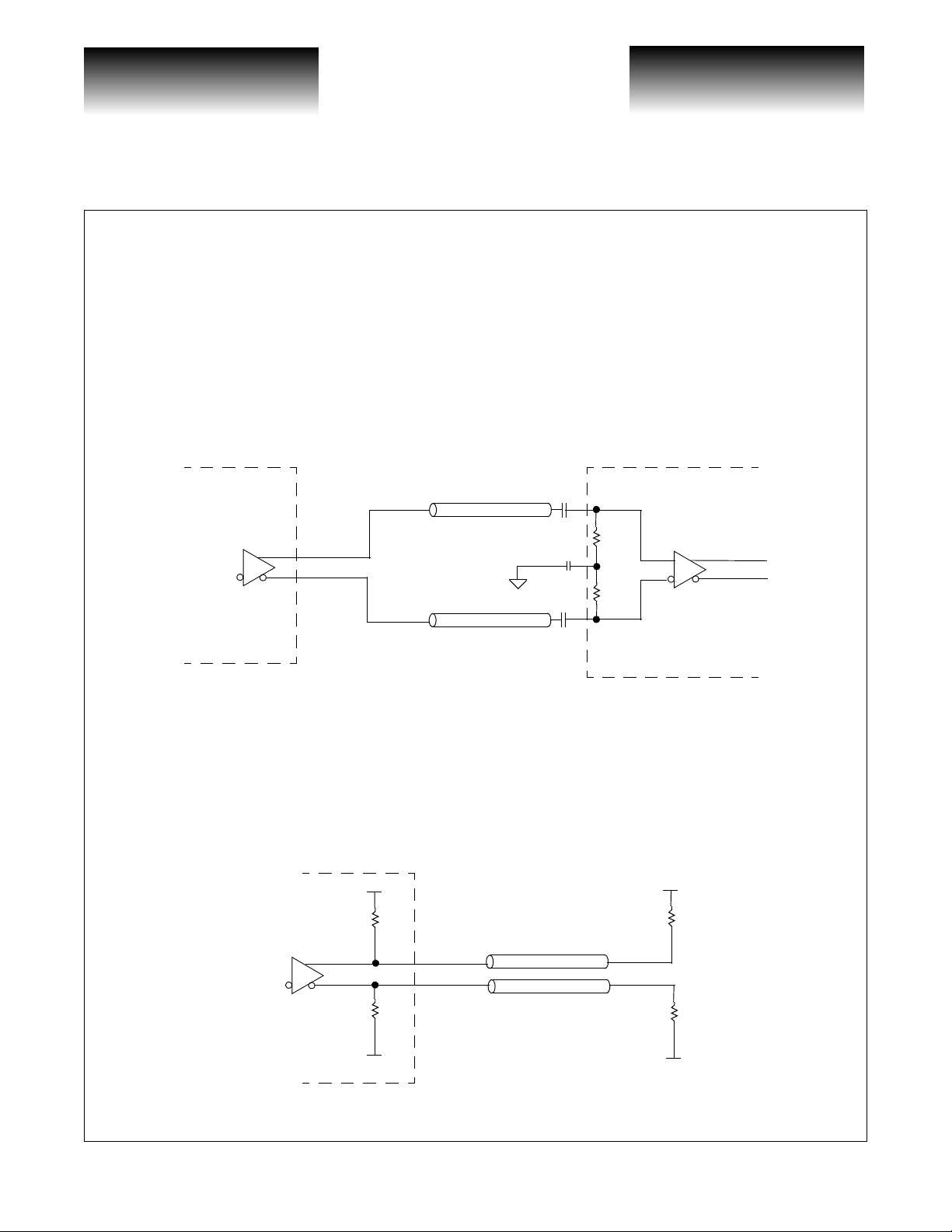
Two reference clock inputs are provided, REFCK1 and REFCK0, to allow “on-the-fly sw itchin g” between
SONET and Gigabit Ethernet applications if desired. Sin ce SONET and Gigabit Ethernet require d if ferent reference clock frequencies, the VSC8122 allows the user to toggle between the two reference clock frequencies
(REFCK1 and REFC K0 ) to su pply the ap pr opria t e in put c loc k. RE F_INP UTS E L is us ed to to ggl e be tw een th e
two reference clock input frequencies; REF_INPUTSEL= “0” selects REFCK0 and REF_INPUTSEL= “1”
selects REFCK1. Either reference cl ock i nput (R EFCK1, REF CK0) can be used for SONET o r Giga bit Et hernet
reference frequencies. LVPECL levels are recommended for REFCK inputs (see Figure 4). If a reference clock
is unused, it is recommended that one of its inputs be tied to V
GND through a 5.1k
Ω resistor.
Figure 4: REFCK Input Levels
through a 5.1kΩ resistor, the other one to
CC
LVPECL Level REFCK Inputs (recommended)
NON- LVPECL Level REFCK Inputs
0.1µf
REFCK0 /
REFCK1
50Ω
(1)
VCC-2
NOTES: (1) For differential REFC K input sig nals, 100 Ω termination between true and compleme nt REFCK signals c an be
substituted for the 50
(2) With the input ac-coupled, V
VSC8122
Ω to V
TERM
termination on each line.
can be to any power supply required for the upstream device.
TERM
REFCK0 /
REFCK1
V
TERM
VSC8122
50Ω
(1, 2)
Page 4 G52228-0, Rev 4.1
© VITESSE SEMICONDUCTOR CORPORATION • 741 Ca l le Pl an o • Camarillo, CA 93012
Tel: (800) VITESSE • FAX: (805) 987-5896 • Email: prodinfo@vitesse.com
Internet: www.vitesse.com
01/05/01
Page 5
VITESSE
SEMICONDUCTOR CORPORATION
Data Sheet
VSC8122
Table 2: Reference Frequency
Reference Frequency REF_SEL0 REF_SEL1
19.44MHz (19.53MHz) 0 0
38.88MHz (39.06MHz) 1 0
77.76MHz (78.13MHz) 0 1
155.52MHz (156.25MHz) 1 1
Loop Filter
Multi-Rate SONET/SDH
Clock and Data Recovery IC
The Phase-Lock Loop (PLL) on the VSC81 22 employs two external capacitors. The PLL de sign is fully
differential, therefore the loop filter must also be fully differential. One capacitor should be connected between
FILTAO and FILTAI, with the other connected between FILTAON and FILTAIN. Recommended capacitors are
low-inductance 1.0
µF (0603 or 0805) ceramic SMT X7R devices, 6.3 WVDC or greater, with tolerance of 10%
or better.
AC Characteristic s (Over recommended operating conditions)
Table 3: AC Characteristics
Parameters Description Min Typ Max Units Conditions
t
pd
t
r,tf
t
r,tf
Jitter
gen
Jitter
tol
LBW Loop Bandwidth ——2.0 MHz -3dB point of jitter transfer curve
Jitter
peak
Center of output da ta eye from
rising edge of CO+
DO± rise and fall times ——150 ps 20% to 80% into 50Ω load.
CO± rise and fall times ——135 ps 20% to 80% into 50Ω load.
Jitter Generation (12kHz20MHz)
Jitter Tolerance ————Exceeds SONET/SDH mask
Jitter Peaking ——0.1 dB
-75 — +75 ps
——3.6 ps - rms
Measured at the HS data output for
jitter in the 12kHz - 20MHz band.
Assume 1.2ps rms input data jitter.
G52228-0, Rev 4.1 Page 5
01/05/01
© VITESSE SEMICONDUCTOR CORPORATION • 741 Calle Plano • Camarillo, CA 93012
Tel: (800) VITESSE • FAX: (805) 987-5896 • Email: prodinfo@vitesse.com
Internet: www.vitesse.com
Page 6

VITESSE
SEMICONDUCTOR CORPORATION
Multi-Rate SONET/SDH
Clock and Data Recovery IC
Figure 5: High-Speed Clock and Data Outputs
80%
Data Output
20%
tR, t
F
t
PD
80%
Clock Output
t
t
R
F
Table 4: High-Speed Inputs and Outputs
Parameters Description Min Typ Max Units Conditions
∆V
∆V
V
V
R
OD
OC
CMO
DIFF
IN
Data output voltage swing 600 900 1000 mV
Clock output v oltage swing 500 700 1000 mV
Common-mode range (DO/CO) 2.6 — 3.2 V
Serial input absolute v oltage, single
250 — 1200 mV AC-coupled
ended peak-to-peak swing (V
) for DI +/-
V
IL
Input resistance between DI+ an d
or DI- and V
V
TERM
TERM
-
IH
43 — 58 Ω
20%
Data Sheet
VSC8122
Table 5: PLL Parameters
Parameters Description Min Typ Max Units Conditions
REF_CLK Duty Cycle 45 — 55 %
REF_CLK Frequency Range -100 — +100 ppm
-
-
— VCC-
0.7
— VCC-
1.475
V
V
01/05/01
V
V
IH
V
IL
Page 6 G52228-0, Rev 4.1
REF_CLK Input High Voltage
REF_CLK Input Low Voltage
© VITESSE SEMICONDUCTOR CORPORATION • 741 Ca l le Pl an o • Camarillo, CA 93012
Tel: (800) VITESSE • FAX: (805) 987-5896 • Email: prodinfo@vitesse.com
CC
1.165
V
CC
2.0
Internet: www.vitesse.com
Page 7

VITESSE
SEMICONDUCTOR CORPORATION
Data Sheet
VSC8122
Multi-Rate SONET/SDH
Clock and Data Recovery IC
DC Characteristics (Over recommended operating conditions)
Table 6: TTL Inputs and Outputs
Parameters Description Min Typ Max Units Conditions
V
OH
V
OL
V
IH
V
IL
I
IH
I
IL
Table 7: Power Supply
Parameters Description Min Typ Max Units Conditions
V
CC
P
D
I
CC
Output HIGH voltage 2.4 ——VI
Output LOW voltage ——0.5 V IOL= 1.0mA
Input HIGH voltage 2.0 — 3.47 V
Input LOW voltage 0 — 0.8 V
Input HIGH current — 50 500 µAVIN = 2.4V
Input LOW current ——500 µAVIN = 0.5V
Supply voltage 3.14 3.3 3.47 V 3.3V± 5%
Power dissipation — 1.0 1.2 W Outputs terminated
Supply current — 300 347 mA Outputs terminated
= -1.0mA
OH
Absolute Maximum Ratings
(1)
Power Supply Voltage (VCC) ..........................................................................................................-0.5V to +3.8V
DC Input Voltage (differential inputs) ....................................................................................-0.5V to V
CC
+0.5V
DC Input Voltage (TTL inputs).......................................................................................................-0.5V to +5.5V
DC Output Voltage (TTL outputs) .........................................................................................-0.5V to V
+ 0.5V
CC
Output Current (TTL outputs).................................................................................................................. +/-50mA
Output Current (differential outputs)........................................................................................................+/-50mA
Case Temperature Under Bias......................................................................................................-55
NOTE: (1) CAUTION: Stress es lis te d un de r “Abs o lute Maximum Ratings” may be applied to devices on e at a tim e without caus-
ing permanent damage. Functionality at or above the values listed is not implied. Exposure to these values for extended
periods may affect device reliability.
o
C to +125oC
Recommended Operating Conditions
Power Supply Voltage, (VCC) .............................................................................................................+3.3V+5%
Operating Temperature Range ........................................................0
o
C Ambient to +85oC Case Temperature
ESD Ratings
Proper ESD procedures shoul d be used when handl ing t his pr oduct. Th e VSC812 2 is r ated t o the fol lo wing E SD
voltages based on the human body model:
1. All pins are rated at or above 1500V.
G52228-0, Rev 4.1 Page 7
01/05/01
© VITESSE SEMICONDUCTOR CORPORATION • 741 Calle Plano • Camarillo, CA 93012
Tel: (800) VITESSE • FAX: (805) 987-5896 • Email: prodinfo@vitesse.com
Internet: www.vitesse.com
Page 8

VITESSE
SEMICONDUCTOR CORPORATION
Multi-Rate SONET/SDH
Clock and Data Recovery IC
Package Pin Descriptions
Top View
FSEL0
FSEL1
REF_INPUTSEL
N/C
VEE_ANA
VCC_ANA
N/C
N/C
LOL
NOREF
VCC
FILTAO
FILTAI
FILTAIN
FILTAON
VEE
1
3
5
7
9
11
13
15
Figure 6: Pin Diagram
N/C
VCC
N/C
VEE
VCC
63 61 59 57 55 53 51 49
DI+
VTERM
DI-
VCC
VCC
VCC
REFSEL1
VEE
VEE
VITESSE
VSC8122
17 19 21 23 25 27 29 31
Data Sheet
VSC8122
REFSEL0
VCC
VEE
47
45
43
41
39
37
35
33
REFCLK0+
REFCLK0REFCLK+
REFCLK1VEE
VCC
VEE
VCC
DO+
DOVCC
VEE
VCC
N/C
N/C
N/C
N/C
VCC
Page 8 G52228-0, Rev 4.1
© VITESSE SEMICONDUCTOR CORPORATION • 741 Ca l le Pl an o • Camarillo, CA 93012
Tel: (800) VITESSE • FAX: (805) 987-5896 • Email: prodinfo@vitesse.com
N/C
N/C
N/C
N/C
VCC
Internet: www.vitesse.com
CO-
VEE
CO+
VCC
VCC
N/C
VEE
VCC
01/05/01
Page 9

VITESSE
SEMICONDUCTOR CORPORATION
Data Sheet
VSC8122
Table 8: Pin Identifications
Pin # Name I/O Level Description
1 FSEL0 I TTL
2 FSEL1 I TTL
3 REF_INPUTSEL I TTL
4NC——
5 VEE_ANA I GND typ.
6 VCC_ANA I +3.3V typ.
7NC——
8NC——
9LOLOTTL
10 NOREF O TTL
11 VCC I +3.3V typ.
12 FILTAO I —
13 FILTAI I —
14 FILTAIN I —
15 FILTAON I —
16 VEE I GND typ.
17 VCC I +3.3V typ.
18 NC ——
19 NC ——
20 NC ——
21 NC ——
22 NC ——
23 NC ——
24 VCC I +3.3V typ.
25 VEE I GND typ.
26 VCC I +3.3V typ.
27 CO- O HS
28 CO+ O HS
29 VCC I +3.3V typ.
30 VEE I GND typ.
31 VCC I +3.3V typ.
32 NC ——
33 NC ——
34 NC ——
Selectable input rate pin 0
Selectable input rate pin 1
Toggle between REFCK1 and REFCK0
No connect, leave unconnected
Negative power supply pi ns for anal og parts of CM U
Positive power supply pins for analog parts of CMU
No connect, leave unconnected
No connect, leave unconnected
Loss of lock indication
No reference output. Active HIGH for REFCK far off the
expected frequency.
Positive power supply
Loop filter pin - connect via capacitor to FILTAI
Loop filter pin - connect via capacitor to FILTAO
Loop filter pin - connect via capacitor to FILTAON
Loop filter pin - connect via capacitor to FILTAIN
Negative power supply
Positive power supply
No connect, leave unconnected
No connect, leave unconnected
No connect, leave unconnected
No connect, leave unconnected
No connect, leave unconnected
No connect, leave unconnected
Positive power supply
Negative power supply
Positive power supply
High-speed clock output, complement
High-speed clock output, true
Positive power supply
Negative power supply
Positive power supply
No connect, leave unconnected
No connect, leave unconnected
No connect, leave unconnected
Multi-Rate SONET/SDH
Clock and Data Recovery IC
(1)
(1)
(1)
(1)
(1)
(1)
(1)
(1)
(1)
(1)
G52228-0, Rev 4.1 Page 9
01/05/01
© VITESSE SEMICONDUCTOR CORPORATION • 741 Calle Plano • Camarillo, CA 93012
Tel: (800) VITESSE • FAX: (805) 987-5896 • Email: prodinfo@vitesse.com
Internet: www.vitesse.com
Page 10

VITESSE
SEMICONDUCTOR CORPORATION
Multi-Rate SONET/SDH
Clock and Data Recovery IC
Pin # Name I/O Level Description
35 VCC I +3.3V typ.
36 VEE I GND typ.
37 VCC I +3.3V typ.
38 DO- O HS
39 DO+ O HS
40 VCC I +3.3V typ.
41 VEE I GND typ.
42 VCC I +3.3V typ.
43 VEE I GND typ.
44 REFCK1- I LVPECL
45 REFCK1+ I LVPECL
46 REFCK0- I LCPECL
47 REFCK0+ I LVPECL
48 VEE I GND typ.
49 VCC I +3.3V typ.
50 REF_SEL[0] I —
51 REF_SEL[1] I —
52 VCC I +3.3V typ.
53 VEE I GND typ.
54 VEE I GND typ.
55 VCC I +3.3V typ.
56 DI- I HS
57 DI+ I HS
58 VCC I +3.3V typ.
59 VTERM I 0V->3.3V
60 VEE I GND typ.
61 VCC I +3.3V typ.
62 NC ——
63 VCC I +3.3V typ.
64 NC ——
NOTE: (1) No connect (NC) pins must be left unconnected, or floating. Connecting any of these pins to either the positive or neg-
ative power supply rails may ca use improper operation or failure of the device, or in extreme cases, cause p ermanent
damage to the device.
Positive power supply
Negative power supply
Positive power supply
High-speed data output, complement.
High-speed data output, true
Positive power supply
Negative power supply
Positive power supply
Negative power supply
Reference clock 1 input, complement
Reference clock 1 input, true
Reference clock 0 input, complement
Reference clock 0 input, true
GND power supply
Positive power supply
Reference clock rate select pin 0
Reference clock rate select pin 1
Positive power supply
Negative power supply
Negative power supply
Positive power supply
High-speed data input, complement
High-speed data input, true
Positive power supply
High-speed data input termination voltage (may be connected
to ground through a series AC-coupling capacitor)
Negative power supply
Positive power supply
No connect, leave unconnected
Positive power supply
No connect, leave unconnected
(1)
Data Sheet
VSC8122
Page 10 G52228-0, Rev 4.1
© VITESSE SEMICONDUCTOR CORPORATION • 741 Ca l le Pl an o • Camarillo, CA 93012
Tel: (800) VITESSE • FAX: (805) 987-5896 • Email: prodinfo@vitesse.com
Internet: www.vitesse.com
01/05/01
Page 11

VITESSE
SEMICONDUCTOR CORPORATION
Data Sheet
VSC8122
Package Information
F
G
64 49
1
16
Multi-Rate SONET/SDH
Clock and Data Recovery IC
64-pin PQFP Package Drawing
Item
48
L
IH
33
A2.45MAX
D 2.00 +0.10
E0.22 ±.05
F 13.20 ±.25
G 10.00 ±.10
H 13.20 ±.25
I 10.00 ±.10
J0.88 ±.15
K0.50BASIC
10
mm
Tol.
A
0.30 RAD.TYP.
10oTYP
100TYP
0.20 RAD
3217
A
. TYP.
0.17 MAX.
0.25
D
K
STANDOFF
0.25 MAX.
o
0o- 8
J
E
NOTES:
Drawing not to scale.
Heat spreader up on 10mm package only.
All units in mm unless otherwise noted.
Heat spreader is not electrically connected.
Package #: 101-XXX-X
Issue #: 1
0.102 MAX. LEAD
COPLANARITY
Package #: 101-XXX-X
Issue #: 1
G52228-0, Rev 4.1 Page 11
01/05/01
© VITESSE SEMICONDUCTOR CORPORATION • 741 Calle Plano • Camarillo, CA 93012
Tel: (800) VITESSE • FAX: (805) 987-5896 • Email: prodinfo@vitesse.com
Internet: www.vitesse.com
Page 12

VITESSE
SEMICONDUCTOR CORPORATION
Multi-Rate SONET/SDH
Clock and Data Recovery IC
Data Sheet
VSC8122
Package Thermal Considerations
This package has been enhanced with a copper heat slug to provide a low thermal resistance path from the
die to the exposed surface of the heat spreader. The thermal resistance is shown in the following table:
Table 9: Thermal Resistance
Symbol Description
θ-jc Thermal resistance from junction to case. 1.5
θ-ca
Thermal Resistance With Airflow
Shown in the table below is the thermal resistance wi th airflo w. This thermal resistance value reflects all the
thermal paths including through the leads in an environment where the leads are exposed. The temperature difference between the amb ient airfl ow temperature and the ca se temperatur e should be the wors t case power of
the device multiplied by the thermal resistance.
Thermal resistance from case to ambient with no airflow,
including conduction through the leads.
o
C/W
31.5
Table 10: Thermal Resistance With Airflow
Airflow θ-ca (oC/W)
100 lfpm 25.8
200 lfpm 23.0
400 lfpm 19.3
600 lfpm 17.0
Maximum Ambient Temperature Without Heatsink
The worst case ambient temperature without use of a heatsink is given by the equation:
T
A(MAX)
where:
θ
= Theta case to ambient at appropriate airflow
CA
T
A(MAX)
T
C(MAX)
P
(MAX)
= Ambient Air temperature
= Case temperature (85oC for VSC8122)
= Power (1.2W for VSC8122)
= T
C(MAX)
- P
(MAX)θCA
Page 12 G52228-0, Rev 4.1
© VITESSE SEMICONDUCTOR CORPORATION • 741 Ca l le Pl an o • Camarillo, CA 93012
Tel: (800) VITESSE • FAX: (805) 987-5896 • Email: prodinfo@vitesse.com
Internet: www.vitesse.com
01/05/01
Page 13

VITESSE
SEMICONDUCTOR CORPORATION
Data Sheet
VSC8122
Table 11: Maximum Ambient Air Temperature Without Heatsink
Airflow T
Still air 47.2
100 lfpm 54.0
200 lfpm 57.4
400 lfpm 61.8
600 lfpm 64.6
Note that ambient air temperature varies throughout the system based on the positioning and magnitude of
heat sources and the direction of air flow.
Order ing Information
The order number for this product is formed by a combination of the device number, and package type.
Device Type
VSC8122: OC-3/12/48 (STM-1/4/16)
Clock and Data Recovery
A(MAX)
VSC8122
oC
QP
Package Style
QP: 64-pin, 10 x 10 mm PQFP
Multi-Rate SONET/SDH
Clock and Data Recovery IC
Notice
Vitesse Semiconductor Corporation (“Vitesse”) provides this document for informational purposes only. All information in this document, including descriptions of features, functions, performance, technical specifications and availability, is subject to change without notice at any time. Nothing contained in this docum ent shall be construed a s extending any warra nty or promis e, express or impl ied, that any Vitesse product wil l be
availab le as de scr i be d or will be suitable for or will accomplish an y par ti cu lar task.
Vitesse products are not intended for use in life support applianc es, devices or syste m s. Use of a Vitesse product in such applications without written consent is prohibited.
G52228-0, Rev 4.1 Page 13
01/05/01
© VITESSE SEMICONDUCTOR CORPORATION • 741 Calle Plano • Camarillo, CA 93012
Tel: (800) VITESSE • FAX: (805) 987-5896 • Email: prodinfo@vitesse.com
Internet: www.vitesse.com
Page 14

VITESSE
SEMICONDUCTOR CORPORATION
Multi-Rate SONET/SDH
Clock and Data Recovery IC
Data Sheet
VSC8122
Page 14 G52228-0, Rev 4.1
© VITESSE SEMICONDUCTOR CORPORATION • 741 Ca l le Pl an o • Camarillo, CA 93012
Tel: (800) VITESSE • FAX: (805) 987-5896 • Email: prodinfo@vitesse.com
Internet: www.vitesse.com
01/05/01
 Loading...