

Page 1
VITESSE
SEMICONDUCTOR CORPORATION
Data Sheet
VSC8121
2.488GHz SONET/SDH
Clock Generator
Features
• Monolithic Phase Locked Loop
• On-Chip LC Oscillator
• On-Chip Loop Filter
• TTL/CMOS Reference Clock
• Selectable Reference
• Jitter Meets SONET OC-48 and
SDH STM-16 Requirements
• High-Speed CML Clock Output
• Single 3.3V Supply
• Compact 10mm x 10mm 44 Pin PQFP Package
General Description
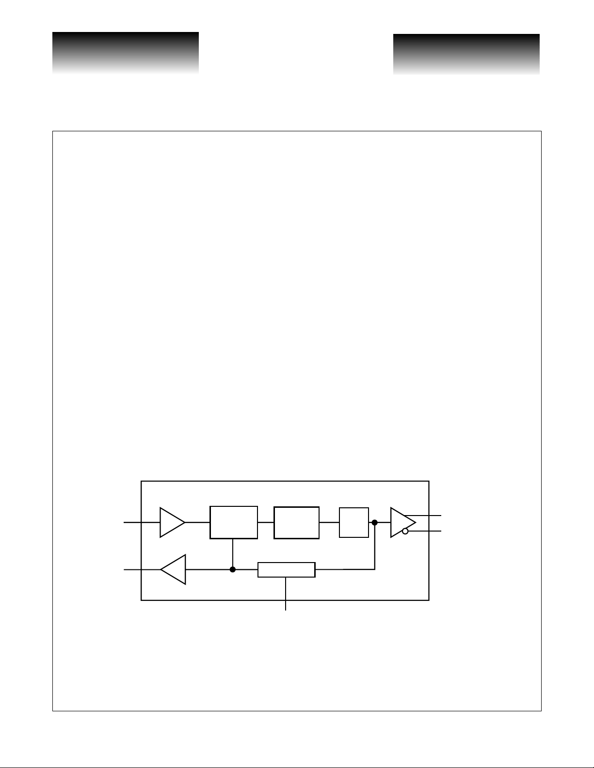
The VSC8121 is a monolithic Phase Locked Loop (PLL) based clock generator designed for telecommunications systems operating at 2.5Gb /s. The VSC 8121 inco rporates a reactanc e-based (LC) Voltage Contr olled
Oscillator (VCO) with low phase noise. The PLL’s loop filter is on-chip.
The device has a differential 2.488GHz CML clock output (CO/CON) signal, a single-ended TTL lowspeed clock (LSCLK) output equivalent in frequency to that of the reference clock, and a TTL reference clock
input selectable for 51.84MHz, 77.76MHz or 155.52MHz. TTL inputs REFSEL[0:1] are used to make this
selection.
A clean REFCLK signal is required since jitter below the PLL loop bandwidth, which is present on the
REFCLK input, will appear on the output. Jitter on REFCLK at frequencies above the loop bandwidth will be
attenuated by the PLL. The state of REFSEL[0:1] will select which frequency is expected on the REFCLK
input.
VSC8121 Functional Block Diagram
REFCLK
LSCLK
G52163-0, Rev 4.2 Page 1
04/16/01
© VITESSE SEMICONDUCTOR CORPORATION • 741 Calle Plano • Camarillo, CA 93012
Tel: (800) VITESSE • FAX: (805) 987-5896 • Email: prodinfo@vitesse.com
Ph.Freq.
Detector
Loop
Filter
Divider
REFSEL[0:1]
Internet: www.vitesse.com
VCO
CO
CON
CLOCK
OUT
Page 2

VITESSE
SEMICONDUCTOR CORPORATION
2.488GHz SONET/SD H
Clock Generator
Data Sheet
VSC8121
Applications Information
High-Speed Clock Output
The differentia l cloc k outp ut waveforms p roduce d by t he VSC8121 ar e sin usoidal i n natu re, by design. This
typically results in less n oise gener ation t han square pu lses in most cu stomer applicat ions. Fi gure 1 shows a t ypical, single-ended clock output waveform produced by the device.
Figure 1: Typical Clock Output (CO) Waveform
75mV/div
100ps/div
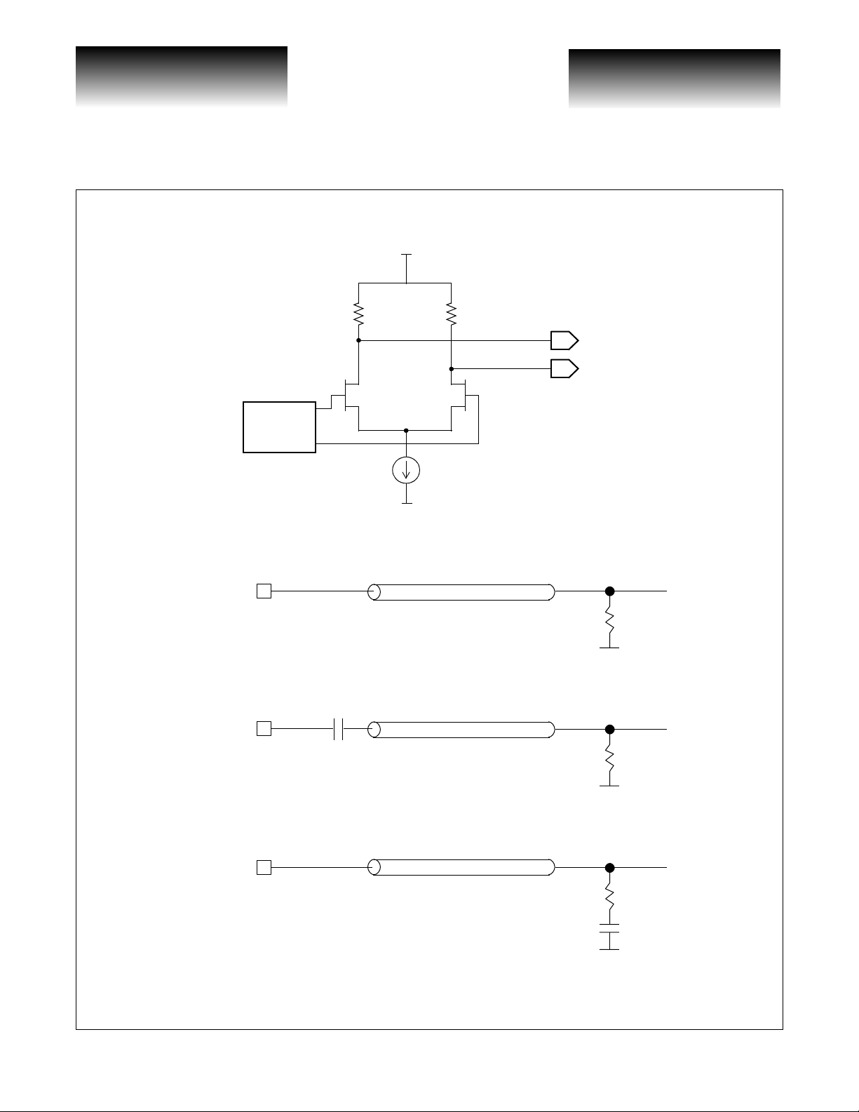
CO and CON are high-speed CML outp uts. As sho wn in Figu re 2, the ou tput dri ver consist s of a dif fe rential
pair designed to drive a 50
50
Ω on-chip to prevent reflections.
Careful layout of these signals is required for optimal performance. Figure 3 demonstrates various termination methods that may be employed, depending on the particular application. Either DC-coupling (termination
#1 in Figure 3) or one of two AC coupling methods (terminati ons #2 and #3) may be used. As indicate d, Vitesse
recommends termination #2 for AC-coupling.
Ω transmission line environment. Note that the output driver is back terminated to
Page 2 G52163-0, Rev 4.2
© VITESSE SEMICONDUCTOR CORPORATION • 741 Ca l le Pl an o • Camarillo, CA 93012
Tel: (800) VITESSE • FAX: (805) 987-5896 • Email: prodinfo@vitesse.com
Internet: www.vitesse.com
04/16/01
Page 3
VITESSE
SEMICONDUCTOR CORPORATION
Data Sheet
VSC8121
Figure 2: High-Speed Clock Output Diagram
V
CC
50Ω
Pre-Driver
50Ω
V
EE
2.488GHz SONET/SDH
Clock Generator
CO
CON
1)
CO/CON
2)
CO/CON
3)
CO/CON
Figure 3: Example High-Speed CML Clock Output Terminations
(Recommended for DC-Coupling)
VCC
0.01 µf
V
TERM
V
50 Ω
50 Ω
TERM
(Recommended for AC-Coupling)
(Alternative for AC-Coupling)
50 Ω
0.01 µf
G52163-0, Rev 4.2 Page 3
04/16/01
© VITESSE SEMICONDUCTOR CORPORATION • 741 Calle Plano • Camarillo, CA 93012
Tel: (800) VITESSE • FAX: (805) 987-5896 • Email: prodinfo@vitesse.com
Internet: www.vitesse.com
Page 4

VITESSE
SEMICONDUCTOR CORPORATION
2.488GHz SONET/SD H
Clock Generator
Reference Clock Input
The input stage at the REFCLK input pin consists of ESD protection, followed by a current limiting circuit
which precedes a driver responsible for providing the signal to the phase frequency detector. As pictured below
in Figure 4, the driver has a high impedance, FET gate input. The additional resistance contributed by the current limiting circuit is relatively negligi ble.
Figure 4: Reference Clock Input Diagram
VCC
REFCLK
VEE
Current
Limiting
VTT
Data Sheet
VSC8121
Care should be taken in selection of the reference clock. Time jitter on the reference clock which is within
the PLL’s loop bandwidth will appear on the 2.5G Hz output. Telecom quality crystal oscillators from vendors
such as Connor-Winfield or Vectron are suitable.
Table 1: Reference Clock Selection
REFSEL[1] REFSEL[0]
0 0 51.84MHz 2500KHz
1 0 77.76MHz 3000KHz
Don’t Care 1 155.52MHz 5500KHz
Die Usage
Vitesse optionally provides this device in unpackaged, die-only format for multi-chip module and related
applications. For further informtion, please contact Vitesse.
Selected Reference
Frequency
Typical
Loop Bandwidth
Page 4 G52163-0, Rev 4.2
© VITESSE SEMICONDUCTOR CORPORATION • 741 Ca l le Pl an o • Camarillo, CA 93012
Tel: (800) VITESSE • FAX: (805) 987-5896 • Email: prodinfo@vitesse.com
Internet: www.vitesse.com
04/16/01
Page 5

VITESSE
SEMICONDUCTOR CORPORATION
Data Sheet
VSC8121
2.488GHz SONET/SDH
Clock Generator
AC Characteristics
T a ble 2: AC Characteristics
Parameter Description Min Typ Max Units Conditions
T
CLK
RC
d
RC
f
∆f
RC
t
jitter
NOTE: (1) ppm refers to “p arts per mi llion. ” 100 ppm (1 00/100 0000) is equ ivalen t to 0 .01%. Therefore, the equiv alen t reference
clock frequency range in MHz for +/-100ppm tolerance is as follows:
High-speed output clock period — 401.9 — ps
Reference clock duty cycle 45 — 55 %
51.84,
Reference clock frequency (selectable) —
77.76,
or
— MHz
155.52
Reference clock frequency tolerance -100 — +100 ppm
Jitter generation — 1.75 3.6 ps RMS
RC
f
X 100ppm = Acceptable Range
(1)
12kHz to 20MHz.
See Figure 5.
51.84MHz 5.184KHz 51.83MHz to 51.85MHz
77.76MHz 7.776KHz 77.75MHz to 77.78MHz
155.52MHz 15.552KHz 155.51MHz to 155.54MHz
Note that +/-100ppm tolerance for reference clock frequency more than accommodates the SONET/SDH requirement that refer-
ence clock-supplying crystals function at +/-20ppm.)
Figure 5: RMS/Peak-to-Peak Jitter (12kHz - 20MHz), REF_CLK freq = 77.76MHz
3.0
2.5
2.0
1.5
ps
1.0
0.5
0.0
0
RMS Jitter Pk-Pk Jitter
25
20
15
ps
10
5
20 40
Case Temperature (deg C)
100
80
60
0
0
20 40
Case Temperature (deg C)
60
100
80
G52163-0, Rev 4.2 Page 5
04/16/01
© VITESSE SEMICONDUCTOR CORPORATION • 741 Calle Plano • Camarillo, CA 93012
Tel: (800) VITESSE • FAX: (805) 987-5896 • Email: prodinfo@vitesse.com
Internet: www.vitesse.com
Page 6

VITESSE
SEMICONDUCTOR CORPORATION
2.488GHz SONET/SD H
Clock Generator
DC Characteristics
T able 3: Low Speed I/O
Parameter Description Min Typ Max Units Conditions
V
OH
V
OL
V
IH
V
IL
I
IH
I
IL
T able 4: High-Speed Differential Outputs
Parameter Description Min Typ Max Units Conditions
V
OD
V
OCM
Note: Output jitter characteristics apply for differential outputs.
Output HIGH voltage (TTL) 2.4 ——VIOH = -1.0 mA
Output LOW voltage (TTL) ——0.5 V IOL = +1.0 mA
Input HIGH voltage (TTL) 2.0 — 3.47 V —
Input LOW voltage (TTL) 0 — 0.8 V —
Input HIGH current (TTL) — 50 500 µAVIN = 2.4V
Input LOW current (TTL) ——-500 µAVIN = 0.5V
Output differential voltage 450 — 800 mV
Output common-mod e voltage
V
0.40
V
0.80
V
0.80
CC
CC
CC
-
—
-
—
-
—
V
0.25
V
0.50
V
0.50
CC
CC
CC
mV
mV
mV
T e r mi na tio n #1
(See Figure 3)
T e r mi na tio n #2
(See Figure 3)
T e r mi na tio n #3
(See Figure 3)
Data Sheet
VSC8121
Table 5: Power Supply Currents
Parameter Description Min Typ Max Units Conditions
I
CC
P
D
Power supply current from V
Power dissipation 0.7 W Outputs Open
CC
200 mA Outputs Open
Page 6 G52163-0, Rev 4.2
© VITESSE SEMICONDUCTOR CORPORATION • 741 Ca l le Pl an o • Camarillo, CA 93012
Tel: (800) VITESSE • FAX: (805) 987-5896 • Email: prodinfo@vitesse.com
Internet: www.vitesse.com
04/16/01
Page 7

VITESSE
SEMICONDUCTOR CORPORATION
Data Sheet
VSC8121
Absolute Maximum Ratings
Power Supply Voltage (VCC) Potential to GND............................................................................-0.5 V to +4.0 V
TTL Input Vo ltage Applied ..........................................................................................................-0.5 V to + 5.5V
Output Current (I
Case Temperature Under Bias (T
Storage Temperature (T
NOTE: (1) Caution: Stresses listed under “Absolute Ma x imu m Ra ti ng s” may be applied to de vice s one a t a time without caus ing p erm a-
nent damage. Functionality at or exceeding the values listed is not implied. Exposure to these values for extended periods may
affect device reliability.
)...................................................................................................................................50 mA
OUT
)................................................................................................-55o to + 125oC
C
) ........................................................................................................... -65o to + 150oC
STG
(1)
2.488GHz SONET/SDH
Clock Generator
Recommended Operating Conditions
Power Supply Voltage (VCC).................................................................................................................+3.3V ±5%
Commercial Operating Temperature Range
NOTE: (1) Lower limit of specification is ambient temperature and upper limit is case temperature.
(1)
(T)............................................................................... 0oC to 85oC
ESD Ratings
Proper ESD procedures should be used when handling this product. The VSC8121 is rated to the following
ESD voltages based on the human body model:
1. All pins are rated at or above 1500V.
Note: If used singl e -ended, the unused output should be terminated.
G52163-0, Rev 4.2 Page 7
04/16/01
© VITESSE SEMICONDUCTOR CORPORATION • 741 Calle Plano • Camarillo, CA 93012
Tel: (800) VITESSE • FAX: (805) 987-5896 • Email: prodinfo@vitesse.com
Internet: www.vitesse.com
Page 8

VITESSE
SEMICONDUCTOR CORPORATION
2.488GHz SONET/SD H
Clock Generator
Package Pin Descriptions
NC
NC
NC
NC
1
2
3
4
Figure 6: Pin Diagram
VCCANA
NC
NCNCNC
44 43 42 41 40 39 37
NC
NC
VEEANA
NC
3638
NC
NC
35 34
33
32
31
30
Data Sheet
VSC8121
NC
NC
NC
VCCP
NC
NC
NC
VCCT
NC
NC
NC
5
6
7
8
9
10
11
12 13 14 15 16 17 18 19 20
NC
NC
NC
VEET
REFCLK
REFSEL0
REFSEL1
29
28
27
26
25
24
23
21 22
NC
LSCLK
VEE
NC
CON
CO
VCC
NC
NC
NC
NC
Page 8 G52163-0, Rev 4.2
© VITESSE SEMICONDUCTOR CORPORATION • 741 Ca l le Pl an o • Camarillo, CA 93012
Tel: (800) VITESSE • FAX: (805) 987-5896 • Email: prodinfo@vitesse.com
Internet: www.vitesse.com
04/16/01
Page 9

VITESSE
SEMICONDUCTOR CORPORATION
Data Sheet
VSC8121
Table 6: Package Pin Identification
Signal Name Pin # I/O Level Description
NC 1 - - Do not connect, leave open
NC 2 - - Do not connect, leave open
NC 3 - - Do not connect, leave open
NC 4 - - Do not connect, leave open
NC 5 - - Do not connect, leave open
NC 6 - - Do not connect, leave open
NC 7 - - Do not connect, leave open
V
CCT
NC 9 - - Do not connect, leave open
NC 10 - - Do not connect, leave open
NC 11 - - Do not connec t, leave open
NC 12 - - Do not connect, leave open
NC 13 - - Do not connect, leave open
V
EET
REFCLK 16 TTL Input TTL Reference Clock
REFSEL[0] 17 TTL Input TTL Selects Reference Frequency
REFSEL[1] 18 TTL Input TTL Selects Reference Frequency
LSCLK 19 TTL Output TTL Low Speed PLL Output
V
EE
NC 21 - - Do not connect, leave open
NC 22 - - Do not connect, leave open
NC 23 - - Do not connect, leave open
NC 24 - - Do not connect, leave open
NC 25 - - Do not connect, leave open
NC 26 - - Do not connect, leave open
V
CC
CO 28 Output 2.7 - 3.3V High-Speed Clock Out
CON 29 Output 2.7 - 3.3V High-Speed Clock Out Complement
V
CCP
NC 31 - - Do not connect, leave open
NC 32 - - Do not connect, leave open
NC 33 - - Do not connect, leave open
NC 34 - - Do not connect, leave open
NC 35 - - Do not connect, leave open
NC 36 - - Do not connect, leave open
V
EEANA
V
CCANA
NC 39 - - Do not connect, leave open
2.488GHz SONET/SDH
Clock Generator
(1)
(1)
(1)
(1)
(1)
(1)
(1)
8 Positive Supply 3.3V Fo r TTL I/O
(1)
(1)
(1)
(1)
(1)
14 Negative Supply GND For TTL I/O
20 Negative Supply GND
(1)
(1)
(1)
(1)
(1)
(1)
27 Po sitive Supply 3.3V
30 Po sitive Supply 3.3V Supply for High-Speed Outputs
(1)
(1)
(1)
(1)
(1)
(1)
37 Negative Supply GND For Analog Section
38 Po sitive Supply 3.3V For Analog Section
(2)
(1)
(2)
G52163-0, Rev 4.2 Page 9
04/16/01
© VITESSE SEMICONDUCTOR CORPORATION • 741 Calle Plano • Camarillo, CA 93012
Tel: (800) VITESSE • FAX: (805) 987-5896 • Email: prodinfo@vitesse.com
Internet: www.vitesse.com
Page 10

VITESSE
SEMICONDUCTOR CORPORATION
2.488GHz SONET/SD H
Clock Generator
Signal Name Pin # I/O Level Description
NC 40 - - Do not connect, leave open
NC 41 - - Do not connect, leave open
NC 42 - - Do not connect, leave open
NC 43 - - Do not connect, leave open
NC 44 - - Do not connect, leave open
NOTE: (1) Leave unconnected. Terminating these pins to GND, VEE or otherwise may have an adverse effect on the performance
of the device. (2) VCC pins 30 and 38 a re internally connected to each other.
Data Sheet
VSC8121
(1)
(1)
(1)
(1)
(1)
Page 10 G52163-0, Rev 4.2
© VITESSE SEMICONDUCTOR CORPORATION • 741 Ca l le Pl an o • Camarillo, CA 93012
Tel: (800) VITESSE • FAX: (805) 987-5896 • Email: prodinfo@vitesse.com
Internet: www.vitesse.com
04/16/01
Page 11

VITESSE
SEMICONDUCTOR CORPORATION
Data Sheet
VSC8121
Package Information
44 34
1
11
10oTYP
G
2.488GHz SONET/SDH
Clock Generator
44-Pin PQFP Packa ge Drawing
F
Item mm Tol.
A2.45 MAX
33
L
IH
23
2212
D 2.00 +.10 / -.05
E0.35 ±.05
F 13.20 ±.25
G 10.00 ±.10
H 13.20 ±.25
I 10.00 ±.10
J 0.88 +.15 / -.10
J1 0.80 +.15 / -.10
K0.80BASIC
L3.56±.50 DIA.
10oTYP
D
K
0.30 RAD.TYP.
NOTES:
Drawing not to scale.
Heat spreader up.
All units in mm unless otherwise noted.
Package #: 101-299-1
Issue #: 1
A
0.20 RAD.TYP.
0o- 8
0.17 MAX.
0.25
J
1
J
G52163-0, Rev 4.2 Page 11
04/16/01
© VITESSE SEMICONDUCTOR CORPORATION • 741 Calle Plano • Camarillo, CA 93012
Tel: (800) VITESSE • FAX: (805) 987-5896 • Email: prodinfo@vitesse.com
Internet: www.vitesse.com
o
E
0.25 MAX.
0.102 MAX. LEAD
COPLANARITY
Page 12

VITESSE
SEMICONDUCTOR CORPORATION
2.488GHz SONET/SD H
Clock Generator
Data Sheet
VSC8121
Thermal Considerations
This package has been enhanced with a copper heat slug to provide a low thermal resistance path from the
die to the exposed surface of the heat spreader. The thermal resistance is shown in the Table 7.
T a ble 7: Thermal Resistance
Symbol Description
θ
JC
θ
CA
Thermal Resistance With Airflow
Thermal resistance from junction-to-case. 2.0
Thermal resista nce from c ase-to- ambient w ith no airf low , inc luding co nduction t hrough
the leads.
Shown in T able 8 i s the thermal resistance with airflow. This thermal resistance value reflects al l the thermal
paths including through the leads in an environment where the leads are exposed. The temperature difference
between the ambient airflow temperature and the case temperature should be t he worst-case power of the devi ce
multiplied by the thermal resistance.
T able 8: Thermal Resistance With Airflow
Airflow θCA (oC/W)
100 lfpm 28
200 lfpm 25
400 lfpm 21
600 lfpm 18
o
C/W
35.0
Maximum Ambient Temperature Without Heatsink
The worst case ambient temperature without use of a heatsink is given by the equation:
T
A(MAX)
= T
C(MAX)
- P
(MAX)θCA
where:
θ
CA
T
A(MAX)
T
C(MAX)
P
(MAX)
Table 9: Maximum Ambient Air Temperature Without Heatsink
Airflow T
100 lfpm 65
200 lfpm 68
400 lfpm 70
600 lfpm 72
= Theta case to ambient at appropriate airflow
= Ambient Air temperature
= Case temperature (85oC for VSC8121)
= Power (0.7W for VSC8121)
oC
A(MAX)
None 60
Note that ambient air temperature varies throughout the system based on the positioning and magnitude of
heat sources and the direction of air flow.
Page 12 G52163-0, Rev 4.2
© VITESSE SEMICONDUCTOR CORPORATION • 741 Ca l le Pl an o • Camarillo, CA 93012
Tel: (800) VITESSE • FAX: (805) 987-5896 • Email: prodinfo@vitesse.com
Internet: www.vitesse.com
04/16/01
Page 13

VITESSE
SEMICONDUCTOR CORPORATION
Data Sheet
VSC8121
2.488GHz SONET/SDH
Clock Generator
VSC8121 Evaluation Board
An evaluation board is available from Vitesse which can be used to characterize the performance of the
VSC8121 2.488GHz SONET/SDH Clock Generator. The following sections provide a layout for the board,
general notes regardin g usag e and descriptions of input/output port s , as well a s an ex ampl e equ ipme nt setu p. To
learn more about how to order this board for your evaluation needs, please contact your local Vitesse Sales
Office.
Figure 7: Top-view Layout of the VSC8121 Evaluation Board
J1
VITESSE
U2
J5
R1
R2
S1
S2
R3
J3
C2
11
22 12
23
1
44
34
33
J4
J6
L1
C8
Board dimensions:
3” x 2.75” x 0.06”
Component Values:
R1 = 10kΩ
R2 = 10kΩ
R3 = 11Ω
R4 = 0Ω
R5 = 0Ω
R6 = leave open
R7 = leave open
J7
JP1
C1
C4
J9
U1
R5
R7
C10
R4
R6
C9
VS8121EVA
REV. A
J8
C1 = 10µF
C2 = 10µF
C4 = 0.1µF
C8 = 0.1µF
C9 = 0.01µF
C10 = 0.01µF
L1 = TDK-CB50-1206 ferrite
G52163-0, Rev 4.2 Page 13
04/16/01
© VITESSE SEMICONDUCTOR CORPORATION • 741 Calle Plano • Camarillo, CA 93012
Tel: (800) VITESSE • FAX: (805) 987-5896 • Email: prodinfo@vitesse.com
Internet: www.vitesse.com
Page 14

VITESSE
SEMICONDUCTOR CORPORATION
2.488GHz SONET/SD H
Clock Generator
Figure 8: Location of Additional Components on Back Side of the VSC8121 Evaluation Board
Data Sheet
VSC8121
C5
C7
Component Values:
C3 = 0.1µF
C5 = 0.1µF
C3C6
C6 = 0.1µF
C7 = 0.1µF
Equipment for Typical Set-up
VSC8121 Evaluation Board
Signal Generator or 155.52MHz Crystal Oscillator
Digital Oscilloscope
DC Power Supply
Power Supply Settings
VCC Set to 3.3V (Current draw will be approximately 180mA)
Reference Clock
To provide a reference clock to the VSC8121, either a Signal Generator or telecom-quality Crystal Oscillator can be used. The REFCLK level should be near 900mV(RMS) and, as listed in Table 1 of this specification,
operate at either 51 .84MHz , 77.76MH z, or 15 5.52MH z. The eva luation boa rd is preco nfigure d to run with a
155.52MHz reference clock, but can be easily modified to accept one of the other two frequency choices.
Page 14 G52163-0, Rev 4.2
© VITESSE SEMICONDUCTOR CORPORATION • 741 Ca l le Pl an o • Camarillo, CA 93012
Tel: (800) VITESSE • FAX: (805) 987-5896 • Email: prodinfo@vitesse.com
Internet: www.vitesse.com
04/16/01
Page 15

VITESSE
SEMICONDUCTOR CORPORATION
Data Sheet
VSC8121
Table 10: REFSEL [0,1] Switch Settings (S1, S2) For Selected Reference Frequency
REFSEL[0]
(S1)
0 0 51.84MHz
0 1 77.76MHz
1Don’t Care 155.52MHz
As reiterated above, the selected reference frequency is determined by the TTL inputs REFSEL[0] and
REFSEL[1]. The board can be made to operate wit h a REFCLK of eit her 51.84MHz or 77.7 6MHz by closi ng or
opening the appropriate connections at locations S1 and S2. As indicated in Table 10, S1 controls REFSEL[0],
and S2 controls REFSEL[1]. Closing one of these connections shorts the corresponding REFSEL pin to VEE.
You may either place a permanent short across the desired pin, or place a switch in both locations to leave the
option of toggling to different reference clock settings. (As an example, to configure the device to expect a
77.76MHz frequency, you would place a short or close the switch across S1 and leave S2 open.)
Recommended Evaluation Board Connections
Chabin to Banana Jack Connections
• JP1 (2nd position) to positive terminal of VS1
REFSEL[1]
(S2)
Selected Reference Frequency
2.488GHz SONET/SDH
Clock Generator
• JP1 (4th position) to negative term inal of VS1
(Optionally, microcli p or othe r connectors can be used to rout e po w er as de eme d pra c tic al by the custo m e r)
SMA Cable Connections
• J5 (REFCLK) to the RF Out port of the Signal Generator, -or- you may leave J5 unconnected and place a
crystal oscillator in location U2 (see the Using A Crystal Oscillator section below)
• J7 (LSCLK) to the external TRIGGER input of the Digital O sci lloscope
• J8 (CON) to Ch 1 of the Digital Oscilloscope
• J9 (CO) to Ch 2 of the Digital Oscillosco pe
NOTE: Ports not listed are not required for normal operation of the device , and should be left unconnected.
Using a Crystal Oscillator
The board provid es an option for a crysta l oscillator if it is n ot desired to drive the reference clo ck signal
with a signal generator or other device. A telecom-quality 155.52MHz crystal is recommended, since the goal
should be to introduce the least amount of jitter into the input as possible. Certain frequencies of jitter (those
below the loop bandwidth of the PLL) introduced at the REFCLK input will appear directly at the output of the
device.
G52163-0, Rev 4.2 Page 15
04/16/01
© VITESSE SEMICONDUCTOR CORPORATION • 741 Calle Plano • Camarillo, CA 93012
Tel: (800) VITESSE • FAX: (805) 987-5896 • Email: prodinfo@vitesse.com
Internet: www.vitesse.com
Page 16

VITESSE
SEMICONDUCTOR CORPORATION
2.488GHz SONET/SD H
Clock Generator
Example Set-Up
Data Sheet
VSC8121
The figure below shows one possible set-up using the VSC8121 Evaluation Board and recommended connections listed above. In this configuration, the device receives its reference clock input from an external signal
generator supplying a 900mV(RMS) signal. As an alternative, a crystal oscillator may be used instead to provide this reference. The C O and CON (High-Speed Clock True and C ompl emen t) an d L SCLK si gnal s may th en
be viewed with the scope, as shown on channels 1 through 3. Alternatively, if only one output is being viewed
by the scope, a 50ohm termination should be used on the remaining output to achieve more accurate measurements.
Figure 9: Example Equipment Set-up Using the VSC8121 Evaluation Board
CLOCKOUT
(51.84, 77.76 or 155.52MHz)
CLOCKOUTN
TRIGGER
Pattern
Generator
Digital Sampling
Scope
900mV(RMS)
CH1 CH2
TRIGGER
Low Speed Clock (LSCLK)
High-Speed Clock (CO)
J9
VEE
(0V)
VCC
(3.3V)
J7
Reference Clock (REFCLK)
J5
Optional
Crystal
VITESSE
VSC8121
High-Speed Clock Complement (CON)
The intent of this section is to answer the most common questions surrounding the use of the VSC8121
Evaluation Board. Please contact your local sales office if there are any additional details that Vitesse Semiconductor can provide to help you make more efficient use of your evaluation board.
J8
Eval Board
Page 16 G52163-0, Rev 4.2
© VITESSE SEMICONDUCTOR CORPORATION • 741 Ca l le Pl an o • Camarillo, CA 93012
Tel: (800) VITESSE • FAX: (805) 987-5896 • Email: prodinfo@vitesse.com
Internet: www.vitesse.com
04/16/01
Page 17

VITESSE
SEMICONDUCTOR CORPORATION
Data Sheet
VSC8121
Ordering Informatio n
The order number for this product is formed by a combination of the device number, and package type.
Device Type
2.488GHz SONET/SDH Clock Generator
VSC8121
2.488GHz SONET/SDH
Clock Generator
xx
Package Style
QI: 44-pin, 10mm x 10 mm PQFP
Notice
Vitesse Semiconductor Corporation (“Vitesse”) provides this docume nt for informational purpo s es only. All information in this docume nt, including descriptions of features, functions, performance, technical specifications and availability, is subject to change without notice at any time. Nothing contained in this document shall be co nstrued as extend ing any warra nty or promise, express or implie d, that any Vitesse product will be
available as described or will be suitable for or will accomplish any partic ul ar task.
Vitesse products are not intended for use in life support applia nc es, devices or systems. Use of a Vitesse product in such applications without written consent is prohibited.
G52163-0, Rev 4.2 Page 17
04/16/01
© VITESSE SEMICONDUCTOR CORPORATION • 741 Calle Plano • Camarillo, CA 93012
Tel: (800) VITESSE • FAX: (805) 987-5896 • Email: prodinfo@vitesse.com
Internet: www.vitesse.com
Page 18

VITESSE
SEMICONDUCTOR CORPORATION
2.488GHz SONET/SD H
Clock Generator
Item
1 4.1 2/4/00 General Description 1 Add CML text to the clock output, Deleted PECL output
2 4.1 2/4/00 Features 1 Changed to High-Speed clock output
3 4.1 2/4/00 Application Info 2
4 4.1 2/4/00 Figure 3 3 Changed to High-Speed CML Clock output terminations
5 4.1 2/4/00 Table 4 6
6 4.1 2/4/00 Table 6 9,10 Added Level Column to I/O’s
7 4.1 2/4/00 Table 7 12 Changed Theta Juntion to Case to 2.0
8 4.1 2/4/00 Figure 16 Changed CH3 to Trigger
Rev
No.
Date
Revision History
Section/Figure/
Table
Data Sheet
VSC8121
Page Description
Add High-Speed CML outputs, Deleted PECL/ECL
clock outputs
Changed to High-Speed Differential outputs, deleted the
PECL/ECL outputs
Page 18 G52163-0, Rev 4.2
© VITESSE SEMICONDUCTOR CORPORATION • 741 Ca l le Pl an o • Camarillo, CA 93012
Tel: (800) VITESSE • FAX: (805) 987-5896 • Email: prodinfo@vitesse.com
Internet: www.vitesse.com
04/16/01
 Loading...