

Page 1

VITESSE
SEMICONDUCTOR CORPORATION
Data Sheet
SC8113
ATM/SONET/SDH 622 Mb/s Transceiver Mux/Demux
with Integrated Clock Generation and Clock Recovery
Features
• Operates at Either STS-3/STM-1 (155.52Mb/s)
or STS-12/STM-4 (622.08Mb/s) Data Rates
• Compatible with Industry ATM UNI Devices
• On Chip Clock Generation of the
622.08MHz High Speed Clock (Mux)
or
• On Chip Clock Recovery of the
622.08MHz High Speed Clock (Demux)
• 8 Bit Parallel TTL Interface
• SONET/SDH Frame Recovery
• Lock Detect for both CRU and CMU
155.52MHz
155.52MHz or
• Loss of Signal (LOS) Input & LOS Detection
• +3.3V/5V programmable PECL Serial Interface
• Provides Equipment, Facilities and Split Loopback Modes as well as Loop Timing Mode
• Provide TTL & PECL reference clock inputs
• Meets Bellcore, ITU and ANSI Specifications for
Jitter Performance
• Low Power - 1.0 Watts Typical
• 100 PQFP Package
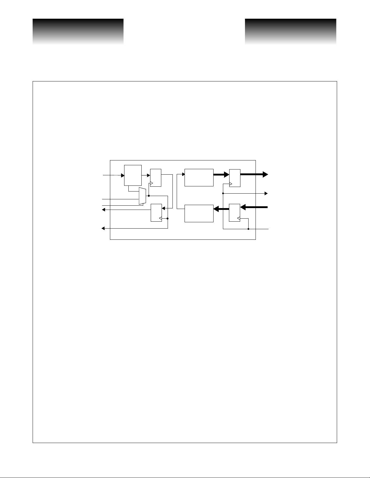
General Description
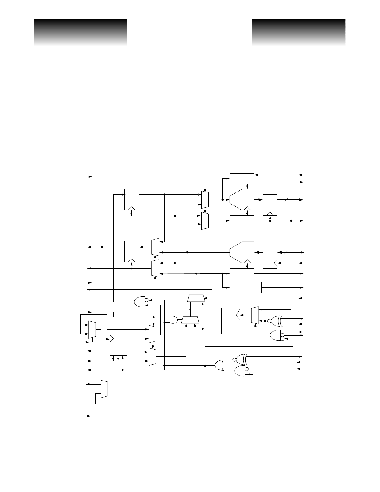
The VSC8113 is an ATM/SONET/SDH compatible transceiver integrating an on-chip Clock Multiplication
Unit (PLL) for the high speed clock as well as a clock and data recovery unit (CRU) with 8 bit serial-to-parallel
and parallel-to-serial data conversion. The PLL clock is used for serialization in the transmit direction (Mux).
The recovered clock is used for deserializatio n in the receive direction (Demux). Th e demultiplexer contains
SONET/SDH frame detection and recovery. The device provides both facility and equipment loopback modes
and two loop timing modes. The part is packa ged in a 100PQFP with integrat ed hea t sp reader fo r opt i mum t her mal performance and reduced cost. The VSC8113 provides an integrated solution for ATM physical layers and
SONET/SDH systems applications.
Functional Description
The VSC8113 is designed to provide a SONET/SDH compliant interface between the high spee d optical
networks and the lower speed User Network Interface devices such as the PM5355 S/UNI-622. The VSC8113
converts 8 bit parallel data at 77.76Mb/s or 19Mb/s to a serial bit stream at 622.08Mb/s or 155.52Mb/s respectively. The device also provides a Facility Loopback function which loops the received high speed data and
clock (optionally recovered on-chip) directly to the high speed transmit outputs. A Clock Multiplier Unit
(CMU) is integrated into the transmit circuit to generate the high speed clock for the serial output data stream
from input reference frequencies of 19.44, 38.88, 51.84 or 77.76 MHz. The CMU can be bypassed with the
received/recovered clock in loop timing mode thus synchronizin g the entire part to a sing le clock. The blo ck
diagram on page 2 shows the major functional blocks associated with the VSC8113.
The receive section provides the serial-to-parallel c onversion, converting the 155.52Mb/s or 622Mb/s bit
stream to an 8 bit parallel o utput at 19.44Mb /s or 77. 76MHz respectively. A Clock Reco v ery Unit (CRU) is integrated into the receive circuit to recover the high speed clock from the received serial data stream. The receive
section provides an Equipment Loopback function which will loop the low speed transmit data and clock back
through the receive section to the 8 bit par allel data bus and clock outputs.The V SC8113 also pr ovides the
option of selecting between either its internal CRU’s recovered clock and data signals or optics containing a
G52154-0, Rev 4.2
3/19/99 741 Calle Plano, Camarillo, CA 93012 • 805/388-3700 • FAX: 805/987-5896
VITESSE SEMICONDUCTOR CORPORATION
Page 1
Page 2
VITESSE
SEMICONDUCTOR CORPORATION
ATM/SONET/SDH 622 Mb/s Transceiver Mux/Demux
with Integrated Clock Generation and Clock Recovery
Data Sheet
VSC8113
CRU clock and data signals. (In this mode the VSC8113 operates just like the VSC8111). The receive section
also contains a SONET/SDH f rame detector cir cuit which is use d to provide frame pluse s during the A1, A2
boundary in the serial to parallel converter . This only occurs when OOF is high. Both internal and external LOS
functions are supported.
VSC8113 Block Diagram
EQULOOP
TXDATAOUT+/-
TXCLKOUT+/-
FACLOOP
CMULOCKDET
DQ
DQ
FRAMER
0
1
0
1
1
0
1
0
01
1:8
DEMUX
Divide-by-8
8:1
MUX
Divide-by-8
Divide-by-3/12
DQ
QD
8
8
OOF
FP
RXOUT[7:0]
RXLSCKOUT
TXIN[7:0]
TXLSCKIN
TXLSCKOUT
RX50MCK
LOOPTIM0
DSBLCRU
1
RXDATAIN+/-
CRUEQLP
CRULOCKDET
RXCLKIN+/-
LOSOUT
CRUREFCLK
CRUREFSEL
0
1
0
CRU
REC-DATA
REC-CLK
Page 2
741 Calle Plano, Camarillo, CA 93012 • 805/388-3700 • FAX: 805/987-5896 3/19/99
10
1
0
0
1
losdet
cmurefclk
CMU
VITESSE SEMICONDUCTOR CORPORATION
1
0
REFCLKP+/REFCLK
LOOPTIM1
EQULOOP
LOSPECL
LOSTTL
LOSDETEN_
G52154-0, Rev 4.2
Page 3
VITESSE
SEMICONDUCTOR CORPORATION
Data Sheet
SC8113
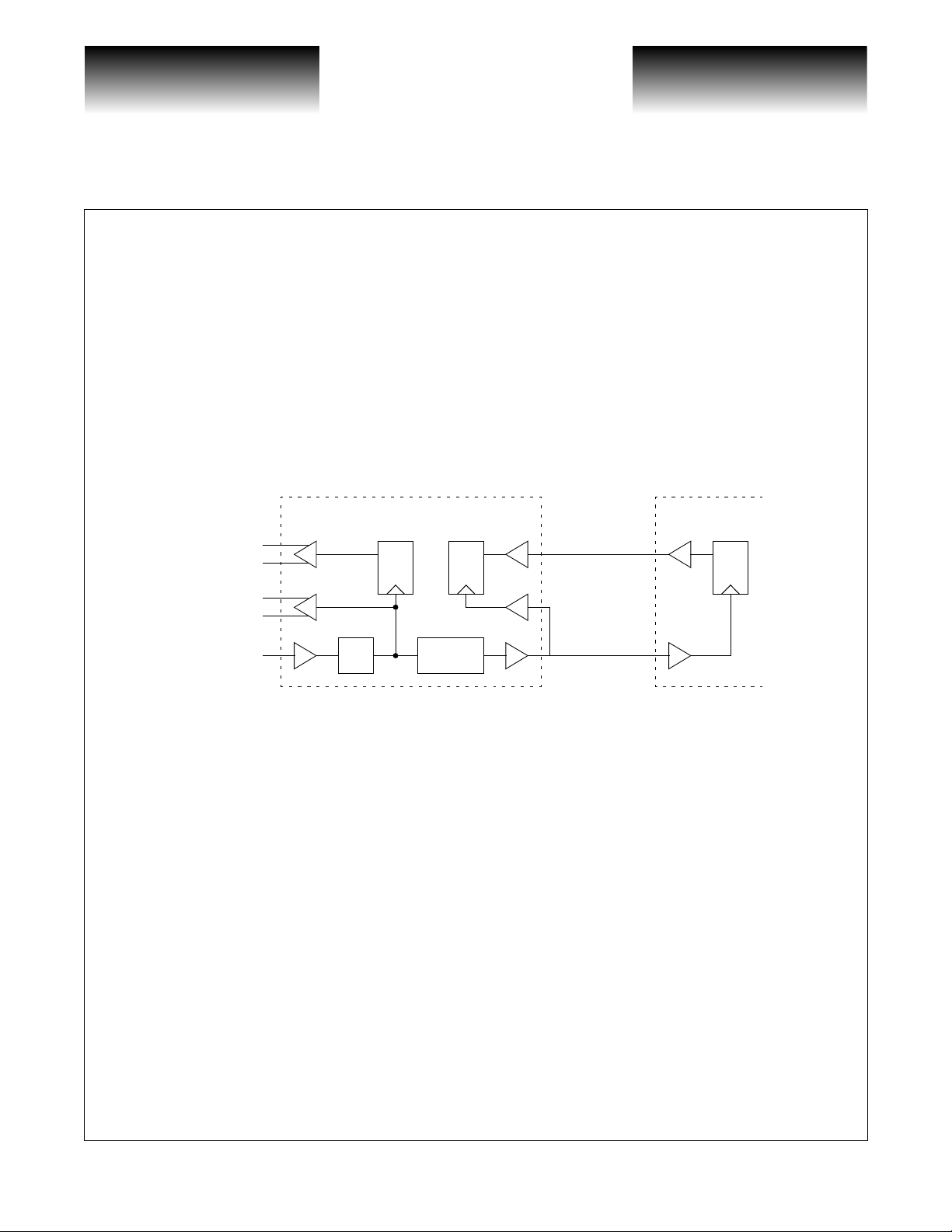
Transmit Section
Byte-wide data is presented to TXIN[7:0] and is clocked into the part on the rising edge of TXLSC KIN.
See Figure 1. The data is then serialized (MSB leading) and presented at the TXDATAOUT+/- pins.
TXDATAOUT is clocked out on the falling edge of TXCLKOUT+. The serial output stream is synchronized to
the CMU generated clock whic h is a phase locked and frequen cy scaled version of the inp ut reference cloc k.
External control inputs B0-B2 and STS-12 select the multiply ratio of the CMU for either STS-3 (155MbS) or
STS-12 (622Mb/s) transmission (see Table 12). A divide-by-8 version of the CMU clock (TXLSCKOUT)
should be used to synchronize the transmit interface of the UNI device to the transmit input registers on the
VSC8113 (see Application Notes, p. 20).
Figure 1: Data and Clock Transmit Block Diagram
TXDATAOUT+
TXDATAOUT-
TXCLKOUT+
TXCLKOUT-
ATM/SONET/SDH 622 Mb/s Transceiver Mux/Demux
with Integrated Clock Generation and Clock Recovery
VSC8113 PM5355
DQDQ
TXIN[7:0]
TXLSCKIN
DQ
REFCLK
Receive Section
High speed Non-Return to Zero (NRZ) serial data at 155Mb/s or 622Mb/s are received by the RXDATAIN
inputs. The CRU recovers the high speed clock from the serial data input. The serial data is converted to bytewide parallel data and presented on RXOUT[7:0] pins. A divide-by-8 version of the high-speed clock
(RXLSCKOUT) should be used to synch r onize t he byte-serial RXOUT[7:0] data with the receive portion of the
UNI device. The on-chip CRU is by-passed by setting the DSBLCRU input high. In this mode, the serial input
data and corresponding clock are received by the RXDATAIN and RXCLKIN inputs respectively. RXDATAIN
is clocked in on the rising edge of RXCLKIN+. See Figure 2.
The receive section also includes frame detection a nd recovery circuitry which detec ts the SONET/SDH
frame, aligns the received serial data on byte boundaries, and initiates a frame pulse on FP coincident with the
byte aligned data. The frame recovery is initiated when OOF is held high which must occur at lea s t 4 byte clock
cycles before the A1A2 boundary. The OOF input control is a level-sensitive signal, and th e VSC8113 will continually perform frame detection and recovery as long as this pin is held high even if 1 or more frames has been
detected. Frame detection and recovery occurs when a series of three A1 bytes followed by three A2 bytes has
been detected. The paralle l outp ut data on R XOUT[7:0] wil l be b yt e alig ned startin g on the thi rd A2 b yte. Wh en
a frame is detected, a single byte clock pe riod long pulse is g enerated o n FP which i s synchronize d with the
byte-aligned third A2 byte on RXOUT[7:0]. The frame detector sends a FP pulse only if OOF is high.
Divide-by-8CMU
TXLSCKOUT
G52154-0, Rev 4.2
3/19/99 741 Calle Plano, Camarillo, CA 93012 • 805/388-3700 • FAX: 805/987-5896
VITESSE SEMICONDUCTOR CORPORATION
Page 3
Page 4
VITESSE
SEMICONDUCTOR CORPORATION
ATM/SONET/SDH 622 Mb/s Transceiver Mux/Demux
with Integrated Clock Generation and Clock Recovery
Data Sheet
VSC8113
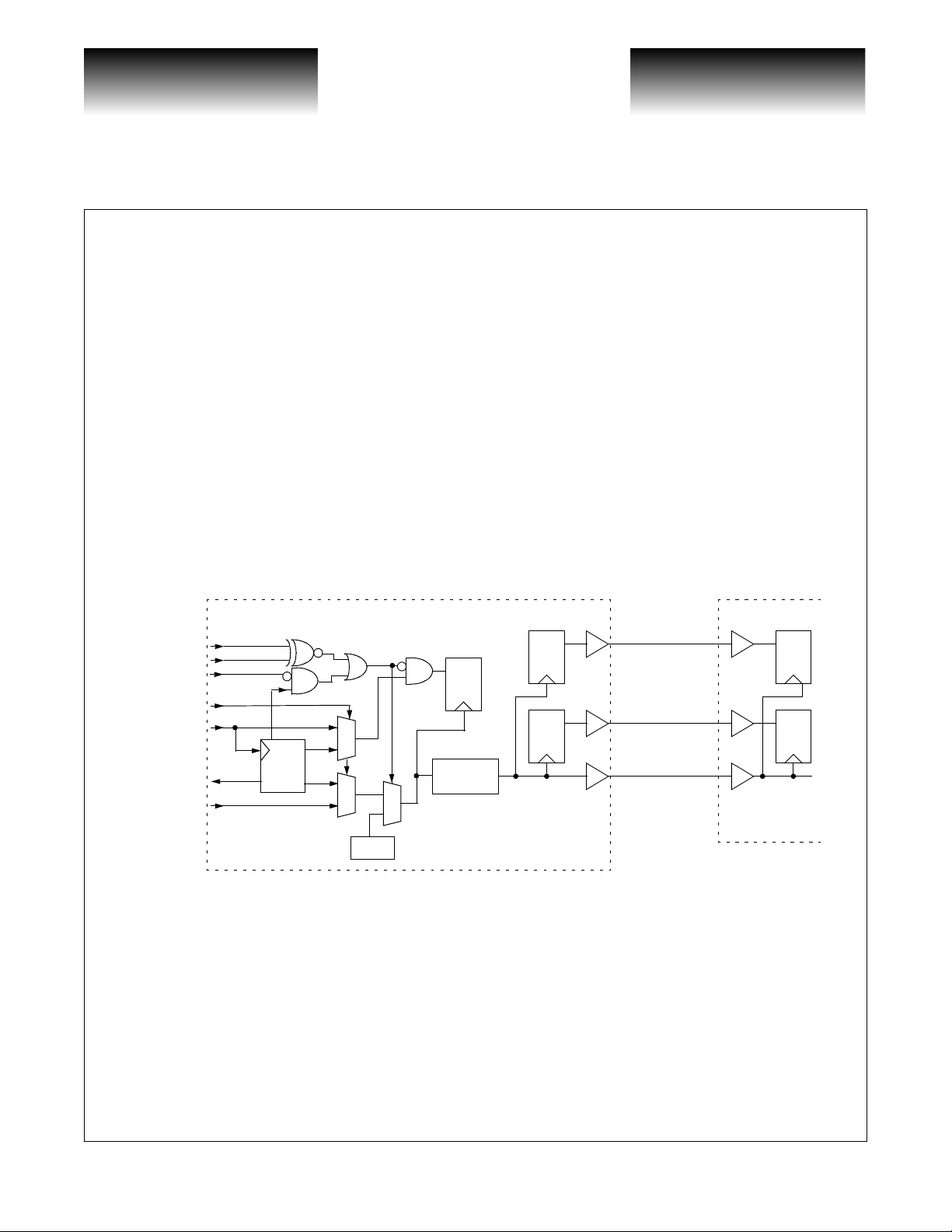
Loss of Signal
The VSC8113 features Loss of Signal (LOS) detection. Loss of Signal is declared if the incoming serial
data stream has no transition continuously for more than 128 bits. During an LOS condition, the VSC 8113
forces the receive data low which is an indication for an y do wnstre am equipment that an optical interfac e fail ure
has occurred. The receive section continues to be clocked by the CRU as it is now locked to the “CRUREFCLK” unless “DSBLCRU” is active in which case it will be clocked by the CMU. This LOS condition will be
removed when the part detects more than 16 transitions in a 128 bit time window. This LOS detection feature
can be disabled by applying a high level to LOSDETEN_ input. The VSC8113 also has a TTL input LOSTTL
and a PECL input LOSPECL to force the part into a Loss of Signal state. Most optics have a PECL output usually called “SD” or “FLAG” indicating a lack of or presence of optical power. Depending on the optics manufactured this signal is either active high or active low. The LOSTTL and LOSPECL inputs are XNOR’d to
generate an internal LOS control signal. See Figure 2. The optics “SD” output should be connected to
LOSPECL. The LOSTTL input should be tied low if the optics “SD” output is active high. If it’s active low tie
LOSTTL high. The inverse is true if the optics use “FLAG” for loss of signal.
Figure 2: Data and Clock Receive Block Diagram
VSC8113
PM5355
LOSPECL
LOSTTL
LOSDETEN_
DSBLCRU
RXDATAIN+/-
CRULOCKDET
RXCLKIN+/-
CRU
DQ
DQ
1
0
0
0
1
1
CMU
Divide-by-8
DQ
RXOUT[7:0]
FP
RXLSCKOUT
DQ
DQ
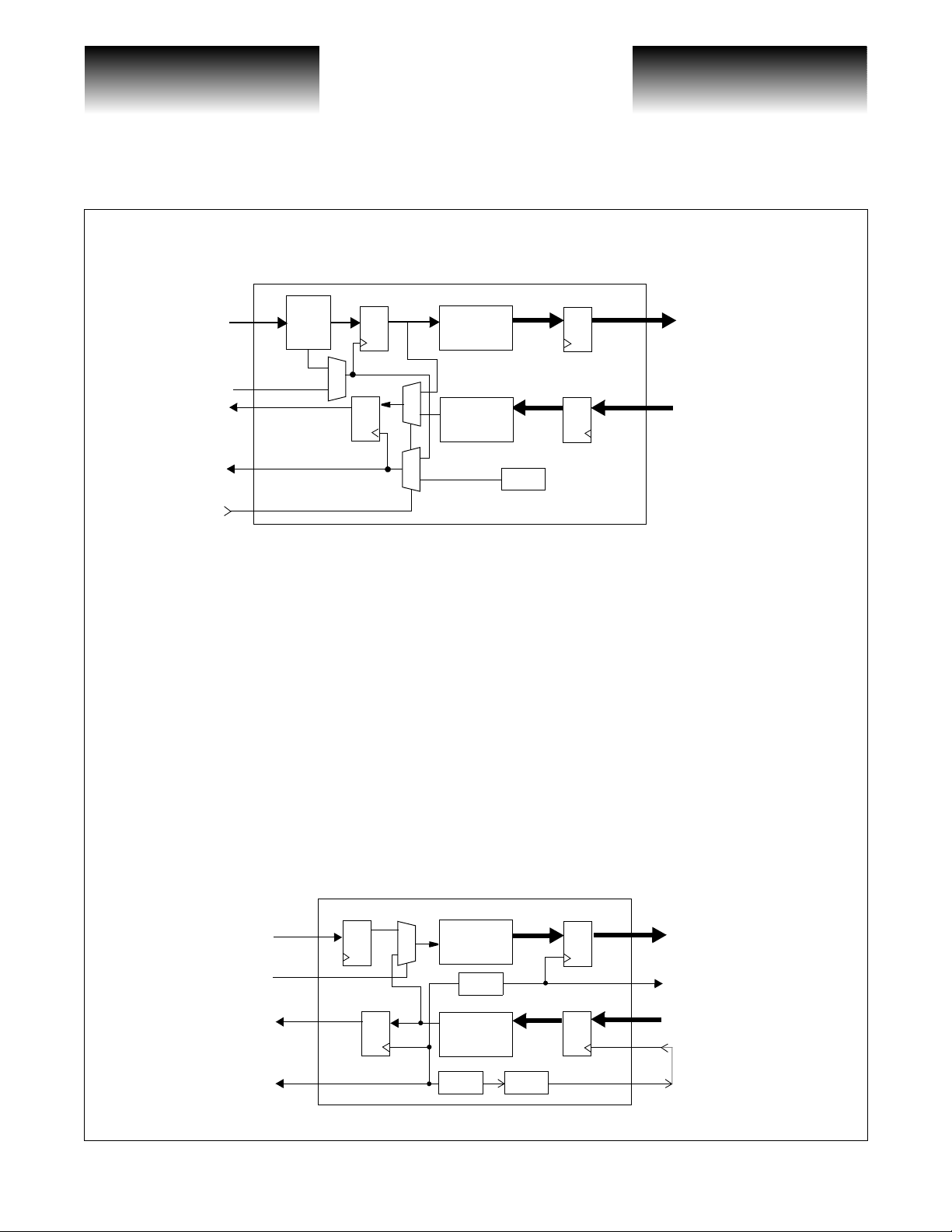
Facility Loopback
The Facility Loopback function is controlled by the FACLOOP signal. When the FACLOOP signal is set
high, the Facility Loopback mode is activated and the high speed serial receive data (RXDATAIN) is presented
at the high speed transmit output (TXDATAOUT). See Figure 3. In addition, the high speed received/recovered
clock is selected and p resented at the high speed tra nsmit clock outp ut (TXCLKOUT). In Facility Loopback
mode the high speed recei v e dat a (RXDATAIN) is also co nverted to parall el data and presented at the low speed
receive data output pins (RXOUT[7:0]). The receive clock (RXCLKIN) is also divided down and presented at
the low speed clock output (RXLSCKOUT).
Page 4
741 Calle Plano, Camarillo, CA 93012 • 805/388-3700 • FAX: 805/987-5896 3/19/99
VITESSE SEMICONDUCTOR CORPORATION
G52154-0, Rev 4.2
Page 5
VITESSE
SEMICONDUCTOR CORPORATION
Data Sheet
SC8113
ATM/SONET/SDH 622 Mb/s Transceiver Mux/Demux
with Integrated Clock Generation and Clock Recovery
Figure 3: Facility Loopback Data Path
RXDATAIN
RXCLKIN
TXDATAOUT
TXCLKOUT
FACLOOP
Recovered
Clock
CRU
Q
0
1
Q
1
D
0
1
0
1:8
Serial to
Parallel
Parallel to
Serial
PLL
D
Q
Q
D
RXOUT[7:0]
TXIN[7:0]8:1
D
Equipment Loopback
The Equipment Loopback function is controlled by the EQULOOP signal. When the EQULOOP signal is
set high, the Equipment Loopback mode is activated and the high speed transmit data generated from the parallel to serial conversion of the low speed data (TXIN[7:0]) is selected and converted back to parallel data in the
receiver section and presented at the low speed parallel outputs (RXOUT[7:0]). See Figure 4. The internally
generated 155/622MHz clock i s used t o g enerate t he low speed receive clock output (RXLSCKOUT). In Equipment Loopback mode the transmit data (TXIN[7:0]) is serialized and presented at the high speed output
(TXDATAOUT) along with the high speed transmit clock (TXCLKOUT) which is generated by the on-chip
clock multiplier unit.
CRU Equipment Loopback
Exactly the same as equipment loopback, the point where the transmit data is looped back is moved all the
way back to the high speed I/O. When the CRUEQLP signal is set high, transmit data is looped back to the
CRU, replacing RXDATAIN±
Figure 4: Equipment Loopback Data Path
D
RXDATAIN
EQULOOP
TXDATAOUT
TXCLKOUT
G52154-0, Rev 4.2
Q
0
1
Q
D
VITESSE SEMICONDUCTOR CORPORATION
1:8
Serial to
Parallel
÷ 8
8:1
Parallel to
Serial
PLL ÷ 8
3/19/99 741 Calle Plano, Camarillo, CA 93012 • 805/388-3700 • FAX: 805/987-5896
D
Q
Q
D
RXOUT[7:0]
RXLSCKOUT
TXIN[7:0]
TXLSCKIN
TXLSCKOUT
Page 5
Page 6
VITESSE
SEMICONDUCTOR CORPORATION
ATM/SONET/SDH 622 Mb/s Transceiver Mux/Demux
with Integrated Clock Generation and Clock Recovery
Data Sheet
VSC8113
Split Loopback
Equipment and facility loopback modes can be enabled simultaneously. In this case, high-speed serial data
received (RXDATAIN) and received/recovered clock are mux’d through to the high-speed serial outputs
(TXDATAOUT) and (TXCLKOUT). The low-speed transmit byte wide bus(TXIN[7:0]) and (TXLSCKIN) are
mux’d into the low-speed byte wide receive output bus (RXOUT[7:0]) and (RXLSCKOUT). See Figure 5.
Figure 5: Split Loopback Datapath
D
RXDATAIN
RXCLKIN
DSBLCRU
TXDATAOUT
TXCLKOUT
Recovered
Clock
CRU
Q
0
1
Q
D
1:8
Serial to
Parallel
8:1
Parallel to
Serial
D
Q
Q
D
RXOUT[7:0]
RXLSCKOUT
TXIN[[7:0]
TXLSCKIN
Loop Timing
LOOPTIM0 mode bypasses the CMU when the LOOPTIM0 input is asserted high. In this mode the CMU
is bypassed by using the receive clock (RXCLKIN), and the entire part is synchronously clocked from a single
external source.
LOOPTIM1 mode bypasses the REFCLK input and uses the divide-by-8 version of the receive clock as the
reference input to the CMU. This mode is selected by asserting the LOOPTIM1 input high. The part is forced
out of this mode if it is in the Loss of Signal state or in Equipment Loopback to prevent the CMU from feeding
its own clock back.
Clock Synthesis
The VSC8113 uses an integrated phase-locked loop (PLL) for c lock synthesis of the 622MHz hig h speed
clock used for serialization in the transmitter section. The PLL is comprised of a phase-frequency detector
(PFD), an integrating operation amplifier and a voltage controlled oscillator (VCO) configured in classic feedback system. The PFD compa res the s elected divided down versio n of the 622M Hz VCO (select pi ns B0-B2
select divide-b y ra tios of 8, 12 , 16 a nd 32, see Table 12) and the reference clock. The int egrat or pro vi des a transfer function betw een inp ut phase e rror and out put v olta ge contr ol. T he VCO port ion o f the PLL is a v olt age controlled ring-oscillator with a center frequency of 622MHz.
The reactive elements of the integrator are located off-chip and are connected to the feedback loop of the
amplifier through the CP1, CP2, CN1 and CN2 p ins. The configuration of thes e external surface moun ted
capacitors is shown in Figure 6. Table 1 shows the recommended external capacitor values for the configurable
reference frequencies.
Page 6
741 Calle Plano, Camarillo, CA 93012 • 805/388-3700 • FAX: 805/987-5896 3/19/99
VITESSE SEMICONDUCTOR CORPORATION
G52154-0, Rev 4.2
Page 7
VITESSE
SEMICONDUCTOR CORPORATION
Data Sheet
SC8113
Good analog design practices should be applied to the board design for these external components. Tightly
controlled analog ground and power planes should be provided for the PLL portion of the circuitry. The dedicated PLL power (VDDANA) and ground (VSSANA) pins should have quiet supply planes to minimize jitter
generation within the clock synthesis unit. This is accomplished by either using a ferrite bead or a C-L-C choke
(π filter) on the (VDDANA) power pins. Note: Vitesse recommends a (π filter) C-L-C choke over using a ferrite
bead. All ground planes should be tied together using multiple vias.
The VSC8113 features a lock detect function for the CMU, called “CMULOCKDET”. It generates low
going pulses when the CMU is locked to the incoming REFCLK. This is accomplished by comparing the phase
of the synthesized clock to the reference clock. If the “CMULOCKDET” output remains high for >
CMU is locked.
Reference Clocks
To improve jitter performance and to provide flexibility, an additional differential PECL reference clock
input is provided. This reference clock is internally XNOR’d with a TTL reference clock input to generate the
reference for the CMU. Vitesse reco mmends u s ing t he di fferential PECL i nput and tieing the unused TTL r efer ence clock low. If the TTL reference clock is used the positive side of the differential PECL reference clock
“REFCLKP+” should be tied to ground. “REFCLKP+/-” are internally biased with on-chip resistors to 1.65
volts, see figure 14 for schematic of internal biasing of differential I/O’s.
The CRU has the option of either using the CMU’s reference clock or its own independent reference clock
“CRUREFCLK”. If the CMU reference clock is used, it must be 78MHz. This is accomplished with the control
signal “CRUREFSEL”. The “CRUREFCLK” should be used if the system is being operated in either a regeneration or looptiming mode. In either of these modes the quality of the “CRUREFCLK” is not a concern, thus it
can be driven by a simple 77.76MHz crystal, the key is its’ independent of the CMU’s reference clock.
ATM/SONET/SDH 622 Mb/s Transceiver Mux/Demux
with Integrated Clock Generation and Clock Recovery
10µs, the
Table 1: Recommended External Capacitor Values
Reference
Frequency
[MHz]
19.44 32 0.1 0.1 X7R 0603/0803 +/-10%
38.88 16 0.1 0.1 X7R 0603/0803 +/-10%
51.84 12 0.1 0.1 X7R 0603/0803 +/-10%
77.76 8 0.1 0.1 X7R 0603/0803 +/-10%
G52154-0, Rev 4.2
3/19/99 741 Calle Plano, Camarillo, CA 93012 • 805/388-3700 • FAX: 805/987-5896
Divide Ratio CP CN Type Size Tol.
VITESSE SEMICONDUCTOR CORPORATION
Page 7
Page 8
VITESSE
SEMICONDUCTOR CORPORATION
ATM/SONET/SDH 622 Mb/s Transceiver Mux/Demux
with Integrated Clock Generation and Clock Recovery
Figure 6: External Integrator Capacitor
CP = 0.1 µF
CP1
+
-
CN1 CN2
Clock Recovery
The fully monolithic Clock Recovery Unit (CRU) consists of a Phase Detector, a Frequency Detector, a
Loop Filter and a Voltage Controlled Oscillator (VCO). The phase detector compares the phase information of
the incoming data with the recovered clock. The frequency detector compares the frequency component of the
data input with the recovered clock to provide the pull in energy during lock acquisition. The LoopFilter integrates the phase information from the phase and frequency detectors and provides the control voltage to the
VCO.
The CRU provides a lock detect function. If the frequencies of the serial data stream and the CRU’s recovered clock are different, a data bit in the seri al data stream wil l occasional ly be dropped. If the Fre quenc y Detector does not detect this condition in a moving 1.5 µs window, the CRULOCKDET output is asserted to signal
that the CRU is frequency locked to the serial data stream. This output is forced low if it detects that a data bit is
dropped or if the recovered clock frequency drifts more than 5% from the CMU’s output frequency.
CP2
CN = 0.1 µF
Data Sheet
VSC8113
Page 8
741 Calle Plano, Camarillo, CA 93012 • 805/388-3700 • FAX: 805/987-5896 3/19/99
VITESSE SEMICONDUCTOR CORPORATION
G52154-0, Rev 4.2
Page 9

VITESSE
SEMICONDUCTOR CORPORATION
Data Sheet
SC8113
Jitter Tolerance
Jitter Tolerance is the ability of the Clock Recovery Unit to track timing variation in the received data
stream. The bellcore and ITU specifications allow the received optical data to conta in jitter. The amount that
must be tolerated is a functio n of the f requenc y of t he jitter. At high frequencies the specifications do not r equire
the CRU to tolerate large amounts, wh er eas at l ow frequen cies many unit i nt e rvals (bit t i me s) of jitter ha ve to be
tolerated. The CRU is designed to tolerate th is jitter with margin over the specification limits, see Fi gure 7. The
CRU obtains and maintains lock ba sed on the data t ransition informa tion. W hen t here is no tra nsition on the
data stream, the recovered clock frequency can drift. The VSC811 3 can maintain lock over 100 bits of no
switching on data stream.
ATM/SONET/SDH 622 Mb/s Transceiver Mux/Demux
with Integrated Clock Generation and Clock Recovery
Figure 7: Jitter Tolerance
JITTER(UI P-P)
150
Bellcore Requirement
60
VSC8113 Guaranteed
Jitter Tolerance
15
1.5
0.15
10 30 300 25K 250K
6
0.6
2.5M
JITTER FREQ(HZ)
G52154-0, Rev 4.2
3/19/99 741 Calle Plano, Camarillo, CA 93012 • 805/388-3700 • FAX: 805/987-5896
VITESSE SEMICONDUCTOR CORPORATION
Page 9
Page 10

VITESSE
SEMICONDUCTOR CORPORATION
ATM/SONET/SDH 622 Mb/s Transceiver Mux/Demux
with Integrated Clock Generation and Clock Recovery
AC Timing Characteristics
Figure 8: Receive High Speed Data Input Timing Diagram
T
RXCLK
RXCLKIN+
RXCLKIN-
RXDATAIN+
RXDATAIN-
Table 2: Receive High Speed Data Input Timing T ab le
Parameter Description Min Typ Max Units
T
RXCLK
T
RXSU
T
RXH
Receive clock period - 1.608 - ns
Serial data setup time with respect to RXCLKIN 250 - - ps
Serial data hold time with respect to RXCLKIN 250 - - ps
T
RXSU
T
RXH
(STS-12 Operation)
Data Sheet
VSC8113
Table 3: Receive High Speed Data Input Timing T ab le
(STS-3 Operation)
Parameter Description Min Typ Max Units
T
RXCLK
T
RXSU
T
RXH
Receive clock period - 6.43 - ns
Serial data setup time with respect to RXCLKIN 1.5 - - ns
Serial data hold time with respect to RXCLKIN 1.5 - - ns
Figure 9: Transmit Data Input Timing Diagram
T
PROP
TXLSCKOUT
T
CLKIN
TXLSCKIN
T
INH
TXIN [7:0]
T
INSU
Page 10
741 Calle Plano, Camarillo, CA 93012 • 805/388-3700 • FAX: 805/987-5896 3/19/99
VITESSE SEMICONDUCTOR CORPORATION
G52154-0, Rev 4.2
Page 11

VITESSE
SEMICONDUCTOR CORPORATION
Data Sheet
SC8113
Table 4: Transmit Data Input Timing Table
ATM/SONET/SDH 622 Mb/s Transceiver Mux/Demux
with Integrated Clock Generation and Clock Recovery
(STS-12 Operation)
Parameter Description Min Typ Max Units
T
CLKIN
T
INSU
T
INH
T
PROP
Table 5: Transmit Data Input Timing Table
Transmit data input byte clock period - 12.86 - ns
Transmit data setup time with respect to TXLSCKIN 1.0 - - ns
Transmit data hold time with respect to TXLSCKIN 1.0 - - ns
Maximum allowable pro pagation delay for connecting
TXLSCKOUT to TXLSCKIN
--3.5ns
(STS-3 Operation)
Parameter Description Min Typ Max Units
T
CLKIN
T
INSU
T
INH
T
PROP
Note: Duty cycle for TXLSCKOUT is 50% +/- 10% worst case
Transmit data input byte clock period - 51.44 - ns
Transmit data setup time with respect to TXLSCKIN 1.0 - - ns
Transmit data hold time with respect to TXLSCKIN 1.0 - - ns
Maximum allowable propagation delay for connecting
TXLSCKOUT to TXLSCKIN
--30ns
Figure 10: Receive Data Output Timing Diagram
T
RXCLKIN+
RXCLKIN-
RXLSCKOUT
RXOUT [7:0]
Table 6: Receive Data Output Timing Table
RXCLKIN
T
RXLSCK
A1 A2 A2 A2 A2
(STS-12 Operation)
Parameter Description Min Typ Max Units
T
RXCLKIN
T
RXLSCK
T
RXVALID
T
PW
Receive clock period - 1.608 - ns
Receive data output byte clock period - 12 .86 - ns
Time data on RXOUT [7:0] and FP is valid before and
after the rising edge of RXLSCKOUT
Pulse width of fram e detection pulse FP - 12.86 - ns
4.0 - - ns
G52154-0, Rev 4.2
3/19/99 741 Calle Plano, Camarillo, CA 93012 • 805/388-3700 • FAX: 805/987-5896
VITESSE SEMICONDUCTOR CORPORATION
Page 11
Page 12

VITESSE
SEMICONDUCTOR CORPORATION
ATM/SONET/SDH 622 Mb/s Transceiver Mux/Demux
with Integrated Clock Generation and Clock Recovery
Table 7: Receive Data Output Timing Table
Parameter Description Min Typ Max Units
T
RXCLKIN
T
RXLSCKT
T
RXVALID
T
PW
Receive clock period - 6.43 - ns
Receive data output byte clock period - 51 .44 - ns
Time data on RXOUT [7:0] and FP is valid before and
after the rising edge of RXLSCKOUT
Pulse width of fram e detection pulse FP - 51.44 - ns
Figure 11: Transmit High Speed Data Timing Diagram
TXCLKOUT-
TXCLKOUT+
TXDATAOUT+
TXDATAOUT-
(STS-3 Operation)
T
TXCLK
T
T
SKEW
SKEW
22 - - ns
Data Sheet
VSC8113
Table 8: Transmit High Speed Data Timing Table
(STS-12 Operation)
Parameter Description Min Typ Max Units
T
TXCLK
T
SKEW
Table 9: Transmit High Speed Data Timing Table
Transmit clock period - 1.608 - ns
Skew between the f allin g e dg e of TXCLKOUT+ and
valid data on TXDATAOUT
--250ps
(STS-3 Operation)
Parameter Description Min Typ Max Units
T
TXCLK
T
SKEW
Transmit clock period - 6.43 - ns
Skew between the f allin g e dg e of TXCLKOUT+ and
valid data on TXDATAOUT
--250ps
Page 12
741 Calle Plano, Camarillo, CA 93012 • 805/388-3700 • FAX: 805/987-5896 3/19/99
VITESSE SEMICONDUCTOR CORPORATION
G52154-0, Rev 4.2
Page 13

VITESSE
SEMICONDUCTOR CORPORATION
Data Sheet
SC8113
ATM/SONET/SDH 622 Mb/s Transceiver Mux/Demux
with Integrated Clock Generation and Clock Recovery
Data Latency
The VSC8113 contains several operating modes, each of which exercise different logic paths through the
part. Table 10 bounds the data latency through each path with an associated clock signal.
Table 10: Data Latency
Circuit Mode Description
Transmit Data TXIN [7:0] to MSB at TXDATAOUT TXCLKOUT 4-13
Receive MSB at RXDATAIN to data on RXOUT [7:0] RXCLKIN 25-35
Equipment
Loopback
Facilities
Loopback
Byte data TXIN [7:0] to byte data on RXOUT [7:0] TXCLKOUT 27-3 5
MSB at RXDATAIN to MSB at TXDATAOUT RXCLKIN 2-4
Reference
Clock Recovery Unit
Table 11: Reference Frequency for the CRU
Clock
Range of Clock
cycles
CRUREFSEL
11XXX77.76 ± 500ppm 622.0 8
1 0 X X X 77.76 ± 500ppm 155.52
0 Uses CMU’s Reference Clock (See Table 12 below)
STS12 B2 B1 B0
CRUREFCLK
Frequency
[MHz]
Clock Multiplier Unit
Table 12: Reference Frequency Selection and Output Frequency Control
Reference
STS12 B2 B1 B0
111019.44622.08
101038.88622.08
100151.84622.08
100077.76622.08
011019.44155.52
001038.88155.52
000151.84155.52
000077.76155.52
Frequency
[MHz]
Output
Frequency
[MHz]
Output
Frequency
[MHz]
G52154-0, Rev 4.2
3/19/99 741 Calle Plano, Camarillo, CA 93012 • 805/388-3700 • FAX: 805/987-5896
VITESSE SEMICONDUCTOR CORPORATION
Page 13
Page 14

VITESSE
SEMICONDUCTOR CORPORATION
ATM/SONET/SDH 622 Mb/s Transceiver Mux/Demux
with Integrated Clock Generation and Clock Recovery
Table 13: Clock Multiplier Unit Performance
Name Description Min Typ Max Units
RCd Reference clock duty cycle 40 60 %
RCj Reference clock jitter (RMS) @ 77.76 MHz ref
RCj Reference clock jitter (RMS) @ 51.84 MHz ref
RCj Reference clock jitter (RMS) @ 38.88 MHz ref
RCj Reference clock jitter (RMS) @ 19.44 MHz ref
RC
f
OCj Output clock jitter (RMS) @ 77.76 MHz ref
OCj Output clock jitter (RMS) @ 51.84 MHz ref
OCj Output clock jitter (RMS) @ 38.88 MHz ref
OCj Output clock jitter (RMS) @ 19.44 MHz ref
OCf
range
OCd Output clock duty cycle 40 60 %
(1) These Reference Clock Jitter limits are r e quired for the outputs to meet SONET system level jitter requirem ent s
(< 10 mUIrms)
(2) Needed to meet SONET output frequency stability requirements
(3) Measured
Reference clock frequency tolerance
Output frequency 620 624 MHz
(2)
(1)
(1)
(1)
(1)
-20 +20 ppm
(3)
(3)
(3)
(3)
Data Sheet
VSC8113
13 ps
12 ps
9ps
5ps
8ps
10 ps
13 ps
15 ps
Note: Jitter specification is defined utilizing a 12KHz - 5MHz LP-HP single pole filter.
AC Characteristics
Table 14: PECL and TTL Outputs
Parameters Description Min Typ Max Units Conditions
T
R,TTL
T
F,TTL
T
R,PECL
T
F,PECL
TTL Output Rise Time
TTL Output Fall Time
PECL Output Rise Time
PECL Output Fall Time
—2—ns
—1.5—ns
—350— ps
—350— ps
10-90%
10-90%
20-80%
20-80%
Page 14
741 Calle Plano, Camarillo, CA 93012 • 805/388-3700 • FAX: 805/987-5896 3/19/99
VITESSE SEMICONDUCTOR CORPORATION
G52154-0, Rev 4.2
Page 15

VITESSE
SEMICONDUCTOR CORPORATION
Data Sheet
SC8113
ATM/SONET/SDH 622 Mb/s Transceiver Mux/Demux
with Integrated Clock Generation and Clock Recovery
DC Characteristics
Table 15: PECL and TTL Inputs and Outputs
Parameters Description Min Typ Max Units Conditions
∆V
∆V
V
V
V
OCM
OUT75
OUT50
V
V
∆V
V
ICM
V
V
V
V
I
IH
I
OH
OL
IH
IL
OH
OL
IH
IL
IL
IN
Output HIGH
voltage (PECL)
Output LOW
voltage (PECL)
O/P Common
Mode Range
(PECL)
Differential
Output Voltage
(PECL)
Differential
Output Voltage
(PECL)
Input HIGH
voltage (PECL)
Input LOW
voltage (PECL)
Differential Input
Voltage (PECL)
I/P Common
Mode Range
(PECL)
Output HIGH
voltage (TTL)
Output LOW
voltage (TTL)
Input HIGH
voltage (TTL)
Input LOW
voltage (TTL)
Input HIGH
current (TTL)
Input LOW
current (TTL)
——V
0.7 —— V
1.1 —V
600 —1300mV
600 —1300mV
V
– 0.9V — V
DDP
0—V
400 — 1600 mV
1.5 – ∆V
/2 — V
IN
2.4 —— V
—— 0.5 V
2.0 — 5.5 V
0 —0.8 V
—50 500 µA
—— -500 µA
– 0.9V V
DDP
– 1.3V V
DDP
– 0.3V V
DDP
– 1.72V V
DDP
– 1.0 – ∆V
DDP
/2 V
IN
—
—
—
75Ω to V
50Ω to V
For single ended
For single ended
—
—
IOH = -1.0 mA
IOL = +1.0 mA
—
—
2.0V< VIN < 5.5V,
Typical@2.4V
-0.5V < VIN < 0.8V
DDP
DDP
– 2.0 V
– 2.0 V
G52154-0, Rev 4.2
3/19/99 741 Calle Plano, Camarillo, CA 93012 • 805/388-3700 • FAX: 805/987-5896
VITESSE SEMICONDUCTOR CORPORATION
Page 15
Page 16

VITESSE
SEMICONDUCTOR CORPORATION
ATM/SONET/SDH 622 Mb/s Transceiver Mux/Demux
with Integrated Clock Generation and Clock Recovery
Data Sheet
VSC8113
Power Dissipation
Table 16: Power Supply Currents
Parameter Description (Max) Units
I
DD
P
D
Absolute Maximum Ratings
Power Supply Voltage (VDD) Potential to GND.................................................................................-0.5V to +4V
PECL I/O Supply Voltage (V
DC Input Voltage (PECL inputs).......................................................................................... -0.5V to V
DC Input Voltage (TTL inputs).........................................................................................................-0.5V to 5.5V
DC Output Voltage (TTL Outputs)........................................................................................ -0.5V to V
Output Current (TTL Outputs)................................................................................................................. +/-50mA
Output Current (PECL Outputs)................................................................................................................+/-50mA
Case Temperature Under Bias.........................................................................................................-55
Storage Temperature.....................................................................................................................-65
Maximum Input ESD (Human Body Model).............................................................................................. 1500 V
Power supply current from V
Power dissipation (worst case) 1.6 W
DD
480 mA
(1)
) Potential to GND..........................................................................-0.5V to +6V
DDP
DDP
DD
o
to +125oC
o
C to +150oC
+0.5V
+ 0.5V
Note: Caution: Stresses listed under “Absolute Maximum Ratings” may be applied to devices one at a time without causing
permanent damage. Functionality at or exceeding the values listed is not implied. Exposure to these values for extended
periods may affect device reliability.
Recommended Operating Conditions
Power Supply Voltage (VDD).................................................................................................................+3.3V %
PECL I/O Supply Voltage (V
Commercial Operating Temperature Range..................................................................... 0
Extended Operating Temperature Range...................0
Industrial Operating Temperature Range ......................................................................-40
).......................................................................................... +3.3V or +5.0V %
DDP
o
to 85oC ambient equivalent to 0o ambient to 115oC case
o
ambient to 70oC case
o
ambient to 85oC case
5±
5±
Page 16
741 Calle Plano, Camarillo, CA 93012 • 805/388-3700 • FAX: 805/987-5896 3/19/99
VITESSE SEMICONDUCTOR CORPORATION
G52154-0, Rev 4.2
Page 17

VITESSE
SEMICONDUCTOR CORPORATION
Data Sheet
SC8113
ATM/SONET/SDH 622 Mb/s Transceiver Mux/Demux
with Integrated Clock Generation and Clock Recovery
Package Pin Description
Table 17: Pin Definitions
Signal Pin I/O Level Pin Description
FACLOOP 1 I TTL
VDD 2 +3.3V +3.3V Power Supply
CRUEQLP 3 I TTL Loops TXDATAOUT to the CRU replacing RXDATAIN+/RESET 4 I TTL Resets frame detection, dividers, controls; active high
LOOPTIM0 5 I TTL Enable loop timing operation; active HIGH
B0 6 I TTL Reference clock select, refer to table 12
B1 7 I TTL Reference clock select, refer to table 12
B2 8 I TTL Reference clock select, refer to table 12
VDDP 9 +3.3/+5V +3.3V or +5V Power Supply for PECL I/Os
TXDATAOUT+ 10 O PECL Transmit output, high speed differential data +
TXDATAOUT- 11 O PECL Transmit output, high speed differential data VSS 12 GND Ground
TXCLKOUT+ 13 O PECL Transmit high speed clock differential output+
TXCLKOUT- 14 O PECL Transmit high speed clock differential outputVDDP 15 +3.3/+5V +3.3V or +5V Power Supply for PECL I/Os
N/C 16 No connection
LOSDETEN_ 17 I TTL Enables internal LOS detection (active low).
VSS 18 GND Ground
RXCLKIN+ 19 I PECL Receive high speed differential clock input+
RXCLKIN- 20 I PECL Receive high speed differential clock inputVDDP 21 +3.3/+5V +3.3V or +5V Power Supply for PECL I/Os
OOF 22 I TTL Out Of Frame; Frame detection initiated with high level
DSBLCRU 23 I TTL Disable on-chip clock reco very unit; activ e high
RXDATAIN+ 24 I PECL Receive high speed differential data input+
RXDATAIN- 25 I PECL Receive high speed differential data input NC 26 No conn ection
NC 27 No conn ection
VDD 28 +3.3V +3.3V Power Supply
REFCLKP+ 29 I PECL PECL reference clock input+
REFCLKP- 30 I PECL PECL reference clock input-
Facility loopback, loops high speed receive data and clock
directly to transmit outputs.
G52154-0, Rev 4.2
3/19/99 741 Calle Plano, Camarillo, CA 93012 • 805/388-3700 • FAX: 805/987-5896
VITESSE SEMICONDUCTOR CORPORATION
Page 17
Page 18

VITESSE
SEMICONDUCTOR CORPORATION
ATM/SONET/SDH 622 Mb/s Transceiver Mux/Demux
with Integrated Clock Generation and Clock Recovery
Table 17: Pin Definitions
Signal Pin I/O Level Pin Description
VDD 31 +3.3V +3.3V Power Supply
N/C 32 No connection
RX50MCK 3 3 O TTL
VSS 34 GND Ground
RXOUT0 35 O TTL Receive output data bit0
RXOUT1 36 O TTL Receive output data bit1
VSS 37 GND Ground
RXOUT2 38 O TTL Receive output data bit2
RXOUT3 39 O TTL Receive output data bit3
VSS 40 GND Ground
RXOUT4 41 O TTL Receive output data bit4
RXOUT5 42 O TTL Receive output data bit5
VSS 43 GND Ground
RXOUT6 44 O TTL Receive output data bit6
RXOUT7 45 O TTL Receive output data bit7
VSS 46 GND Ground
RXLSCKOUT 47 O TTL Receive byte clock output
FP 48 O TTL Frame detection pulse
VDD 49 +3.3V +3.3V Power Supply
LOSOUT 50 O TTL Loss of Signal alarm indicator
CRUREFCLK 51 I TTL Optional external CRU reference clock @77.76MHz
LOSTTL 52 I TTL Loss of Signal Control - TTL input
LOSPECL 53 I PECL Loss of Signal Contr ol- Single ended PECL input
VDD 54 +3.3V +3.3V Power Supply
VSS 55 GND Ground
REFCLK 56 I TTL Reference clock input, refer to table 12
LOOPTIM1 57 I TTL Enable loop timing operation; active HIGH
VDD 58 +3.3V +3.3V Power Supply
VSSA 59 GND Analog Ground (CMU)
VSSA 60 GND Analog Ground (CMU)
N/C 61 No connection
VDDA 62 +3.3V Analog Power Supply (CMU)
CP1 63 Analog CMU external capacitor (see Figure 6, and Table 1)
Constant 51.84MHz ref clock output, derived from the CMU
Data Sheet
VSC8113
Page 18
741 Calle Plano, Camarillo, CA 93012 • 805/388-3700 • FAX: 805/987-5896 3/19/99
VITESSE SEMICONDUCTOR CORPORATION
G52154-0, Rev 4.2
Page 19

VITESSE
SEMICONDUCTOR CORPORATION
Data Sheet
SC8113
Table 17: Pin Definitions
Signal Pin I/O Level Pin Description
CN1 64 Analog CMU external capacitor (see Figure 6, and Table 1)
CN2 65 Analog CMU external capacitor (see Figure 6, and Table 1)
CP2 66 Analog CMU external capacitor (see Figure 6, and Table 1)
VDDA 67 +3.3V Analog Power Supply (CMU)
VDDA 68 +3.3V Analog Power Supply (CRU)
VDDA 69 +3.3V Analog Power Supply (CRU)
VSSA 70 GND Analog Ground (CRU)
VSSA 71 GND Analog Grou nd (CRU)
VSS 72 GND Ground
N/C 7 3 No connection
CRULOCKDET 74 O TTL Lock Detect indicator for clock recovery unit
VSS 75 GND Ground
VDD 76 +3.3V +3.3V Power Supply
N/C 7 7 No connection
N/C 7 8 No connection
N/C 7 9 No connection
CMULOCKDET 80 O TTL Lock Detect indicator for clock synthesis unit
VDD 81 +3.3V +3.3V Power Supply
TXLSCKOUT 82 O TTL Transmit byte clock out
TXLSCKIN 83 I TTL Transmit byte clock in
VSS 84 GND Ground
TXIN7 85 I TTL Transmit input data bit7
TXIN6 86 I TTL Transmit input data bit6
VSS 87 GND Ground
TXIN5 88 I TTL Transmit input data bit5
TXIN4 89 I TTL Transmit input data bit4
N/C 9 0 No connection
TXIN3 91 I TTL Transmit input data bit3
TXIN2 92 I TTL Transmit input data bit2
VSS 93 GND Ground
TXIN1 94 I TTL Transmit input data bit1
TXIN0 95 I TTL Transmit input data bit0
N/C 9 6 No connection
ATM/SONET/SDH 622 Mb/s Transceiver Mux/Demux
with Integrated Clock Generation and Clock Recovery
G52154-0, Rev 4.2
3/19/99 741 Calle Plano, Camarillo, CA 93012 • 805/388-3700 • FAX: 805/987-5896
VITESSE SEMICONDUCTOR CORPORATION
Page 19
Page 20

VITESSE
SEMICONDUCTOR CORPORATION
ATM/SONET/SDH 622 Mb/s Transceiver Mux/Demux
with Integrated Clock Generation and Clock Recovery
Table 17: Pin Definitions
Signal Pin I/O Level Pin Description
STS12 97 I TTL 155Mb/s or 622Mb/s mode select, r efer to table 12
CRUREFSEL 98 I TTL Selects between CMU’s or CRU’s REFCLK
VDD 99 +3.3V +3.3V Power Supply
EQULOOP 100 I TTL
Equipment loopback, loops low speed byte wide transmit
input data to receive output bus
Data Sheet
VSC8113
Page 20
741 Calle Plano, Camarillo, CA 93012 • 805/388-3700 • FAX: 805/987-5896 3/19/99
VITESSE SEMICONDUCTOR CORPORATION
G52154-0, Rev 4.2
Page 21

VITESSE
100 PQFP Pack
SEMICONDUCTOR CORPORATION
Data Sheet
SC8113
Package Information
PIN 100
PIN 1
EXPOSED
HEATSINK
(NOTE 2)
9.0 X 9.0
(N0TE 2)
PIN 30
TOP VIEW
D
D1
(NOTE 2)
RAD 2.92 ± .50
(2X)
(NOTE 2)
2.54±.50
(2X)
ATM/SONET/SDH 622 Mb/s Transceiver Mux/Demux
with Integrated Clock Generation and Clock Recovery
age Drawings
Key mm Tolerance
A3.40 MAX
A1 0.25 MIN.
A2 2.7 ±.10
D 17.20 ±.40
D1 14.00 ±.10
E 23.20 ±.40
E1 20.00 ±.10
L0.80 ±.2
e 0.65 NOM
b0.30 ±.10
θ 0°-7°
R.30 +0/-.1
R1 .2 NOM
θ2 15°
θ3 15°
PIN 50
E
E1
A
2
NOTES:
(1) Drawings not to scale.
(2) Two styles of exposed heat spreaders
may be used; square or oval.
(3) All units in millimeters unless otherwise noted
G52154-0, Rev 4.2
e
A
0.17 MAX
VITESSE SEMICONDUCTOR CORPORATION
R
0.25
R
1
6° ± 4°
L
θ
2
A
1
θ
θ
3
b
3/19/99 741 Calle Plano, Camarillo, CA 93012 • 805/388-3700 • FAX: 805/987-5896
Package #: 101-202-4
Issue #: 1
Page 21
Page 22

VITESSE
SEMICONDUCTOR CORPORATION
ATM/SONET/SDH 622 Mb/s Transceiver Mux/Demux
with Integrated Clock Generation and Clock Recovery
The VSC8113 is manufact ur ed i n a 100 PQFP package which is supplied by two diff erent vendors. The critical dimensions in the drawing represent the superset o f dimensions for both pac kages. The s ignificant difference between the two packages is in the shape and size of the heatspreader which needs to be considered when
attaching a heatsink.
Data Sheet
VSC8113
Package Thermal Characteristics
The VSC8113 is packaged in a thermally enhanced 100PQFP with an embe dded heat s ink. The heat sink
surface configurat ions are shown in the package drawi ngs. With natural convection, the c ase to air th ermal re sistance is estimated to be 27.5
Junction to case thermal resistance is 1.2
o
C/W. The air flow versus thermal resistance relationship is shown in Table 18.
Table 18: Theta Case to Ambient versus Air Velocity
Air Velocity
(LFPM)
027.5
100 23.1
200 19.8
400 17.6
600 16
o
C/W
Case to air thermal resistance
o
C/W
Page 22
741 Calle Plano, Camarillo, CA 93012 • 805/388-3700 • FAX: 805/987-5896 3/19/99
VITESSE SEMICONDUCTOR CORPORATION
G52154-0, Rev 4.2
Page 23

VITESSE
SEMICONDUCTOR CORPORATION
Data Sheet
SC8113
Ordering Information
The order number for this product are:
Part Number Device Type
VSC8113QB: 155/622Mb/s Mux/Dmux with CMU and CRU in 100 Pin PQFP
VSC8113QB1 155/622Mb/s Mux/Dmux with CMU and CRU in 100 Pin PQFP
VSC8113QB2 155Mb/s-622Mb/s Mux/Dmux with CMU and CRU in 100 Pin PQFP
ATM/SONET/SDH 622 Mb/s Transceiver Mux/Demux
with Integrated Clock Generation and Clock Recovery
Commercial Temperature, 0°C ambient to 70°C case
Extended Temperature, 0°C to 85°C ambient (equivalent to 0°C ambient to
115°C case)
Industrial Temperature, -40°C ambient to 85°C case
Notice
This document contains information on products that are in the preproduction phase of development. The
information contained in this document is based on test results and initial product characterization. Characteristic data and other specifications are subject to change without notice. Therefore, the reader is cautioned to confirm that this datasheet is current prior to placing orders.
Warning
Vitesse Semiconductor Corporation’s product are not intended for use in life support appliances, devices or
systems. Use of a Vitesse product in such applications without the written consent is prohibited.
G52154-0, Rev 4.2
3/19/99 741 Calle Plano, Camarillo, CA 93012 • 805/388-3700 • FAX: 805/987-5896
VITESSE SEMICONDUCTOR CORPORATION
Page 23
Page 24

VITESSE
SEMICONDUCTOR CORPORATION
ATM/SONET/SDH 622 Mb/s Transceiver Mux/Demux
with Integrated Clock Generation and Clock Recovery
Data Sheet
VSC8113
Application Notes
Interconnecting the Byte Clocks (TXLSCKOUT and TXLSCKIN)
The byte clock (TXLSCKOUT and TXLSCKIN) on the VSC8113 has been brought off-chip to allow as
much flexibility in system-level clocking schemes as po ssible. Sin ce the b yte clo ck (TXLSCK OUT) clock s both
the VSC8113 and the UNI devices, it is important to pay close attention to the routing of this signal. The UNI
device in general is a CMOS part which can have very wide spreads in timing (1-11ns clock in to parallel data
out for the PM5355), which utilizes most of the 12.86ns p eriod (at 78MH z), leaving little for the trace delays
and set-up times required to interconnect the 2 devices.
The VSC8113 and the UNI device should be placed as close to each other as possible to provide maximum
setup and hold time margin at the inputs of the VSC8113. Figure 12 suggests two different ways of routing the
TXLSCKOUT-to-TXLSCKIN clock trace when used in a 622 MHz mode, which ever method is used the transmission line trace impedance should be no lower than 75 ohms.
Figure 12: Interconnecting the Byte Clocks
VSC8113
TXIN[7:0]
PM5355
POUT[7:0]
TXLSCKIN
(1) (2)
TXLSCKOUT
T
trace
TCLK
(1) TXLSCKOUT and TXLSCKIN are tied together at the pins of the VSC8113. This provides a setup and
hold time margin for the TXIN input of
• T
su,margin
• T
hold,margin
- T
clk
= T
TCLK-POUT,min
TCLK-POUT,max
(PM5355) - T
(PM5355) - T
su,min
(VSC8113) + 2xT
hold,min
(VSC8113) - 2xT
trace
= 0.86ns - 2xT
trace
= 2xT
trace
trace
= T
(2) TXLSCKOUT is daisy chained to the UNI device and then routed back to the VSC8113 along with the
byte data. This interface provides a setup and hold time margin for the TXIN input of
= T
• T
su,margin
• T
hold,margin
- T
clk
= T
TCLK-POUT,min
TCLK-POUT,max
Option (2) does not provide an y hold ti me mar gin , while optio n (1) requ ires the one-w ay t race delay (T
(PM5355) - T
(PM5355) - T
su,min
(VSC8113) = 0ns
hold,min
(VSC8113) = 0.86ns
trace
to be less than 0.43ns (~3 inches).
The general recommendation is to apply option (1) and place the VSC8113 and PM5355 as close to each
other as possible. If the one-way trace delay cannot be kept less than 0.43ns with a 50 pf load, daisy-chaining
(option 2) should be applied - close attention must be paid to signal routing in this case because of the lack of
hold time margin.
)
Page 24
741 Calle Plano, Camarillo, CA 93012 • 805/388-3700 • FAX: 805/987-5896 3/19/99
VITESSE SEMICONDUCTOR CORPORATION
G52154-0, Rev 4.2
Page 25

VITESSE
SEMICONDUCTOR CORPORATION
Data Sheet
SC8113
Important note: The 11 ns max Tpd on the PM5355 assumes a 50pf load @ 6 0ps/pf, therefore 3 ns of the
max delay is due to loading . The VSC811 3 inpu t (TXLSCKIN) plus pac kage is a bout 6p f. Assumin g about 1 p f/
inch of 75 ohm trace on FR4 plus the VSC8113 6pf load, the user would in most cases choose option 1.
DC Coupling and Terminating High-speed PECL I/Os
The high speed signals on the VSC8113 (RXDATAIN , RXCLKIN, TXDATAOUT, TXCLKOUT, REFCLKP, LOSPECL) use 3.3/5V programmable PECL I/Os which can be direct coupled to either +3.3V PECL or
+5V PECL signals from the optics. These PECL levels are essentially ECL levels shifted positive by 3.3 volts or
5 volts. These PECL I/Os are referenced to t he V
these I/Os for either 3.3V or 5V interface, the 3 V
supplies accordingly.
AC Coupling and Terminating High-speed PECL I/Os
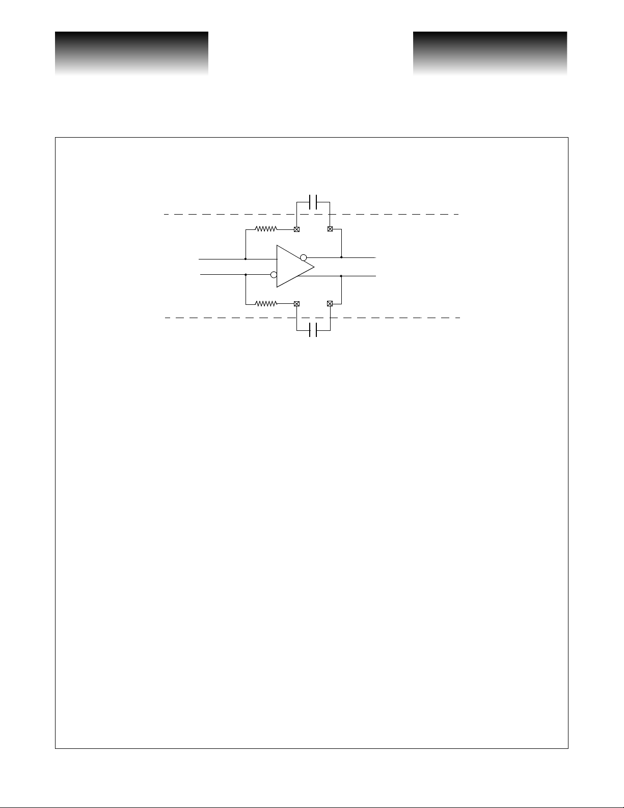
If the optics modules provide ECL level interface, the high speed sig nals can be AC coupled to the
VSC8113 as well. The PECL receiver inputs of the VSC8113 are internally biased at VDD/2. The refore, ACcoupling to the VSC8113 inputs is accomplished by providing the pull-down resistor for the open-source PECL
output and an AC-coupling capacitor used to eliminate the DC component of the output signal. This capacitor
allows the PECL receivers of the VSC8113 to self-bias via its internal resistor divider network (see Figure 13).
The PECL output drivers are capable of sourcing current but not sinking it. To establish a LOW output
level, a pull-down resistor, traditionally connected to VDD-2.0V, is needed when the output FET is turned off.
Since VDD-2.0V is usually not present in the system, the resistor could be terminated to ground for convenience. The VSC8113 output drivers should be either AC-coupled to the 5.0V PECL inputs of the optics module, or translated (DC le v el shift ). Appropr iate bia sing techniques f or setti ng the DC-l e v el of th ese input s should
be employed.
The dc biasing and 50 ohm termination requirements can easily be integrated together using a thevenin
equivalent circuit as shown in Figure 14. The figure shows the appropria te termin ation values wh en interfac ing
3.3V PECL to 5.0V PECL. This network provides the equivalent 50 ohm termination fo r the high speed I/Os
and also provides the requi red dc biasin g for the rec ei v ers of the opt ics modu le. Table 18 contains recommended
values for each of the components.
ATM/SONET/SDH 622 Mb/s Transceiver Mux/Demux
with Integrated Clock Generation and Clock Recovery
supply (VDDP) and are terminat ed to g ro und. To program
DDP
pins (pin 9, 15, 21) are required to connect to 3.3V or 5V
DDP
TTL Input Structure
The TTL inputs of the VSC8113 are 3.3V TTL which can accept 5.0V TTL levels within a given set of tolerances (see Table 5). The input structure, shown in Figure 14, uses a current limiter to avoid overdriving the
input FETs.
G52154-0, Rev 4.2
3/19/99 741 Calle Plano, Camarillo, CA 93012 • 805/388-3700 • FAX: 805/987-5896
VITESSE SEMICONDUCTOR CORPORATION
Page 25
Page 26

VITESSE
SEMICONDUCTOR CORPORATION
ATM/SONET/SDH 622 Mb/s Transceiver Mux/Demux
with Integrated Clock Generation and Clock Recovery
Layout of the High Speed Signals
Data Sheet
VSC8113
The routing of the High Speed signals should be done using good high speed design practices. This would
include using controlle d impedance lines and keep ing the distance between com ponents to an absolu te minimum. In addition, stubs should be kept at a minimum as well as any routing discontinuities. This will help minimize reflections and ringing on the high sp eed lines and insur e the maximum eye opening. I n addition the
output pull down resistor should be placed as close to the VSC8113 pin a s possible while the AC-coupling
capacitor and the biasing resistors should be placed as close as possible to the optics input pin. The same is true
on the receive circuit side. Using small outline components and minimum pad sizes also helps in reducing discontinuities.
Ground Planes
The ground plane for the components used in the High Speed interface should be continuous and not sectioned in an attempt to provide isolation to various components. Sectioning of the ground planes tends to interfere with the ground return currents on the signal lines. In addition, the smaller the ground plane s the less
effecti ve they are in redu cin g ground bounce noise and the more dif ficult to decouple. Sect ion in g of the positive
supplies can provide some isolation benefits.
Figure 13: AC Coupled High Speed I/O
+3.3V
DRIVER
(Optics Module)
PC Board Trace PC Board Trace
R1
GND
Table 19: AC Coupling Component Values
Component Value Tolerance
R1 270 ohms 5%
R2 75 ohms 5%
R3 68 ohms 1%
R4 190 ohms 1%
C1, C2, C3, C4 .01uf High Frequency
GND
Note: Only one side of a differential signal is shown.
VSC8113
PECL I/O
R2 R4
GND
C2C1
+5.0V
GND
RECEIVER
(Optics Module)
R3
Page 26
741 Calle Plano, Camarillo, CA 93012 • 805/388-3700 • FAX: 805/987-5896 3/19/99
VITESSE SEMICONDUCTOR CORPORATION
G52154-0, Rev 4.2
Page 27

VITESSE
SEMICONDUCTOR CORPORATION
Data Sheet
SC8113
INPUT
+3.3 V
V
DD
Current
Limit
R
R
GND
REFCLK and TTL Inputs
ATM/SONET/SDH 622 Mb/s Transceiver Mux/Demux
with Integrated Clock Generation and Clock Recovery
Figure 14: Input Structures
V
DDP
+3.3 /+5 V
INPUT
INPUT
GND
High Speed Differential Input
(RXDATAIN+/RXDATAIN-)
(RXCLKIN+/RXCLKIN-)
All Resistors
3.3K
+3.3 V
G52154-0, Rev 4.2
3/19/99 741 Calle Plano, Camarillo, CA 93012 • 805/388-3700 • FAX: 805/987-5896
VITESSE SEMICONDUCTOR CORPORATION
Page 27
Page 28

VITESSE
SEMICONDUCTOR CORPORATION
ATM/SONET/SDH 622 Mb/s Transceiver Mux/Demux
with Integrated Clock Generation and Clock Recovery
Data Sheet
VSC8113
Page 28
741 Calle Plano, Camarillo, CA 93012 • 805/388-3700 • FAX: 805/987-5896 3/19/99
VITESSE SEMICONDUCTOR CORPORATION
G52154-0, Rev 4.2
 Loading...