

Page 1

®
VITESSE Semiconductor Corporation
Page 1
VSC8110
Data Sheet
ATM/SONET/SDH 155/622 Mb/s Transceiv
er
Mux/Demux with Integrated Clock Generation
G51011-0, Rev. 1.5
VITESSE
Features
General Description
The VSC8110 is an ATM/SONET/SDH compatible transceiver integrating high speed clock generation
with 8 bit serial-to-parallel and parallel-to-serial data conversion. The high speed clock is generated using an
on-chip PLL which is selectable for 155.52 or 622.08 Mhz operation. The part can be used with 19.44, 38.88,
51.84 or 77.76 Mhz external reference clocks. The demultiplexer contains SONET/SDH frame detection and
recovery. In addition, the device provides both facility and equipment loopback modes. The part is packaged in
a 100PQFP with integrated heat spreader for optimum thermal performance and reduced cost. The VSC8110
provides an integrated solution for ATM physical layers and SONET/SDH systems applications.
Functional Description
The VSC8110 is designed to provide a SONET/SDH compliant interface between the high speed optical
networks and the lower speed User Network Interface devices such as the PM5355 S/UNI-622. The VSC8110
converts 8 bit parallel data at 77.76Mhz or 19.44Mhz to a serial bit stream at 622.08Mb/s or 155.52Mb/s respectively. The transmit section provides a Facility Loopback function which loops the received high speed data and
clock directly to the transmit outputs. A clock multiplier unit is integrated into the transmit circuit to generate
the high speed clock for the serial output data stream from input reference frequencies of 19.44, 38.88, 51.84 or
77.76 Mhz. The block diagram on page 2 shows the major functional blocks associated with the VSC8110.
The receive circuit provides the serial-to-parallel conversion, converting 155Mb/s or 622Mb/s to an 8 bit
parallel output at 19.44Mhz or 77.76Mhz respectively. The receive section provides an Equipment Loopback
function which will loop the high speed transmit data and clock back through the demultiplexer to the 8 bit parallel outputs.
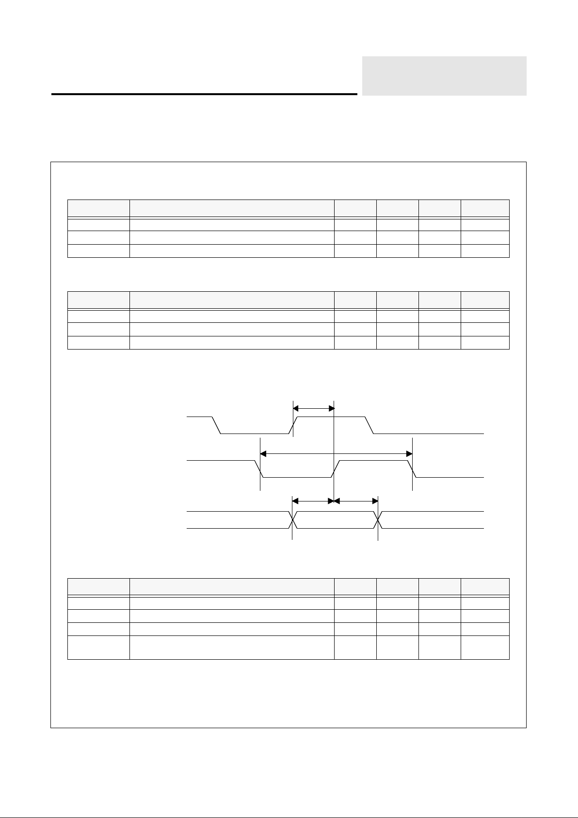
Transmit Circuit
Byte-wide data is presented to TXIN<7:0> and is clocked into the part on the rising edge of TXLSCKIN;
refer to Figure 1. The data is serialized (MSB leading) and presented at the TxOUT+/- pins. The Clock Multiplier Unit (CMU) generates the high speed clock required for serialization and transmission. The high speed
clock accompanying the transmitted data appears on the TxCLKOUT+/- pins. The reference clock is selectable
using the control lines BO-B2; refer to Table 13. The data rate (155Mb/s or 622Mb/s) is selected using the
STS12 control pin; refer to Table 13. The Facility Loopback mode is set by FACLOOP and is active high. A
51.84Mhz continuous clock (RX50MCK) is provided as a general board-level clock to drive other circuits such
as the UTOPIA interface on the UNI devices.
• Integrated PLL for Clock Generation - No
External Components
• SONET/SDH Frame Recovery
• Provides Equipment and F
acilities Loopback
• Low Power - 1.98 Watts Maximum
• Dual Supply Operation- +2, +5 Volts
• 100 PQFP Package
• Operates at Either STS-3/STM-1 (155.52 Mb/s)
or STS-12/STM-4 (622.08 Mb/s) Data Rates
• Compatible with Industry ATM UNI Devices
• On Chip Clock Generation of the 155.52 Mhz or
622.08 Mhz High Speed Clock
• Reference Clock Frequencies Selectable for
19.44, 38.88, 51.84 and 77.76 Mhz
• 8 bit Parallel TTL Interface
Page 2

VSC8110
VITESSE
Data Sheet
ATM/SONET/SDH 155/622 Mb/s Transceiver
Mux/Demux with Integrated Clock Generation
Page 2 ®
VITESSE
Semiconductor Corporation
G51011-0, Rev. 1.5
VSC8110 Block Diagram
EQULOOP
TxDATAOUT+
TxDATAOUT-
FACLOOP
RX50MCK
RXLSCKOUT
OOF
FP
RESET
TXIN<7:0>
TXLSCKIN
TXLSCKOUT
REFCLK+
REFCLK-
B0-B2
STS12
CMU
FRAME
DETECTION
RECOVERY
PARALLEL
TO SERIAL
3/12
FACILITY
LOOPBACK
REG
RxDATAIN+
RxDATAIN-
RXOUT<7:0>
SERIAL TO
PARALLEL
REG
0
1
0
1
EQUIPMENT
LOOPBACK
TxCLKOUT+
TxCLKOUT-
FACILITY
LOOPBACK
RxCLKIN+
RxCLKIN-
0
1
0
1
EQUIPMENT
LOOPBACK
8
8
Page 3

®
VITESSE Semiconductor Corporation
Page 3
VSC8110
Data Sheet
ATM/SONET/SDH 155/622 Mb/s Transceiv
er
Mux/Demux with Integrated Clock Generation
G51011-0, Rev. 1.5
VITESSE
Receive Circuit
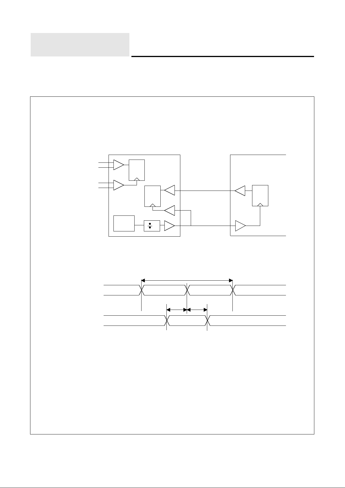
155Mb/s or 622Mb/s serial data and 155Mhz or 622Mhz clock are input to RxIN+/- and RxCLKIN+/- pins
respectively; refer to Figure 1. This data is converted to byte-wide parallel data and presented on RXOUT<7:0>
pins; refer to Figure 4. The received high speed clock is divided by 8 and presented on the RXLSCKOUT pin.
The receive circuit includes frame detection and recovery. The frame circuitry detects the SONET/SDH
frame, aligns the received serial data on byte boundaries, and initiates a frame pulse on FP coincident with the
byte aligned data. The frame recovery is initiated when OOF is held high which must occur at least 4 byte clock
cycles before the A1A2 boundary. OOF is a level-sensitive signal, and the VSC8110 will continually perform
frame detection and recovery as long as this pin is held high even if 1 or more frames has been detected. Frame
detection and recovery occurs when a series of three A1 bytes followed by three A2 bytes has been detected.
The parallel output data on RXOUT<7:0> will be byte aligned starting on the third A2 byte. When a frame is
detected, a pulse is generated on FP. The pulse FP is synchronized with the byte-aligned third A2 byte on
RXOUT<7:0>. The FP pulse is one byte clock period long. The frame detector sends an FP pulse only if OOF is
high or if a frame was detected while OOF was being pulled low.
Facility Loopback
The Facility Loopback function is controlled by the FACLOOP signal. When the FACLOOP signal is set
high, the Facility Loopback mode is activated and the high speed serial receive data (RxDATAIN) is presented
at the high speed transmit output (TxDATAOUT). In addition, the high speed receive clock input (RxCLKIN) is
selected and presented at the high speed transmit clock output (TxCLKOUT). In Facility Loopback mode the
high speed receive data (RxDATAIN) is also converted to parallel data and presented at the low speed receive
data output pins (RXOUT<7:0>). The receive clock (RxCLKIN) is also divided down and presented at the low
speed clock output (RXLSCKOUT). The Facility and Equipment Loopbacks are not designed to be enabled at
the same time.
Equipment Loopback
The Equipment Loopback function is controlled by the EQULOOP signal. When the EQULOOP signal is
set high, the Equipment Loopback mode is activated and the high speed transmit data generated from the parallel to serial conversion of the low speed data (TXIN<0:7>) is selected and converted back to parallel data on the
receiver circuit side and presented at the low speed parallel outputs (RXOUT<7:0>). The internally generated
155Mhz/622Mhz clock is used to generate the low speed receive clock output (RXLSCKOUT), (Note that the
clock presented at RXLSCKOUT can be changed to present the clock applied to the EXTCLKP/N pins if the
EXTVCO control pin is set active high. In this mode EXTCLK is also presented at the TXCLKOUT and
TXLSCKOUT pins.) In Equipment Loopback mode the transmit data (TXIN<7:0>) is serialized and presented
at the high speed output (TxDATAOUT) along with the high speed transmit clock (TxCLKOUT) which is generated by the on board clock multiplier unit. The facility and Equipment Loopbacks are not designed to be
enabled at the same time.
Page 4
VSC8110
VITESSE
Data Sheet
ATM/SONET/SDH 155/622 Mb/s Transceiver
Mux/Demux with Integrated Clock Generation
Page 4 ®
VITESSE
Semiconductor Corporation
G51011-0, Rev. 1.5
AC Timing Characteristics
Figure 1: Receive Data and Clock Block Diagram
Figure 2: Receive High Speed Data Input Timing Diagram
RxCLKIN -
RxDATAIN -
RxCLKIN +
RxDATAIN +
QD
CLK
Q
D
CLK
Q D
CLK
CMU
8
VSC8110
PM5355
TXLSCKOUT
TXIN<7:0>
TXLSCKIN
RxCLKIN -
RxDATAIN -
T
RXCLK
RxCLKIN +
RxDATAIN +
T
RXSUTRXH
Page 5
®
VITESSE Semiconductor Corporation
Page 5
VSC8110
Data Sheet
ATM/SONET/SDH 155/622 Mb/s Transceiv
er
Mux/Demux with Integrated Clock Generation
G51011-0, Rev. 1.5
VITESSE
Table 1: Receive High Speed Data Input Timing Table
(
STS-12 Operation )
Table 2: Receive High Speed Data Input Timing Table
(
STS-3 Operation )
Figure 3: Transmit Data Input Timing Diagram
Table 3: Transmit Data Input Timing Table
(
STS-12 Operation )
Note: Duty cycle for TXLSCKOUT is 50% +/- 5% worse case
Parameter Description Min Typ Max Units
T
RXCLK
Receive clock period - 1.608 - ns
T
RXSU
Serial data setup time with respect to RxCLKIN 500 - - ps
T
RXH
Serial data hold time with respect to RxCLKIN 500 - - ps
Parameter Description Min Typ Max Units
T
RXCLK
Receive clock period - 6.43 - ns
T
RXSU
Serial data setup time with respect to RxCLKIN 1.5 - - ns
T
RXH
Serial data hold time with respect to RxCLKIN 1.5 - - ns
Parameter Description Min Typ Max Units
T
CLKIN
Transmit data input byte clock period - 12.86 - ns
T
INSU
Transmit data setup time with respect to TXLSCKIN 1.0 - - ns
T
INH
Transmit data hold time with respect to TXLSCKIN 1.0 - - ns
T
PROP
Maximum allowable propagation delay for connecting
TXLSCKOUT to TXLSCKIN
- - 3 ns
T
INSU
T
INH
T
CLKIN
TXLSCKIN
TXIN<7:0>
TXLSCKOUT
(1)
T
PROP
Page 6
VSC8110
VITESSE
Data Sheet
ATM/SONET/SDH 155/622 Mb/s Transceiver
Mux/Demux with Integrated Clock Generation
Page 6 ®
VITESSE
Semiconductor Corporation
G51011-0, Rev. 1.5
Table 4: Transmit Data Input Timing Table
(
STS-3 Operation )
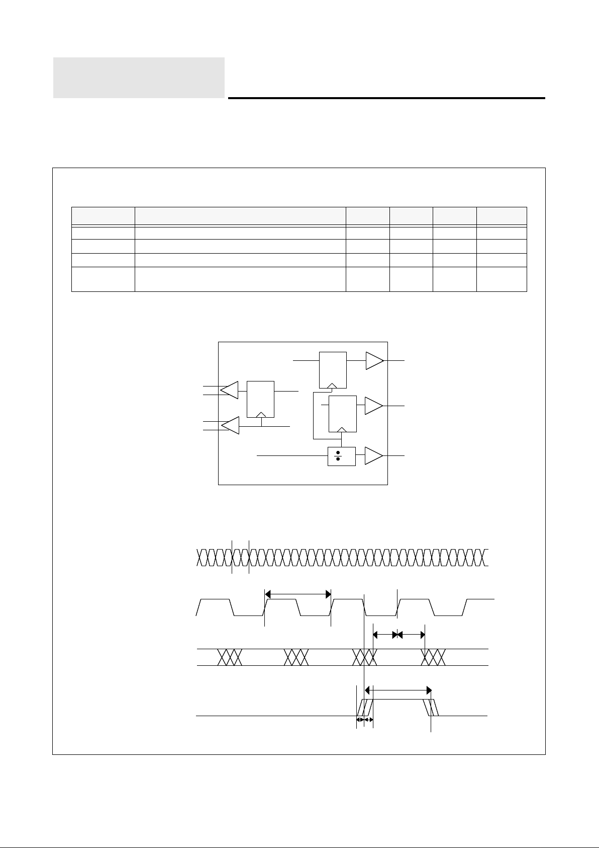
Figure 4: Data and Clock Transmit Block Diagram
Figure 5: Receive Data Output Timing Diagram
Parameter Description Min Typ Max Units
T
CLKIN
Transmit data input byte clock period - 51.44 - ns
T
INSU
Transmit data setup time with respect to TXLSCKIN 1.0 - - ns
T
INH
Transmit data hold time with respect to TXLSCKIN 1.0 - - ns
T
PROP
Maximum allowable propagation delay for connecting
TXLSCKOUT to TXLSCKIN
- - 3 ns
Q
D
CLK
VSC8110
FP
Q D
CLK
QD
CLK
TxDATA
TxCLK
RxDATA
RxCLK
TxCLKOUT -
TxDATAOUT -
TxCLKOUT +
TxDATAOUT +
RXLSCKOUT
RXOUT<7:0>
8
RxCLKIN -
FP
RxCLKIN +
T
PW
T
RXCLKIN
RXLSCKOUT
RXOUT<7:0> A1 A2A2A2
T
RXLSCK
T
SKEW
T
RXVALID
Page 7

®
VITESSE Semiconductor Corporation
Page 7
VSC8110
Data Sheet
ATM/SONET/SDH 155/622 Mb/s Transceiv
er
Mux/Demux with Integrated Clock Generation
G51011-0, Rev. 1.5
VITESSE
Table 5: Receive Data Output Timing Table
(
STS-12 Operation )
Table 6: Receive Data Output Timing Table
(
STS-3 Operation )
Figure 6: Transmit High Speed Data Timing Diagram
Parameter Description Min Typ Max Units
T
RXCLKIN
Receive clock period - 1.608 - ns
T
RXLSCK
Receive data output byte clock period - 12.86 - ns
T
SKEW
Range in which the rising edge of FP will appear in
relation to the falling edge of RXLSCKOUT
- - +/-1.5 ns
T
RXVALID
Time data on RXOUT<7:0> is valid before and after the
rising edge of RXLSCKOUT
4.9 - - ns
T
PW
Pulse width of frame detection pulse FP - 12.86 - ns
Parameter Description Min Typ Max Units
T
RXCLKIN
Receive clock period - 6.43 - ns
T
RXLSCKT
Receive data output byte clock period - 51.44 - ns
T
SKEW
Range in which the rising edge of FP will appear in
relation to the falling edge of RXLSCKOUT
- - +/-1.5 ns
T
RXVALID
Time data on RXOUT<7:0> is valid before and after the
rising edge of RXLSCKOUT
24 - - ns
T
PW
Pulse width of frame detection pulse FP - 51.44 - ns
TxCLKOUT+
TxDATAOUT+
T
SKEW
TxCLKOUT-
TxDATAOUT-
T
TXCLK
Page 8

VSC8110
VITESSE
Data Sheet
ATM/SONET/SDH 155/622 Mb/s Transceiver
Mux/Demux with Integrated Clock Generation
Page 8 ®
VITESSE Semiconductor Corporation
G51011-0, Rev. 1.5
Table 7: Transmit High Speed Data Timing Table
(
STS-12 Operation
)
Table 8: Transmit High Speed Data Timing Table
(
STS-3 Operation
)
Data Latency
The VSC8110 contains several operating modes, each of which exercise different logic paths through the
part. Table 9 bounds the data latency through each path with an associated clock signal.
Table 9: Data Latency
Parameter Description Min Typ Max Units
T
TXCLK
Transmit clock period - 1.608 - ns
T
SKEW
Skew between the falling edge of TxCLKOUT and valid
data on TxDATAOUT
- - +/-200 ps
Parameter Description Min Typ Max Units
T
TXCLK
Transmit clock period - 6.43 - ns
T
SKEW
Skew between the falling edge of TxCLKOUT and valid
data on TxDATAOUT
- - +/-200 ps
Circuit
Mode
Description
Clock
Reference
Range of
Clock cycles
STS-12
Range of
Clock cycles
STS-3
Transmit Data TXIN<7:0> to MSB at TxDATAOUT TxCLKOUT 2-11 2-11
Receive MSB at RxDATAIN to data on RXOUT<7:0> RxCLKIN 18-25 15-22
Equipment
Loopback
Byte data TXIN<7:0> to byte data on RXOUT<7:0> TxCLKOUT 19-33 17-31
Facilities
Loopback
MSB at RxDATAIN to MSB at TxDATAOUT RxCLKIN 10 10
Page 9

®
VITESSE Semiconductor Corporation
Page 9
VSC8110
Data Sheet
ATM/SONET/SDH 155/622 Mb/s Transceiv
er
Mux/Demux with Integrated Clock Generation
G51011-0, Rev. 1.5
VITESSE
Absolute Maximum Ratings
(1)
Power Supply Voltage (
VMM) Potential to GND............................................................................-0.5V to +2.5V
Power Supply Voltage (
V
TTL
) Potential to GND............................................................................-0.5V to +5.5V
TTL Input Voltage Applied ................................................................................................. -0.5V to V
TTL
+ 1.0V
VECL Input Voltage Applied .............................................................................................. -0.5V to V
MM
+ 1.0V
Output Current (
I
OUT
).................................................................................................................................. 50mA
Case Temperature Under Bias (
TC)................................................................................................-55o to + 125oC
Storage Temperature (
T
STG
)..........................................................................................................-65o to + 150oC
Note: Caution: Stresses listed under “Absolute Maximum Ratings” may be applied to devices one at a time without causing
permanent damage. Functionality at or exceeding the values listed is not implied. Exposure to these values for extended
periods may affect device reliability.
Recommended Operating Conditions
Power Supply Voltage (
VMM)...............................................................................................................+2.0V %
Power Supply Voltage (
V
TTL
)...............................................................................................................+5.0V %
Commercial Operating Temperature Range* (
T
).................................................................................. 0o to 70oC
* Lower limit of specification is ambient temperature and upper limit is case temperature.
ESD Ratings
Proper ESD procedures should be used when handling this product. The VSC8110 is rated to the following
ESD voltages based on the human body model:
1. All pins are rated at or above 1500V.
5 ±
5 ±
Page 10

VSC8110
VITESSE
Data Sheet
ATM/SONET/SDH 155/622 Mb/s Transceiver
Mux/Demux with Integrated Clock Generation
Page 10 ®
VITESSE Semiconductor Corporation
G51011-0, Rev. 1.5
DC Characteristics
Table 10: VECL Inputs and Outputs
Note: Differential VECL output pins must be terminated identically.
Table 11: TTL Inputs and Outputs
Parameter Description Min Typ Max Units Conditions
V
OH
Output HIGH voltage VMM-1020 - VMM-850 mV 50 ohm to gnd
V
OL
Output LOW voltage VMM-2000 - VMM-1620 mV 50 ohm to gnd
V
IH
Input HIGH voltage VMM-1100 - VMM-700 mV
Guaranteed HIGH
signal for all inputs
V
IL
Input LOW voltage VMM-
2000
- VMM-1540 mV
Guaranteed LOW
signal for all inputs
I
IH
Input HIGH current - - 200 uA VIN=VIH (max)
I
IL
Input LOW current -50 - - uA VIN=VIL (min)
V
DIFF
Input Voltage Differential 200 - - mV
V
CM
Common Mode Voltage VMM-1.5 - VMM-0.5 V
Parameter Description Min Typ Max Units Conditions
V
OH
Output HIGH voltage 2.4 - - mV
V
IN
= VIH (max)
or V
IL
(min)
IOH=-2.4mA
V
OL
Output LOW voltage 0 - 0.5 mV
V
IN
= VIH (max)
or V
IL
(min)
IOL=8mA
V
IH
Input HIGH voltage 2.0 -
V
TTL
+1.
0
mV
Guaranteed HIGH
signal for all inputs
V
IL
Input LOW voltage 0 - 0.8 mV
Guaranteed LOW
signal for all inputs
I
IH
Input HIGH current - - 50 uA VIN=VIH (max)
I
IL
Input LOW current -500 - - uA VIN=VIL (min)
I
OZH
3-State Output OFF current HIGH - - 200 uA V
OUT
=2.4V
I
OZL
3-State Output OFF current LOW -200 - - uA V
OUT
=0.5V
Page 11

®
VITESSE Semiconductor Corporation
Page 11
VSC8110
Data Sheet
ATM/SONET/SDH 155/622 Mb/s Transceiv
er
Mux/Demux with Integrated Clock Generation
G51011-0, Rev. 1.5
VITESSE
Power Dissipation
Table 12: Power Supply Currents
Note: Specified with outputs open circuit. The combined maximum currents (IMM, I
TTL
) for any part will not exceed 1.98 Watts.
Clock Multiplier Unit
Table 13: Reference Frequency Selection and Output Frequency Control
Table 14: Clock Multiplier Unit Performance
Note: Jitter specification is defined utilizing a 12KHz - 5MHz LP-HP single pole filter.
Parameter Description (Max) Units
I
MM
Power supply current from V
MM
430 mA
I
TTL
Power supply current from V
TTL
218 mA
P
D
Power dissipation 1.98 W
STS12 B2 B1 B0
Reference
Frequency
[MHz]
Output
Frequency
[MHz]
1 1 1 0 19.44 622.08
1 0 1 0 38.88 622.08
1 0 0 1 51.84 622.08
1 0 0 0 77.76 622.08
0 1 1 0 19.44 155.52
0 0 1 0 38.88 155.52
0 0 0 1 51.84 155.52
0 0 0 0 77.76 155.52
Name Description Min Typ Max Units
RCd Reference clock duty cycle 40 60 %
RCj Reference clock jitter (RMS) 5 ps
OCd Output clock duty cycle 40 60 %
OCj Output clock jitter (RMS) @ 77.76 MHz ref 8 ps
OCj Output clock jitter (RMS) @ 51.84 MHz ref 10 ps
OCj Output clock jitter (RMS) @ 38.88 MHz ref 13 ps
OCj Output clock jitter (RMS) @ 19.44 MHz ref 15 ps
OCfmin Minimum output frequency 620 MHz
OCfmax Maximum output frequency 624 MHz
Page 12

VSC8110
VITESSE
Data Sheet
ATM/SONET/SDH 155/622 Mb/s Transceiver
Mux/Demux with Integrated Clock Generation
Page 12 ®
VITESSE Semiconductor Corporation
G51011-0, Rev. 1.5
Package Pin Description
Table 15: Pin Definitions
Signal Pin I/O Level Pin Description
FACLOOP 1 I TTL Facility loopback, active high
VMM 2 +2V +2 volt supply
_VSCTE 3 I TTL Test pin enable. Tie low for system operation
RESET 4 I TTL
Resets frame detection, dividers, controls, and tristates TTL
outputs; active high
EXTVCO 5 I TTL Test mode control; tie low for system operation
B0 6 I TTL Reference clock select, refer to table 13
B1 7 I TTL Reference clock select, refer to table 13
B2 8 I TTL Reference clock select, refer to table 13
VMM 9 +2V +2 volt supply
TxDATAOUT+ 10 O VECL Transmit output, high speed differential data +
TxDATAOUT- 11 O VECL Transmit output, high speed differential data VCC 12 GND Ground
TxCLKOUT+ 13 O VECL Transmit high speed clock differential output+
TxCLKOUT- 14 O VECL Transmit high speed clock differential outputVMM 15 +2V +2 volt supply
EXTCLKP 16 I VECL
External clock input+, test mode only; tie to V
MM
for system
operation
EXTCLKN 17 I VECL
External clock input-, test mode only; tie to ground for system
operation
VCC 18 GND Ground
RxCLKIN+ 19 I VECL Receive high speed differential clock input+
RxCLKIN- 20 I VECL Receive high speed differential clock inputVMM 21 +2V +2 volt supply
OOF 22 I TTL Out Of Frame; Frame detection initiated with high level
NC 23 No connection
RxDATAIN+ 24 I VECL Receive high speed differential data input+
RxDATAIN- 25 I VECL Receive high speed differential data inputNC 26 No connection
NC 27 No connection
VMM 28 +2V +2 volt supply
NC 29 No connection
Page 13

®
VITESSE Semiconductor Corporation
Page 13
VSC8110
Data Sheet
ATM/SONET/SDH 155/622 Mb/s Transceiv
er
Mux/Demux with Integrated Clock Generation
G51011-0, Rev. 1.5
VITESSE
_VSCIPNC 30 I TTL Test mode input. Tie low for system operation
VTTL 31 +5.0V +5 volt supply
_VSCOPNC 32 O VECL Test mode output
RX50MCK 33 O TTL
Constant 51.84Mhz reference clock output, derived from the
Clock Multiplier Unit
VCC 34 GND Ground
RXOUT0 35 O TTL Receive output data bit0
RXOUT1 36 O TTL Receive output data bit1
VCC 37 GND Ground
RXOUT2 38 O TTL Receive output data bit2
RXOUT3 39 O TTL Receive output data bit3
VCC 40 GND Ground
RXOUT4 41 O TTL Receive output data bit4
RXOUT5 42 O TTL Receive output data bit5
VCC 43 GND Ground
RXOUT6 44 O TTL Receive output data bit6
RXOUT7 45 O TTL Receive output data bit7
VCC 46 GND Ground
RXLSCKOUT 47 O TTL Receive byte clock output
FP 48 O TTL Frame detection pulse
VTTL 49 +5.0V +5 volt supply
NC 50 No connection
NC 51 No connection
NC 52 No connection
NC 53 No connection
VMM 54 +2V +2 volt supply
VCC 55 GND Ground
REFCLK+ 56 I VECL Differential reference clock input+, refer to table 13
REFCLK- 57 I VECL Differential reference clock input-, refer to table 13
VTTL 58 +5.0V +5 volt supply (CMU)
VCC 59 GND Ground (CMU)
VCC 60 GND Ground (CMU)
NC 61 No connection
NC 62 No connection
Signal Pin I/O Level Pin Description
Page 14

VSC8110
VITESSE
Data Sheet
ATM/SONET/SDH 155/622 Mb/s Transceiver
Mux/Demux with Integrated Clock Generation
Page 14 ®
VITESSE Semiconductor Corporation
G51011-0, Rev. 1.5
NC 63 No connection
NC 64 No connection
NC 65 No connection
NC 66 No connection
VTTL 67 +5.0V +5 volt supply (CMU)
VTTL 68 +5.0V +5 volt supply (CMU)
VTTL 69 +5.0V +5 volt supply (CMU)
VCC 70 GND Ground (CMU)
VCC 71 GND Ground (CMU)
VCC 72 GND Ground (CMU)
NC 73 No connection
NC 74 No connection
VCC 75 GND Ground
VMM 76 +2V +2 volt supply
NC 77 No connection
NC 78 No connection
NC 79 No connection
NC 80 No connection
VTTL 81 +5.0V +5 volt supply
TXLSCKOUT 82 O TTL Transmit byte clock out
TXLSCKIN 83 I TTL Transmit byte clock in
VCC 84 GND Ground
TXIN7 85 I TTL Transmit input data bit7
TXIN6 86 I TTL Transmit input data bit6
VCC 87 GND Ground
TXIN5 88 I TTL Transmit input data bit5
TXIN4 89 I TTL Transmit input data bit4
NC 90 No connection
TXIN3 91 I TTL Transmit input data bit3
TXIN2 92 I TTL Transmit input data bit2
VCC 93 GND Ground
TXIN1 94 I TTL Transmit input data bit1
TXIN0 95 I TTL Transmit input data bit0
NC 96 No connection
Signal Pin I/O Level Pin Description
Page 15

®
VITESSE Semiconductor Corporation
Page 15
VSC8110
Data Sheet
ATM/SONET/SDH 155/622 Mb/s Transceiv
er
Mux/Demux with Integrated Clock Generation
G51011-0, Rev. 1.5
VITESSE
The VSC8110 is manufactured in a 100PQFP package which is supplied by two different vendors. The critical dimensions in the drawing represent the superset of dimensions for both packages. The significant difference between the two packages is in the shape and size of the heatspreader which needs to be considered when
attaching a heatsink.
Package Thermal Characteristics
The VSC8110 is packaged in a thermally enhanced 100PQFP with an embedded heat sink. The heat sink
surface configurations are shown in the package drawings. With natural convection, the case to air thermal resistance is estimated to be 27.5
o
C/W. The air flow versus thermal resistance relationship is shown in table 16.
Table 16: Theta Case to Ambient versus Air Velocity
STS12 97 I TTL 155Mb/s or 622Mb/s mode select, refer to table 13
PLLM 98 O VECL PLL test output, leave unconnected in system operation
VTTL 99 +5.0V +5 volt supply
EQULOOP 100 I TTL Equipment loopback, active high
Air Velocity
(LFPM)
Case to air thermal resistance
o
C/W
0 27.5
100 23.1
200 19.8
400 17.6
600 16
Signal Pin I/O Level Pin Description
Page 16

VSC8110
VITESSE
Data Sheet
ATM/SONET/SDH 155/622 Mb/s Transceiver
Mux/Demux with Integrated Clock Generation
Page 16 ®
VITESSE Semiconductor Corporation
G51011-0, Rev. 1.5
Package Information
NOTES:
(1) Drawings not to scale.
(2) Two styles of exposed heat spreaders
(3) All units in millimeters
may be used; square or oval.
Dims. mm
Tolerance
A 3.40 MAX
A1 0.60 MAX
A2 2.7 ±.10
D 17.20 ±.40
D1 14.00 ±.10
E 23.20 ±.40
E1 20.00 ±.10
L 0.80 ±.2
e 0.65 NOM
b 0.30 ±.10
θ 0-10°
R .25 ΝΟΜ
R1 .2 NOM
RAD 2.92 ± .50
(2X)
2.54±.50
(2X)
PIN 100
PIN 1
HEATSINK
INTRUSION
9.0 X 9.0
D1
D
E1
E
e
A
2
100 PQFP Package Drawings
R
R
1
A
A
1
b
L
0.25
0.20 MAX
θ
0° - 10°
Page 17

®
VITESSE Semiconductor Corporation
Page 17
VSC8110
Data Sheet
ATM/SONET/SDH 155/622 Mb/s Transceiv
er
Mux/Demux with Integrated Clock Generation
G51011-0, Rev. 1.5
VITESSE
Ordering Information
The order numbers for this product are:
Part Number Device Type
VSC8110QB: 155Mb/s-622Mb/s Mux/Dmux with CMU in 100 Pin PQFP
Commercial temperature, 0
°
C ambient to 70° case
VSC8110QB1: 155Mb/s-622Mb/s Mux/Dmux with CMU in 100 Pin PQFP
Extended temperature, 0
°
C ambient to 110° case
VSC8110QB2: 155Mb/s-622Mb/s Mux/Dmux with CMU in 100 Pin PQFP
Industrial temperature, -40
°
C ambient to 85°C case
Notice
Vitesse Semiconductor Corporation reserves the right to make changes in its products, specifications or other
information at any time without prior notice. Therefore the reader is cautioned to confirm that this datasheet is current
prior to placing any orders. The company assumes no responsibility for any circuitry described other than circuitry
entirely embodied in a Vitesse product.
Warning
Vitesse Semiconductor Corporation’s product are not intended for use in life support appliances, devices or sys-
tems. Use of a Vitesse product in such applications without the written consent is prohibited.
Page 18

VSC8110
VITESSE
Data Sheet
ATM/SONET/SDH 155/622 Mb/s Transceiver
Mux/Demux with Integrated Clock Generation
Page 18 ®
VITESSE Semiconductor Corporation
G51011-0, Rev. 1.5
Application Notes
2 Volt Supply Generation From 5 Volts
The 2 volt supply can be generated from the 5 volt supply using a linear regulator. There are many manufac-
turers who supply linear regulators. Refer to Table 17 for examples.
Table 17: Recommended 2 Volt Voltage Regulator
Interconnecting the Byte Clocks (TXLSCKOUT and TXLSCKIN)
The byte clock (TXLSCKOUT and TXLSCKIN) on the VSC8110 has been brought off-chip to allow as
much flexibility in system-level clocking schemes as possible. Since the byte clock (TXLSCKOUT) clocks both
the VSC8110 and the UNI devices, it is important to pay close attention to the routing of this signal. The UNI
device in general is a CMOS part which can have very wide spreads in timing (1-11ns clock in to parallel data
out for the PM5355), which utilizes most of the 12.86ns period (at 78Mhz), leaving little for the trace delays
and set-up times required to interconnect the 2 devices. The recommended way of routing this clock when used
in a 622Mhz mode is to daisy chain it to the UNI device pin and then route it back to the VSC8110 along with
the byte data. This eliminates the 1-way trace delay that would otherwise be encountered between the data and
clock and thus leaves 1.86ns for the VSC8110 setup time and for variations in trace delays and rise times
between clock and data. The trace delay must be kept under 2ns (allowing an additional 1ns for v ariations in rise
times and skews) to ensure proper muxing of parallel input data into the VSC8110; reference Table 3 and 4.
AC Coupling and Terminating High-speed I/Os
The high speed signals on the VSC8110 (RxDATAIN, RxCLKIN, TxDATAOUT, TxCLKOUT) use VECL
levels which are essentially ECL levels shifted positive by 2 volts. The VECL I/Os are referenced to the V
MM
supply and are terminated to ground. Since most optics modules use either ECL or PECL levels, the high speed
ports need to be ac coupled to overcome the difference in dc levels. In addition, the inputs must be dc biased to
hold the inputs at their threshold value with no signal applied. The dc biasing and 50 ohm termination requirements can easily be integrated together using a thevenin equivalent circuit as shown in Figure 8. The figure
shows the appropriate termination values when interfacing PECL to VECL and VECL to PECL. This network
provides the equivalent 50 ohm termination for the high speed I/Os and also provides the required dc biasing for
both the drivers and receivers. Table 18 contains recommended values for each of the components.
Layout of the 622 Signals
The routing of the 622 signals should be done using good high speed design practices. This would include
using controlled impedance lines and keeping the distance between components to an absolute minimum. In
addition, stubs should be kept at a minimum as well as any routing discontinuities. This will help minimize
reflections and ringing on the high speed lines and insure the maximum eye opening. In addition the output pull
Recommended Regulator Maximum Supply Current Manufacturer’s Information
REG1117 800mA
Burr Brown
800-548-6132
LT117A 800mA Linear Technology
Page 19

®
VITESSE Semiconductor Corporation
Page 19
VSC8110
Data Sheet
ATM/SONET/SDH 155/622 Mb/s Transceiv
er
Mux/Demux with Integrated Clock Generation
G51011-0, Rev. 1.5
VITESSE
down resistor should be placed as close to the VSC8110 pin as possible while the AC-coupling capacitor and
the biasing resistors should be placed as close as possible to the optics input pin. The same is true on the receive
circuit side. Using small outline components and minimum pad sizes also helps in reducing discontinuities.
Ground Planes
The ground plane for the components used in the 622 interface should be continuous and not sectioned in
an attempt to provide isolation to various components. Sectioning of the ground planes tends to interfere with
the ground return currents on the signal lines as well as in general, the smaller the ground planes the less effective they are in reducing ground bounce noise and the more difficult to decouple etc. Sectioning of the positive
supplies can provide some isolation benefits.
Reference Clock Generation
It has been noted that additional jitter may be generated on the reference clock if a TTL Oscillator is level
shifted using a TTL to ECL converter. The best recommendation is to use an ECL oscillator which can be ACcoupled straight into the REF CLOCK inputs on the VSC8110
.
Figure 7: AC Coupled High Speed I/O
Table 18: AC Coupling Component Values
Component Value Tolerance
R1 270 ohms 1%
R2 147 ohms 1%
R3 76 ohms 1%
R4 50 - 100 ohms 1%
R5 68 ohms 1%
R6 190 ohms 1%
C1, C2, C3, C4 .01uf High Frequency
VCC Ground
Receiver
V
CC
Ground
Driver
R1
VCC Ground
C1
Receiver
VMM +2 Volt Supply
Driver
R4
C3
R2
R3
C2
PECL
Output
R5
R6
C4
PECL
Input
VSC8110
VECL
Input/Output
+ 5 Volt Supply + 5 Volt Supply
Page 20

VSC8110
VITESSE
Data Sheet
ATM/SONET/SDH 155/622 Mb/s Transceiver
Mux/Demux with Integrated Clock Generation
Page 20 ®
VITESSE Semiconductor Corporation
G51011-0, Rev. 1.5
 Loading...