

Page 1
®
VITESSE Semiconductor Corporation
Page 1
VSC8101/8102
Preliminary Data Sheet
155.52 Mb/s Cloc
k and
Data Recovery Units
G52087-0 Rev. 1.3
VITESSE
Features
Functional Description
The VSC8101 and VSC8102 are clock and data recovery units for STS-3 (155.52 Mb/s) applications. They
implement the complete clock and data recovery functions and require no external components. The one-channel device, VSC8101, accepts serial data in NRZ or NRZI format and re-times the data using a sampling clock
extracted from the input data stream. The recovered clock (RCLK+/-) and re-timed data (RDAT+/-) are presented at the serial output ports, aligned such that the falling edge of the recovered clock (RCLK+) coincides
with the center of the data eye (see figure 4). The VSC8102 is an octal version of the VSC8101. A single reference clock input (REFCK+/-) at the STS-3 data rate (155.52MHz) is required for either device. The data and
reference clock inputs, and the recovered data and clock outputs are differential ECL levels referenced to the
V
CC
supply. Only one supply, +2V or -2V, is required for operation.
Both the VSC8101 and VSC8102 employ a digital clock extraction technique, and do not contain a con ventional PLL. As a result, the spectrum of the jitter in the recovered clock and data is non-Gaussian. Peak-to-peak
jitter of RCLK+/- is
±
400 ps or less. The data input rate to the devices is required to be within ± 30 ppm from
the reference clock frequency. The devices have data input jitter accommodation up to 3.2ns, half the data
period. The VSC8101and VSC8102 also provide an input which control the loop bandwidth of the clock extraction function.
Tracking Frequency Bandwidth Control
The tracking of the recovered clock and data to the frequency variation of the input data stream can be
adjusted in the VSC8101 and VSC8102. In particular, the FILTER0 input controls the degree to which the internal clock can track the input data frequency. The effect is equivalent to controlling the loop bandwidth of a conventional PLL-based clock recovery system. Equivalent bandwidths of 150 KHz and 10 KHz can be selected.
The FILTER0 input truth data is shown in the AC Characteristic Table.
Jitter Tolerance
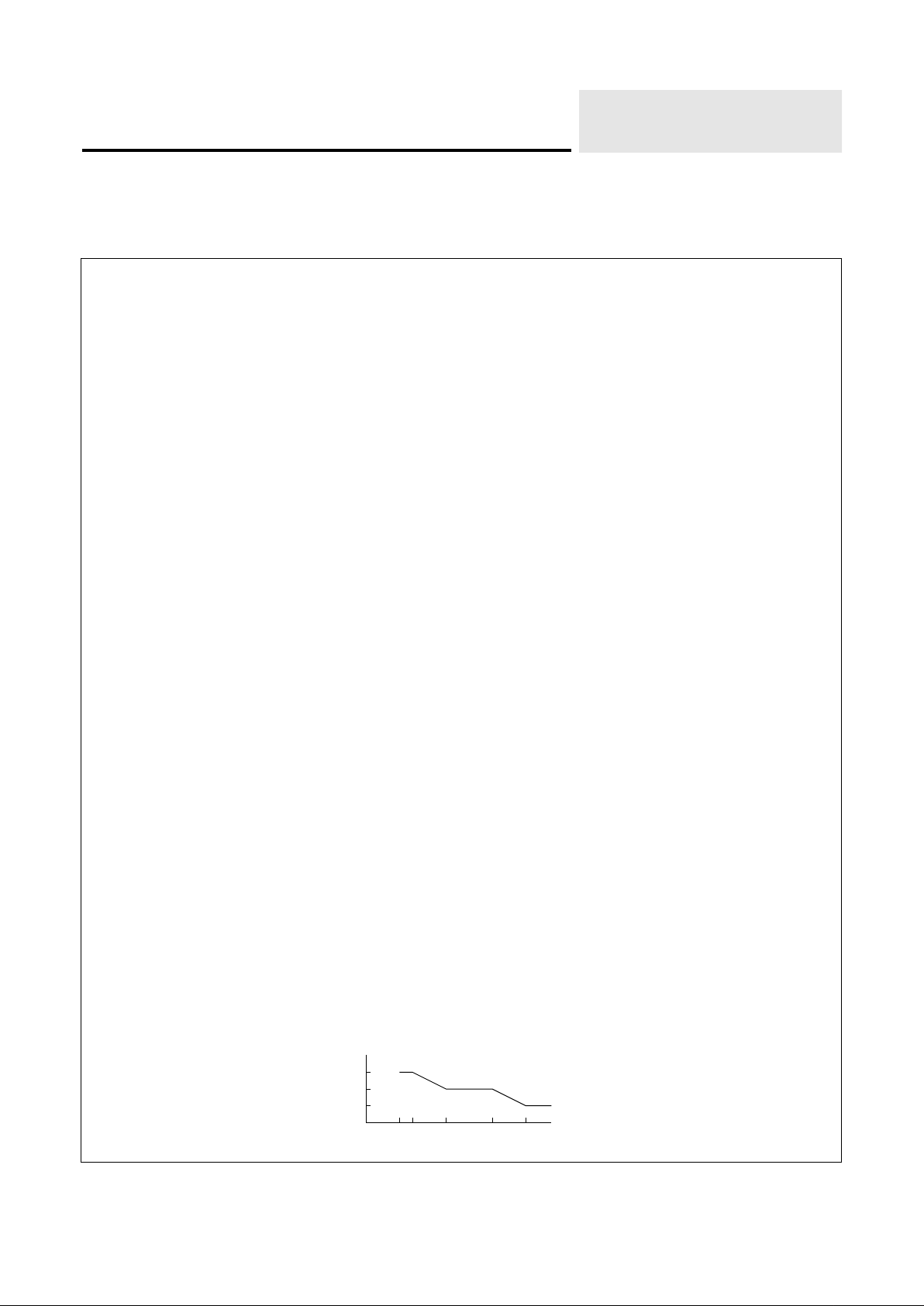
The VSC8101 and VSC8102 are designed to meet the BellcoreGR-253-CORE, section 5.6.2.2.2 Jitter Tolerance specification.
Figure 1: Jitter Tolerance Mask for STS-3
Jitter Amplitude
(UI p-p)
Frequency (Hz)
10 30 300 6.5K 65K
15
1.5
0.15
• Recovers Clock and Data at STS-3 (155.52 Mb/s)
Data Rate.
• No External Components Required.
• Available in One-channel (VSC8101) or
Eight-channel (VSC8102) Versions.
• Recovers Data from NRZ or NRZI Data Streams.
• No Output Clock Drift in Absence of Data
Transitions Once Lock is Acquired.
• ECL or Psuedo ECL (PECL) Differential Inputs
and Outputs.
• Maximum Power Dissipation:
VSC8101: 400mW,
VSC8102: 3W.
• Single 2V Power Supply
• Available in 28PLCC (VSC8101)
and 100PQFP (VSC8102)
Page 2

VSC8101/8102
VITESSE
Preliminar
y Data Sheet
155.52 Mb/s Clock and
Data Recovery Units
Page 2 ®
VITESSE
Semiconductor Corporation
G52087-0 Rev. 1.3
Figure 2: VSC8101 Block Diagram
Figure 3: VSC8102 Block Diagram
Delay
Digital
Clock
Recovery
SDAT +
SDAT -
RDAT+
RDAT -
RCLK +
RCLK -
Data
Retimer
REFCK +
FILTER0
REFCK -
Delay
Digital
Clock
Recovery
SDAT1 +
SDAT1 -
REFCK +
RDAT1 +
RDAT1 -
RCLK1 +
RCLK1-
FILTER0
Data
Retimer
Delay
Digital
Clock
Recovery
SDAT2 +
SDAT2 -
RDAT2 +
RDAT2 -
RCLK2 +
RCLK2 -
Data
Retimer
Delay
Digital
Clock
Recovery
SDAT8 +
SDAT8 -
RDAT8 +
RDAT8 -
RCLK8 +
RCLK8 -
Data
Retimer
REFCK -
Page 3
®
VITESSE Semiconductor Corporation
Page 3
VSC8101/8102
Preliminary Data Sheet
155.52 Mb/s Cloc
k and
Data Recovery Units
G52087-0 Rev. 1.3
VITESSE
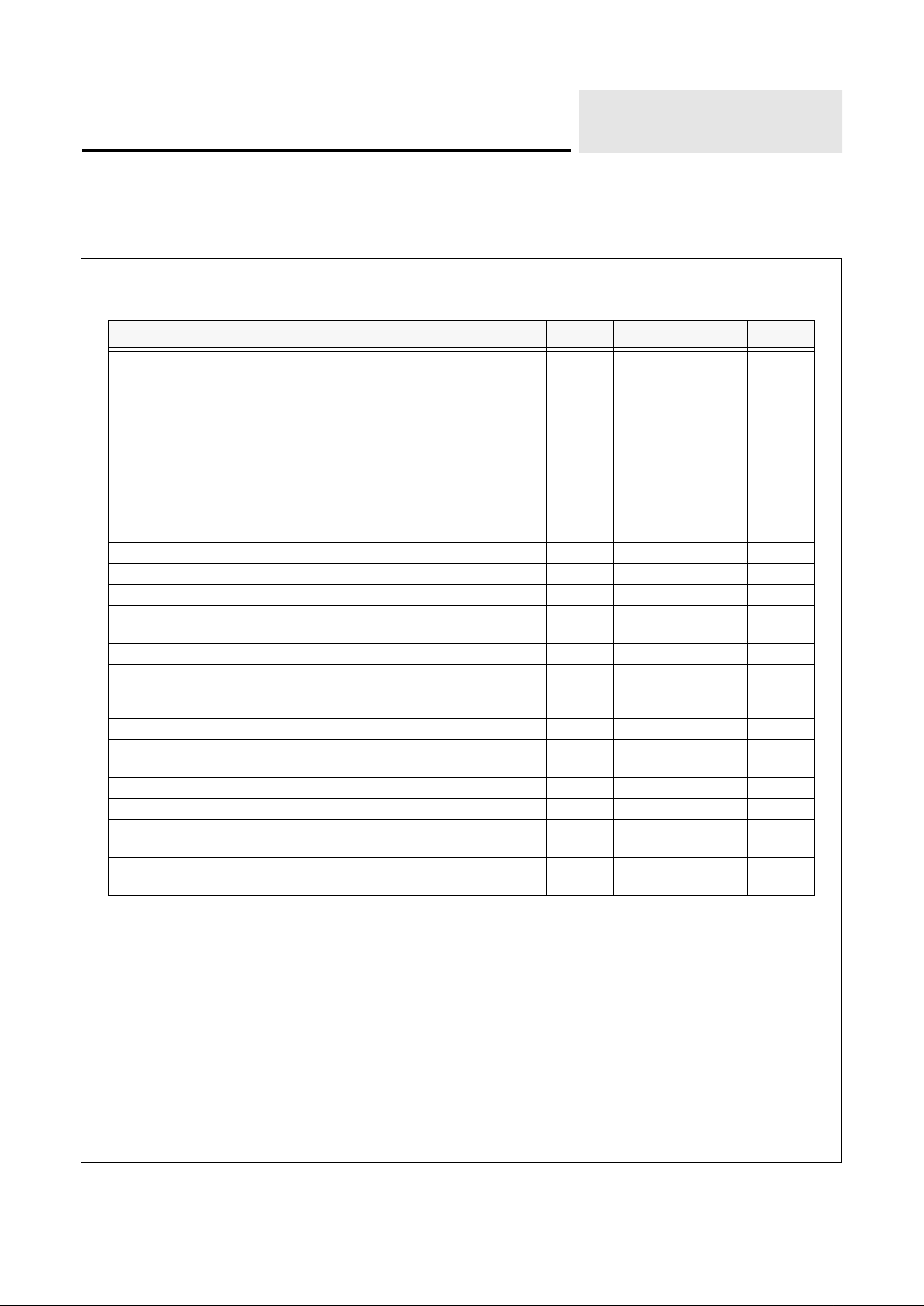
VSC8101/8102 AC Characteristics
(Over recommended operating range
Notes: (1) The part is designed to operate at 155.52 MHz. A reference clock with frequency variation of +/- 50 ppm or better is rec-
ommended. Consult the factory for applications other than this frequency.
(2) With minimum 50% Input Data Eye opening at 155.52 Mb/s.
. (3) With a jitter-free data input and minimum transition density of 50%.
Parameter Description Min Typ Max Units
t
CLK
REFCK+/- Input Clock period
(1)
— 6.43 — ns
t
DCYC
SDAT +/- Input data period
t
CLK
-
30 ppm
—
t
CLK
+
30 ppm
f
DC
SDAT+/- Input Rate Difference with respect to
REFCK+/-
-30 — +30 ppm
t
CDC
REFCK+/- Duty Cycle 40 — 60 %
t
DH
Recovered Data hold time from falling edge of
Recovered Clock
(2)
2.5 — 3.9 ns
t
DS
Recovered Data setup time to falling edge of
Recovered Clock
(2)
2.5 — 3.9 ns
t
RCH
RCLK+/- Recovered Clock Output High Pulse Width 2.6 — — ns
t
RCL
RCLK+/- Recovered Clock Output Low Pulse Width 2.6 — — ns
t
RCYC
RCLK+/- Recovered Clock Period 6.0 — 6.8 ns
t
DJA
SDAT+/- Input Jitter Accommodation (DC to 20 MHz)
Peak-to-peak
— — 3.2 ns
t
LA
Lock Acquisition Time
(3)
— — 5.0 s
f
BW
Loop Bandwidth:
a) at FILTER0 = Lo
b) at FILTER0 = Hi
— — 150
10
KHz
t
RCJ
RCLK+/- Recovered Clock Jitter -400 400 ps
t
PD
Propagation Delay from SDATA+/- Input to RDAT+/Output
— — TBD ps
t
Cr
,
t
Cf
REFCK+/- Input rise and fall time, 20% to 80% — — 1.2 ns
t
SDr
,
t
SDf
SDATA+/- Input rise and fall time, 20% to 80% — — 1.2 ns
t
RCr
,
t
RCf
RCLK+/- Recovered Clock Output rise and fall time,
20% to 80%
300 — 800 ps
t
RDr
,
t
RDf
RDAT+/- Recovered Data Output rise and fall time,
20% to 80%
300 — 800 ps
∆
µ
Page 4

VSC8101/8102
VITESSE
Preliminar
y Data Sheet
155.52 Mb/s Clock and
Data Recovery Units
Page 4 ®
VITESSE
Semiconductor Corporation
G52087-0 Rev. 1.3
Figure 4: VSC8101/8102 AC Timing Waveform
Absolute Maximum Ratings
(1)
Power Supply Voltage ( V
CC
-
V
TT
)..................................................................................................-0.5V to +3.0V
Input Voltage (
V
IN
) ...................................................................................................... V
CC
-2.5V to V
CC
+ 0.5V
Output Current,
I
OUT
(DC, Output HI) .......................................................................................................-50mA
Case Temperature Under Bias,
T
C
................................................................................................. -55 ° to +125 ° C
Storage Temperature (
T
STG
)........................................................................................................-65 ° C to +135 ° C
Recommended Operating Conditions
The VSC8101 and VSC8102 can be powered by:
a) connecting
V
CC
to +2V and V
TT
to GND, or
b) connecting
V
CC
to GND and V
TT
to -2V.
Power Supply Voltage (
V
CC
-
V
TT
)........................................................................................................ 2.0V ± 5%
Operating Temperature Range
(2)
........................................................................................................ 0 ° to +70 ° C
Notes:
(1) CAUTION: Stresses listed under “Absolute Maximum Ratings” may be applied to devices one at a time without causing pe
manent damage. Functionality at or above the values listed is not implied. Exposure to these values for extended periods
may affect device reliability.
(2) Lower limit is ambient temperature and upper limit is case temperature.
VALID DATA (0)
VALID DATA (1)
t
DH
t
DS
t
RCYC
Reference Clock
REFCK+ / REFCK-
t
CLK
RCLK+ / RCLK-
Recovered Clock
RDAT+ / RDAT-
Recovered Data
DATA IN (1) DATA IN (2)
SDAT+ / SDAT-
t
DCYC
t
RCL
t
RCH
VALID DATA (2)
t
PD
Input Data
t
DJA
Note: (1) Solid line indicates the true sense and dotted line indicates the complementary sense of the signal.
(1)
(1)
Page 5

®
VITESSE Semiconductor Corporation
Page 5
VSC8101/8102
Preliminary Data Sheet
155.52 Mb/s Cloc
k and
Data Recovery Units
G52087-0 Rev. 1.3
VITESSE
VSC8101/8102 DC Characteristics
(Over recommended operating conditions)
Table 1: Inputs and Outputs
Parameter Description Min Typ Max Units Conditions
V
IH
Input HIGH voltage
V
CC
-
1150
—
V
CC
-
600
mV
Guaranteed HIGH signal for all
inputs
V
IL
Input LOW voltage V
TT
—
V
CC
-
1500
mV
Guaranteed LOW signal for all
inputs
V
OH
Output HIGH voltage
V
CC
-
1020
—
V
CC
-
700
mV
VIN = VIH (max) or VIL (min).
Outputs terminated identically into
V
TT
with 50 ohms.
V
OL
Output LOW voltage V
TT
—
V
CC
-
1620
mV
VIN = VIH (max) or VIL (min).
Outputs terminated identically into
V
TT
with 50 ohms.
V
I
Input voltage swing for
REFCK+/- and SDAT+/-
450 — — mV
(1) For AC-Coupling: input swing
at the pin.
(2) For DC-Coupling: input swing
referenced to the common mode
voltage;
V
OCM
Output common mode
voltage for RDAT+/- and
RCLK+/-
.5 +
V
TT
—
.8 +
V
TT
Differential Outputs terminated
identically into VTT with 50 ohms.
V
O
Output voltage swing for
RDAT+/- and RCLK+/-
600 — — mV
Differential Outputs terminated
identically into VTT with 50 ohms.
Table 2: Power Dissipation
Parameter Description Min Typ Max Units Conditions
P
D
Power dissipation
(VSC8101)
— — 400 mW Outputs open, VCC = 2.1V
P
D
Power dissipation
(VSC8102)
— — 3.0 W same as above
I
CC
Supply current (VSC8101) — — 190 mA same as above
I
CC
Supply current (VSC8102) — — 1430 mA same as above
∆
∆
Page 6

VSC8101/8102
VITESSE
Preliminar
y Data Sheet
155.52 Mb/s Clock and
Data Recovery Units
Page 6 ®
VITESSE Semiconductor Corporation
G52087-0 Rev. 1.3
Generation of 2V Supply for the VSC8101/VSC8102
In a ECL system, -2V will be one of the standard supplies and the VSC8101/VSC8102 can be po wered with
GND and -2V. However, for typical TTL systems, 2V is generally not available. In these applications, the 2V
supply can be generated easily from a 5V or 3.3V supply. There are several manufacturers who supply complete single-chip linear regulators. Examples are:
Table 3: Linear Regulators and Suppliers
Note: (1) Complete data sheets for these regulators can be obtained from the manufacturers.
Device Regulator Recommended
Maximum Supply
Current
Manufacturer’s
Information
VSC8101 REG1117 800mA
Burr Brown,
800-548-6132
VSC8102 LT1086 1.5A
Linear Tech,
408-432-1900
Page 7

®
VITESSE Semiconductor Corporation
Page 7
VSC8101/8102
Preliminary Data Sheet
155.52 Mb/s Cloc
k and
Data Recovery Units
G52087-0 Rev. 1.3
VITESSE
Figure 5: Typical Applications
(a) -2V Supply
SDAT +
SDAT -
REFCK +
REFCK -
V
CC
V
TT
FILTER0
FILTER1
RDAT +
RDAT -
RCLK +
RCLK -
VSC8101
ECL
Differential
Input
ECL
Differential
Input
-2V
- 2V
- 2V
- 2V
ECL
Level
Output
ECL
Level
Output
Differential
Input
V
term
+2V
(1) All resistors equal to 50 ohm unless specified otherwise.
(b) +2V Supply
+2V
Differential
Output
NOTES:
Differential
Output
Differential
Input
0.1uF,
User select
User select
(1/8) VSC8102
or
SDAT +
SDAT -
REFCK +
REFCK -
V
CC
V
TT
FILTER0
FILTER1
RDAT +
RDAT -
RCLK +
RCLK -
VSC8101
(1/8) VSC8102
or
(2) Shaded lines represent stubs of transmission lines.
be as short as possible to minimize reflection.
AC-Couple
if necessary
They should have the corresponding traces on board
DF
DF
typical
Page 8

VSC8101/8102
VITESSE
Preliminar
y Data Sheet
155.52 Mb/s Clock and
Data Recovery Units
Page 8 ®
VITESSE Semiconductor Corporation
G52087-0 Rev. 1.3
Table 4: VSC8101 Pin Description
Figure 6: VSC8101 Pin Diagram
Signal Name
Pin Level Description
REFCK+ 5 ECL Reference Clock input true
REFCK- 6 ECL Reference Clock input complement
SDAT+ 9 ECL Data input true
SDAT- 10 ECL Data input complement
RCLK+ 25 ECL Recovered Clock true
RCLK- 23 ECL Recovered Clock complement
RDAT+ 21 ECL Recovered Data true
RDAT- 19 ECL Recovered Data complement
FILTER0 16 V
CC/VTT
Selects the Loop Bandwidth:
(1) FILTER0 = LO, Bandwidth = 150 KHz
(2) FILTER0 = HI, Bandwidth = 10 KHz
FILTER1 17 V
TT
For normal operation, connect to VTT thru 50 ohm resistor
DF 14 V
CC
For normal operation, connect to VCC thru 50 ohm resistor
NC
1-3,7,11,13,
15,27,28
Do not connect, leave open
VCC 8,20,22,24 Positive supply, V
CC
VTT 4,12,18,26 Negative supply, V
TT
VSC8101
28 PLCC
RCLK+
VCC
RCLK–
VCC
RDAT+
VCC
RDAT–
25
24
23
21
19
20
22
REFCK+
REFCK–
NC
VCC
SDAT+
NC
SDAT–
5
6
7
9
11
10
8
VTTNCNC
NC
NC
NC
VTT
4
3
2
282627
1
12
13
14
161817
15
VTT
NC
DF
NC
VTT
FILTER0
FILTER1
Page 9

®
VITESSE Semiconductor Corporation
Page 9
VSC8101/8102
Preliminary Data Sheet
155.52 Mb/s Cloc
k and
Data Recovery Units
G52087-0 Rev. 1.3
VITESSE
Table 5: VSC8102 Pin Description
Signal Name Pin Level Description
REFCK+ 32 ECL Reference Clock Input True
REFCK- 31 ECL Reference Clock input complement
SDAT+
29,26,20,17,
14,11,4,1
ECL Data input true
SDAT-
30,27,21,18,
15,12,5,2
ECL Data input complement
RCLK+
39,47,58,64,
70,76,90,97
ECL Recovered Clock true
RCLK-
38,46,57,63,
69,75,89,96
ECL Recovered Clock complement
RDAT+
35,42,55,61,
67,73,85,93
ECL Recovered Data true
RDAT-
34,41,54,60,
66,72,84,92
ECL Recovered Data complement
FILTER0 82 V
CC/VTT
Selects the Loop Bandwidth:
(1) FILTER0 = LO, Bandwidth = 150 KHz
(2) FILTER0 = HI, Bandwidth = 10 KHz
FILTER1 81 V
TT
For normal operation, connect to VTT thru 50 ohm resistor
DF 80 V
CC
For normal operation, connect to VCC thru 50 ohm resistor
NC
6-9,22-25,36,37,43-
45,50,51,79,
86-88,94,95,
99,100
Do not connect, leave open
VCC
3,13,19,28,49,53,56,
62,68,
74,77
Positive supply, V
CC
VTT
10,16,33,40,
48,52,59,65,
71,78,83,91,
98
Negative supply, V
TT
Page 10

VSC8101/8102
VITESSE
Preliminar
y Data Sheet
155.52 Mb/s Clock and
Data Recovery Units
Page 10 ®
VITESSE Semiconductor Corporation
G52087-0 Rev. 1.3
Figure 7: VSC8102 Pin Diagram
VSC8102
100 PQFP
DRAWING IS HEAT SINK UP
1
2
3
4
5
6
7
8
9
10
11
12
13
14
15
16
17
18
19
20
21
22
23
24
25
26
27
SDAT8+
SDAT8-
VCC
SDAT7+
SDAT7-
NC
NC
NC
NC
VTT
SDAT6+
SDAT6-
VCC
SDAT5+
SDAT5-
VTT
SDAT4+
SDAT4-
VCC
SDAT3+
SDAT3-
NC
NC
NC
NC
SDAT2+
SDAT2-
28
29
VCC
SDAT1+
30
SDAT1-
80
79
78
77
76
75
74
73
72
71
70
69
68
67
66
65
64
63
62
61
60
59
58
57
56
55
54
53
52
51
DF
NC
VTT
VCC
RCLK6+
RCLK6VCC
RDAT6+
RDAT6VTT
RCLK5+
RCLK5VCC
RDAT5+
RDAT5VTT
RCLK4+
RCLK4VCC
RDAT4+
RDAT4VTT
RCLK3+
RCLK3VCC
RDAT3+
RDAT3VCC
VTT
NC
NCNCVTT
RCLK8+
RCLK8-NCNC
RDAT8+
RDAT8-
VTT
RCLK7+
RCLK7-NCNCNCRDAT7+
RDAT7-
VTT
FILTER0
FILTER1
100
99989796959493929190898887868584838281
31323334353637383940414243444546474849
50
REFCK-
REFCK+
VTT
RDAT1-
RDAT1+NCNC
RCLK1-
RCLK1+
VTT
RDAT2-
RDAT2+NCNCNCRCLK2-
RCLK2+
VTT
VCC
NC
Page 11

®
VITESSE Semiconductor Corporation
Page 11
VSC8101/8102
Preliminary Data Sheet
155.52 Mb/s Cloc
k and
Data Recovery Units
G52087-0 Rev. 1.3
VITESSE
Package Information
The VSC8101 is packaged in a 28-pin Plastic Leaded Chip Carrier (PLCC), 0.454 x 0.454 in.2 body size.
The VSC8102 is packaged in a 100-pin Plastic Quad Flat Pack (PQFP), 20 x 14 mm
2
body size).
Figure 8: VSC8101 Package Drawings (28PLCC-JEDEC)
B
A
C D
F
E
Item inch Tol.
A .490 ± .005
B .454 ± .002
C .454 ± .002
D .490 ± .005
E .010 ± .0003
F .420 ±.010
G .152 ± .002
PIN 1 IDENT.
.070 DIA X .025 DP.
.045 x 45
o
CORNER CHAMFER
7o ± 2
o
7
o
7
o
0.023/0.029 x 30
o
30
o
G
1
.006 MIN
.010 MIN
.015
.020 MIN
.035 R TYP
REF
7
o
± 2
o
5
12 18
25
19
11
28
NOTES:
(1) Drawings not to scale.
(2) All units in inch unless otherwise noted.
0.050 ± .002
Page 12

VSC8101/8102
VITESSE
Preliminar
y Data Sheet
155.52 Mb/s Clock and
Data Recovery Units
Page 12 ®
VITESSE Semiconductor Corporation
G52087-0 Rev. 1.3
Figure 9: VSC8102 Package Drawings (100PQFP)
NOTES:
(1) Drawings not to scale.
(2) Two styles of exposed heat spreaders
(3) All units in millimeters
may be used; square or oval.
0.20 MAX.
0° - 10°
0.25
R
R
1
A
A
1
L
b
θ
Dims. mm
Tolerance
A 3.40 MAX
A1 0.60 MAX
A2 2.7
±.10
D 17.20
±.40
D1 14.00
±.10
E 23.20
±.40
E1 20.00
±.10
L 0.80 ±.2
e 0.65 NOM
b 0.30
±.10
θ 0-10°
R .25 ΝΟΜ
R1 .2 NOM
RAD 2.92 ± .50
(2X)
2.54±.50
(2X)
PIN 100
PIN 1
HEATSINK
INTRUSION
9.0 X 9.0
D1
D
E1
E
e
A
2
Page 13

®
VITESSE Semiconductor Corporation
Page 13
VSC8101/8102
Preliminary Data Sheet
155.52 Mb/s Cloc
k and
Data Recovery Units
G52087-0 Rev. 1.3
VITESSE
Thermal Characteristics of the VSC8101 and VSC8102 Packages
VSC8101
The VSC8101 is packaged in a 28PLCC, with an internal heat spreader for improved heat dissipation. With
natural convection, the Case to Air Thermal Resistance (
CA
)is estimated to be 65oC/W.
VSC8102
The VSC8102 is packaged in a thermally enhanced 100PQFP with an embedded heat spreader. The heat
spreader surface area is shown in figure 9. With natural convection, the Case to Air Thermal Resistance (
CA
)is
estimated to be 27.5
o
C/W. The Air Flow versus Thermal Resistance relationship is shown in the following
table:
Table 6: CA Versus Air Velocity for the VSC8102 Package
Air Velocity (LFPM) Case to Air Thermal Resistance (oC/W)
0 27.5
100 23.1
200 19.8
400 17.6
600 16
θθθ
Page 14

VSC8101/8102
VITESSE
Preliminar
y Data Sheet
155.52 Mb/s Clock and
Data Recovery Units
Page 14 ®
VITESSE Semiconductor Corporation
G52087-0 Rev. 1.3
Ordering Information
The order numbers for this product family are:
Notice
This document contains information about a product during its preproduction phase of development. The
information in this document is based on test results and initial product characterization. Characteristic data and
other specifications are subject to change without notice. Therefore the reader is cautioned to confirm that this
datasheet is current prior to design or order placement.
Warning
Vitesse Semiconductor Corporation products are not intended for use in life support appliances, devices or
systems. Use of a Vitesse product in such applications without written consent is prohibited.
Device Type
VSC8101JA:
Part Number
1-Channel Clock and Data Recovery Unit in 28 Pin PLCC
VSC8102QB: 8-Channel Clock and Data Recovery Unit in 100 Pin PQFP
 Loading...