

Page 1
SEMICONDUCTOR CORPORATION
Data Sheet
VSC8061/VSC8062
Multiplexer/Demultiplexer Chipset
Features
VITESSE
2.5Gb/s 16-Bit
• Serial Data Rate up to 2.5Gb/s
• 16-Bit Wide ECL 100K Compatible Parallel Data
Interface
• Differential High-Speed Data Outputs
• Differential or Single-Ended High-Speed Data and
Clock Inputs
• On-Chip Phase Detector (VSC8061 Multiplexer)
• Power Dissipation: VSC8061:2.0W(max),
VSC8062: 1.7W(max)
• Standard ECL Power Supplies: V
V
= -2.0V
TT
• Commercial (0oC to +70oC) or Industrial (-40oC
to +85o C) Temperature Range
• Available in 52-Pin Ceramic Leaded Chip Carrier
or 52-Pin Plastic Quad Flat Pack Packages
= -5.2V,
EE
Functional Description
The VSC8061 and VSC8062 are high-speed interface devices capable of data rates up to 2.5Gb/s. The
devices are fabricated in gallium arsenide using the Vitesse H-GaAs E/D MESFET process to achieve highspeed and low power dissipation. For ease of system design using these products, both devices use industrystandard -5.2V and -2V power supplies, and have ECL-compatible I/O for parallel data interfaces. Typical
applications include telecommunication transmission and instrumentation.
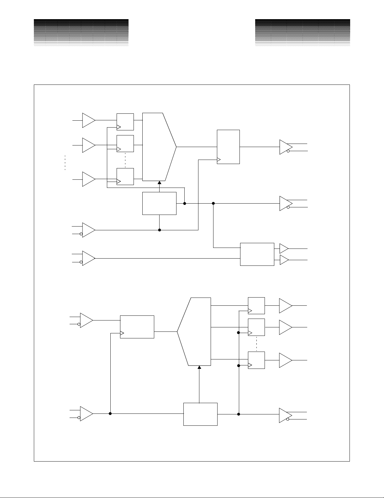
VSC8061 Multiplexer
The VSC8061 consists of a 16:1 multiplexer circuit, a phase detector, and a timing circuit which generates
a divide-by-16 clock from the high-speed clock input. The 16:1 multiplexer accepts 16 parallel single-ended
ECL compatible inputs (D0...D15) at data rates up to 156Mb/s and bitwise serializes them into a 2.5Gb/s serial
output (DO/DON). The internal timing of the VSC8061 is referenced to the negative going edge of the highspeed clock true input (CLK). This clock is divided by 16 and is provided as an output (CLK16/CLK16N). The
setup and hold time of the parallel inputs (D[0:15]) are specified with respect to the falling edge of CLK16, so
that CLK16/CLK16N can be used to clock the data source of D[0:15]. The on-chip phase detector monitors the
phase relationship between the internally generated divide-by-16 clock and an externally supplied low-speed
reference clock input (DCLK/DCLKN). Phase difference between these two clock signals generates an up or
down output (U, D) for phase lock applications. The phase detector can be used as part of an external Phase
Locked Loop (PLL) to implement a clock multiplication function.
In applications where a 2.5GHz system clock is provided, and the phase detector function is not required, it
is recommended to connect one side of the DCLK/DCLKN input to VTT through a 50Ω resistor. The U and D
output can be left open and unused.
VSC8062 Demultiplexer
The VSC8062 consists of a 1:16 demultiplexer and timing circuitry which generates a divide-by-16 clock
from the high-speed clock input. The demultiplexer accepts a serial data stream input (DI/DIN) at up to 2.5Gb/s
and deserializes it into 16 parallel single-ended ECL compatible outputs (D[0:15]) at data rates up to 156 Mb/s.
The internal timing of the VSC8062 is referenced to the negative going edge of the high-speed clock true input
(CLK). This clock is divided by 16 and provided as an output (CLK16/ CLK16N). The timing parameters of the
parallel data outputs (D[0:15]) are specified with respect to the falling edge of CLK16, so that CLK16/CLK16N
can be used to clock the destination of D[0:15].
G52069-0, Rev 4.3 Page 1
05/11/01
© VITESSE SEMICONDUCTOR CORPORATION • 741 Calle Plano • Camarillo, CA 93012
Tel: (800) VITESSE • FAX: (805) 987-5896 • Email: prodinfo@vitesse.com
Internet: www.vitesse.com
Page 2
VITESSE
VSC8061/VSC8062
SEMICONDUCTOR CORPORATION
2.5Gb/s 16-Bit
Multiplexer/Demultiplexer Chipset
Figure 1: VSC8061 Block Diagram
D
0
D
1
Parallel Data
Receivers
D
15
Input
Registers
CLK
CLKN
16:1
Multiplexer
Timing
Generator
Bit Rate Clock
Output
Register
Data Sheet
DO
DON
CLK16
CLK16N
DCLK
DCLKN
DI
DIN
CLK
CLKN
Figure 2: VSC8062 Block Diagram
Input
Register
De-
Multiplexer
1:16
Timing
Generator
Phase
Detector
Output
Registers
D
D
Parallel Data
Outputs
D
CLK16
CLK16N
U
D
0
1
15
Page 2 G52069-0, Rev 4.3
© VITESSE SEMICONDUCTOR CORPORATION • 741 Calle Plano • Camarillo, CA 93012
Tel: (800) VITESSE • FAX: (805) 987-5896 • Email: prodinfo@vitesse.com
Internet: www.vitesse.com
05/11/01
Page 3
VITESSE
SEMICONDUCTOR CORPORATION
VSC8061/VSC8062
Multiplexer/Demultiplexer Chipset
Data Sheet
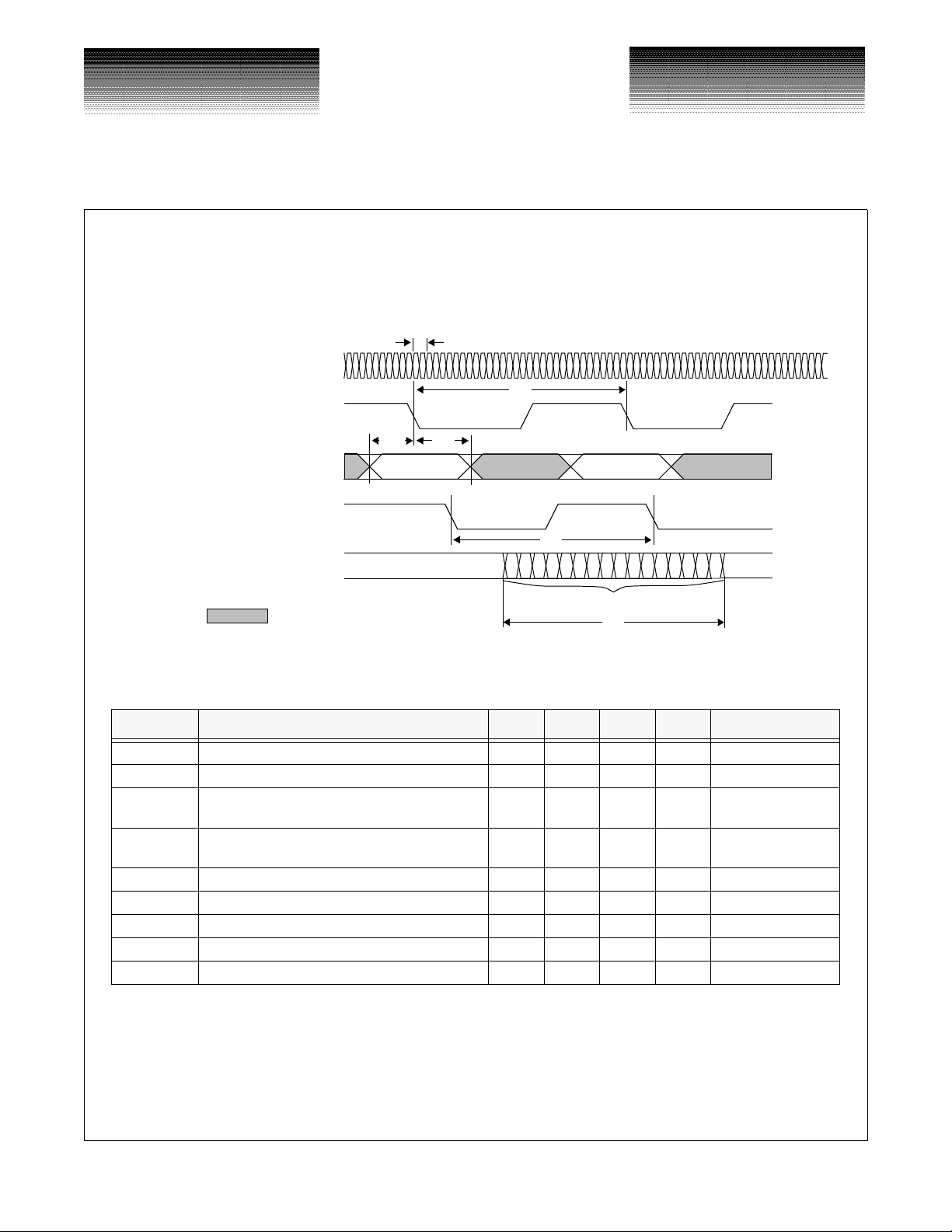
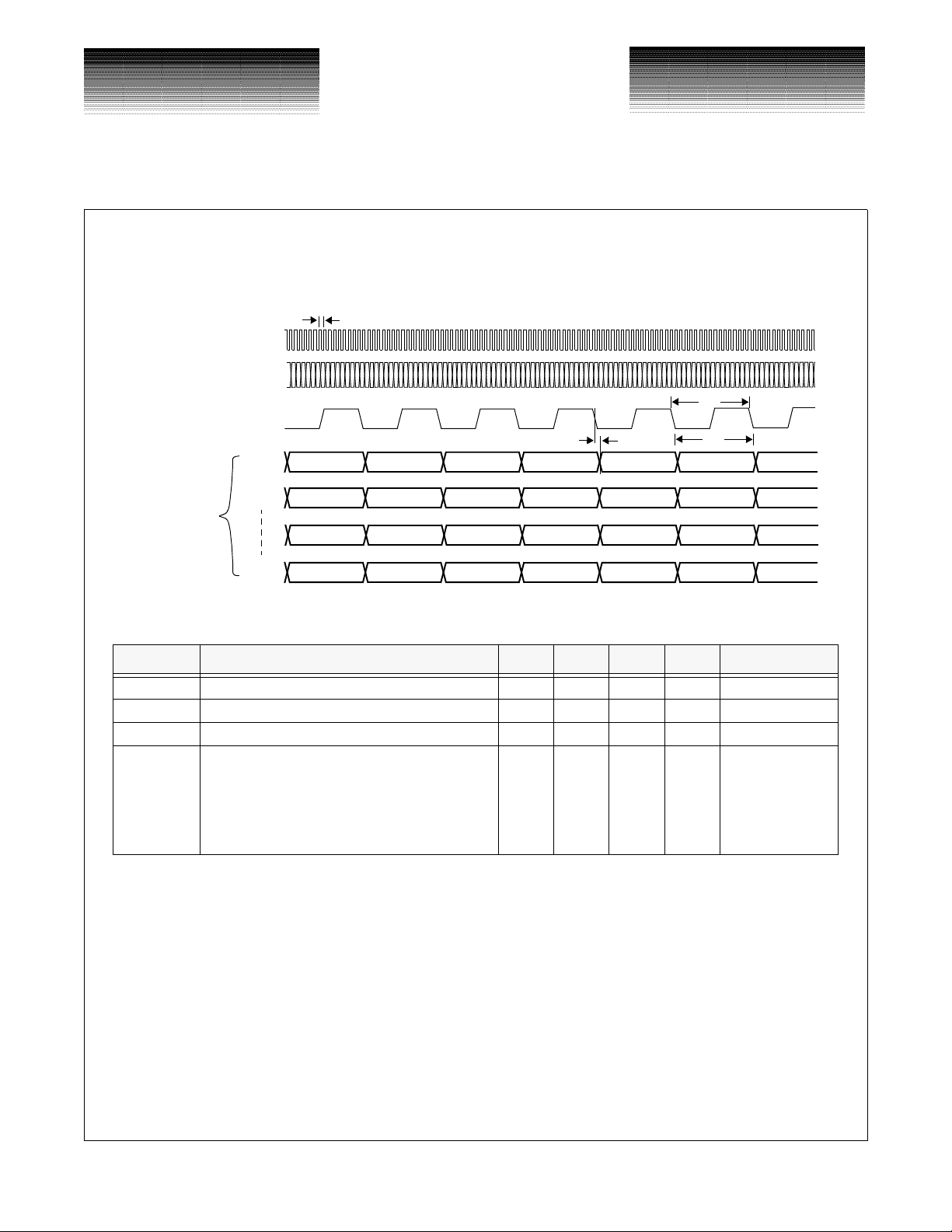
VSC8061 Multiplexer AC Characteristics (Over recommended operating range)
Figure 3: VSC8061 Multiplexer Waveforms
t
CLK
2.5Gb/s 16-Bit
High-speed differential clock input
CLK (CLKN)
t
D
CLK16 (CLK16N)
Parallel data clock output
D[0:15]
Parallel data inputs
t
DSU
VALID DATA (1)
t
DH
VALID DATA (2)
DCLK (DCLKN)
Parallel data clock input
DO (DON)
High-speed differential serial data output
NOTE:
Table 1: VSC8061 AC Characteristics
Parameter Description Min Typ Max Units Conditions
t
CLK
t
D
t
DSU
t
DH
t
DC
tR, t
F
tR, t
F
tR, t
F
tR, t
F
NOTE: (1) Devices are guaranteed to operate to a maximum frequency of 2.5GHz.
Clock period
CLK16, DCLK period (t
Parallel data set-up time with respect to CLK16
falling edge
Data hold time with respect to CLK16 falling
edge
CLK16 duty cycle 40 60 %
DCLK (DCLKN) rise and fall times 1.5 ns 10% to 90%
D[0:15] rise and fall times 2.0 ns 10% to 90%
CLK16 (CLK16N) rise and fall times 0.5 1.0 ns 10% to 90%
DO (DON) rise and fall times 150 165 ps 20% to 80%
=Don’t care
(1)
x 16) 6.4 15.6 ns
CLK
t
D
D0 D1 D2 D3 D4 D5 D6 D7 D8 D9 D10 D11D12 D13 D14 D15
Serialized Data
t
D
400 ps
2.0 ns
0.5 ns
G52069-0, Rev 4.3 Page 3
05/11/01
© VITESSE SEMICONDUCTOR CORPORATION • 741 Calle Plano • Camarillo, CA 93012
Tel: (800) VITESSE • FAX: (805) 987-5896 • Email: prodinfo@vitesse.com
Internet: www.vitesse.com
Page 4
VITESSE
VSC8061/VSC8062
SEMICONDUCTOR CORPORATION
2.5Gb/s 16-Bit
Multiplexer/Demultiplexer Chipset
Data Sheet
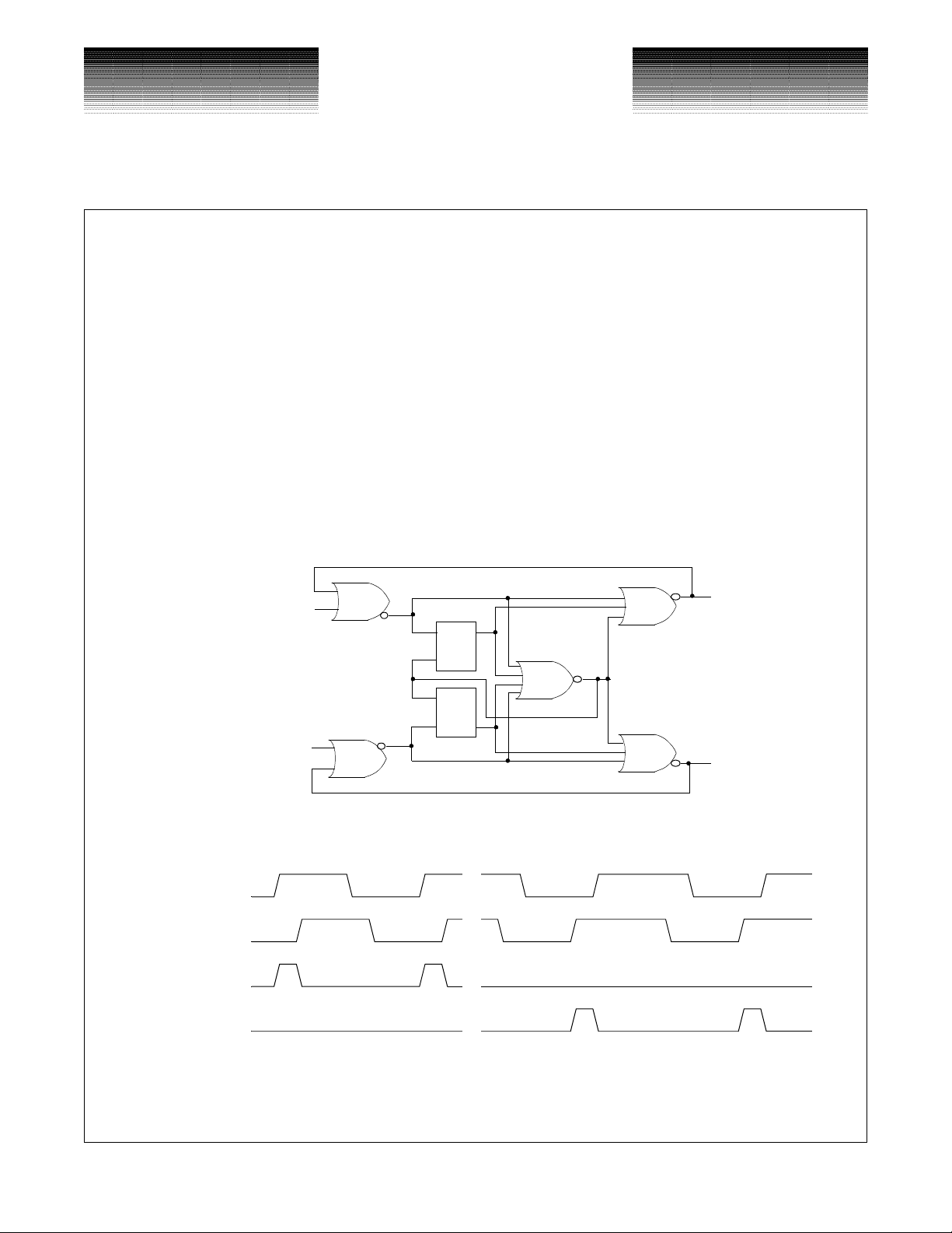
VSC8061 Phase Detector Logic Diagram
The internal phase detector of the VSC8061 compares the phase difference between the internally generated divide-by-16 clock and the DCLK input. If both inputs (CLK16 and DCLK) to the phase detector are in
phase, the U and D outputs will both be low. If the rising edge of CLK16 precedes DCLK, a series of pulses
with pulse widths proportional to the phase difference will be present at the U output. Conversely, if DCLK precedes CLK16, then a series of pulses with widths proportional to the phase difference will be present at the D
output. The other output will remain low. The Phase Detector ignores phase differences for falling edges. This
circuitry is useful for implementing a Clock Multiplier Unit (CMU) function with the VSC8061. For example,
the DLCK can be the system reference clock at the parallel data rate. An external Voltage Controlled Oscillator
(VCO) at 16x the frequency of the reference clock can be used as the CLK input for the VSC8061. The phase
detector outputs (U and D) can then be used by an external integrator to generate an output that controls the
VCO. The generated 16x clock from the VCO will be phase-locked to the reference clock.
Figure 4: VSC8061 Phase Detector Logic Diagram
CLK16
RSQ
U
CLK16
DCLK
S
R Q
DCLK
Figure 5: Phase Detector Input and Output Waveforms
~
~
~
~
U
D
~
~
~
~
D
Page 4 G52069-0, Rev 4.3
© VITESSE SEMICONDUCTOR CORPORATION • 741 Calle Plano • Camarillo, CA 93012
Tel: (800) VITESSE • FAX: (805) 987-5896 • Email: prodinfo@vitesse.com
Internet: www.vitesse.com
05/11/01
Page 5
VITESSE
SEMICONDUCTOR CORPORATION
VSC8061/VSC8062
Multiplexer/Demultiplexer Chipset
Data Sheet
VSC8062 Demultiplexer AC Characteristics (Over recommended operating range)
Figure 6: VSC8062 Timing Diagram
t
High-speed differential clock input
CLK (CLKN)
DI (DIN)
High-speed serial data input
Parallel data clock output
CLK16
D0
D1
CLK
t
D
t
BD
t
D
2.5Gb/s 16-Bit
Data Outputs
Demultiplexed Parallel
D15
Table 2: VSC8062 AC Characteristics
Parameter Description Min Typ Max Units Conditions
t
CLK
t
D
t
DSU
t
DH
NOTES: (1) If t
(2) t
SU
(3) At t
Clock period
BYTE CLK16 period (t
CLK16 falling edge output to valid data 1.0 3.0 ns
Phase Margin =
Serial data phase timing margin with respect to
high-speed clock
changes, all remaining parameters change as indicated by the equations.
CLK
and t
are setup and hold times of the serial data input register.
H
= 400ps.
CLK
(1)
x 16) 6.4 ns
CLK
tSUtH+
1
-------------------–
t
CLK
(2)
360°×
400 ps
(3)
180
degrees
G52069-0, Rev 4.3 Page 5
05/11/01
© VITESSE SEMICONDUCTOR CORPORATION • 741 Calle Plano • Camarillo, CA 93012
Tel: (800) VITESSE • FAX: (805) 987-5896 • Email: prodinfo@vitesse.com
Internet: www.vitesse.com
Page 6
VITESSE
VSC8061/VSC8062
SEMICONDUCTOR CORPORATION
2.5Gb/s 16-Bit
Multiplexer/Demultiplexer Chipset
DC Characteristics
Table 3: ECL Inputs and Outputs
(Over recommended operating conditions with internal V
REF, VCC
Parameter Description Min Typ Max Units Conditions
V
OH
V
OL
V
IH
V
IL
∆VECL
∆VECL
Note: Differential ECL output pins must be terminated identically.
Output HIGH voltage -1100 -700 mV
Output LOW voltage V
Input HIGH voltage -1040 -600 mV
Input LOW voltage V
Output voltage swing 0.850 V Output load 50Ω to V
OUT
Input voltage swing 0.600 0.800 1.2 V AC-coupled
IN
Table 4: Power Dissipation
(Over recommended operating conditions, VCC= GND, outputs open circuit)
= GND, output load = 50Ω to -2.0V).
TT
TT
-1750 mV
-1600 mV
VIN = VIH (max) or VIL
(min)
VIN = VIH (max) or VIL
(min)
Guaranteed HIGH signal
for all inputs
Guaranteed LOW signal
for all inputs
Data Sheet
TT
Parameter Description Min Typ Max Units Conditions
I
EE
I
TT
P
D
Power supply current from V
Power supply current from V
Power dissipation
VSC8061 260 mV
EE
VSC8062 220 mV
VSC8061 260 mV
TT
VSC8062 230 mV
VSC8061 2.0 W
VSC8062 1.7 W
Table 5: High-Speed Input and Output Specifications
(Over recommended operating conditions, VCC = GND, output load = 50Ω to -2.0V)
Parameter Description Min Typ Max Units Conditions
∆V
HSOUT
∆V
HSIN
tR, t
F
NOTES: (1) Built-in references generator, the high-speed inputs are designed for AC-coupling.
Output voltage swing 0.7 0.9 V Output load, 50Ω to -2.0V
Input voltage swing See Table 6 AC-coupled
Same for all data rates; no
Input voltage rise and fall time (high-speed) 0.2 1.5 ns
(2) If a high-speed input is driven single-ended, a capacitor should be connected between the unused high-speed or complement
input and V
(see Figures 7 and 8).
TT
worse than sine wave at
max speed
Page 6 G52069-0, Rev 4.3
© VITESSE SEMICONDUCTOR CORPORATION • 741 Calle Plano • Camarillo, CA 93012
Tel: (800) VITESSE • FAX: (805) 987-5896 • Email: prodinfo@vitesse.com
Internet: www.vitesse.com
05/11/01
Page 7

SEMICONDUCTOR CORPORATION
Data Sheet
VSC8061/VSC8062
Multiplexer/Demultiplexer Chipset
5±5
±
VITESSE
2.5Gb/s 16-Bit
(V
(1)
) ............................................................... VEE-0.7V to V
HSIN
|) can be greater than |V
HSIN
TT
CC
- 0.5V|.
+0.7V
Absolute Maximum Ratings
Power Supply Voltage (VTT) ............................................................................................................-3.0V to 0.5V
Power Supply Voltage (VEE) .................................................................................................VTT + 0.7V to -7.0V
Input Voltage Applied
High-Speed Input Voltage Applied
Output Current, I
Case Temperature Under Bias (TC)................................................................................................ -55oC to 125oC
Storage Temperature (T
NOTES: (1) Caution: Stresses listed under “Absolute Maximum Ratings” may be applied to devices one at a time without causing perma-
nent damage. Functionality at or exceeding the values listed is not implied. Exposure to these values for extended periods may
affect device reliability.
(2) VTT must be applied before the magnitude of any input signal voltage (|VIN|, |V
(2)
(V
(DC, output HI) ........................................................................................................-50mA
OUT
STG
) ..................................................................................................-2.5V to 0.5V
ECLIN
(2)
) .......................................................................................................... -65oC to 150oC
Recommended Operating Conditions
Power Supply Voltage (VTT) .................................................................................................................-2.0V%
Power Supply Voltage (VEE) .................................................................................................................-5.2V%
Operating Temperature Range
NOTE: (1) Lower limit of specification is ambient temperature and upper limit is case temperature.
(1)
(T)............................(Commercial) 0oC to +70oC, (Industrial) -40oC to +85oC
ESD Ratings
For performance considerations, minimum ESD protection is provided for the high-speed input pins. Therefore, proper procedures should be used when handling these products. The VSC8061/8062 are rated to the following ESD voltages based on the human body model:
1. All high-speed input pins are rated at or above 500V.
2. All other pins are rated at or above 2000V.
The above ratings apply to both “F” and “QH” packages.
G52069-0, Rev 4.3 Page 7
05/11/01
© VITESSE SEMICONDUCTOR CORPORATION • 741 Calle Plano • Camarillo, CA 93012
Tel: (800) VITESSE • FAX: (805) 987-5896 • Email: prodinfo@vitesse.com
Internet: www.vitesse.com
Page 8

VITESSE
VSC8061/VSC8062
SEMICONDUCTOR CORPORATION
2.5Gb/s 16-Bit
Multiplexer/Demultiplexer Chipset
Coupling for Inputs
Figure 7: AC-Coupling for DCLK, DCLKN Inputs
Z
O
RT = Z
C
IN
O
V
TT
C
SE
V
TT
Chip Boundary
DCLK
DCLKN
-1.32V
VCC = GND
VTT = -2V
-1.32V
R
| |
Data Sheet
= 1kΩ
CIN typ = 0.1µF
CSE typ = 0.1µF for single-ended applications
(Capacitor values are selected for DCLK = 155Mb/s.)
DCLK, DCLKN Inputs
Internal biasing will position the reference voltage of approximately -1.32V on both the true and complement inputs. This input can either be DC-coupled or AC-coupled; it can also be driven single-ended or differentially. Figure 7 shows the configuration for a single-ended, AC-coupling operation. In the case of direct
coupling and single-ended input, it is recommended that a stable V
for ECL levels be used for the comple-
REF
mentary input.
High-Speed Clock and Serial Data Inputs
It is recommended that all high-speed clock and serial data inputs (CLK/CLKN for the VSC8061; DI/DIN
and CLK/CLKN for the VSC8062) be AC-coupled. Figure 8 shows the configuration for a single-ended ACcoupling operation.
In most situations, these inputs will have high transition density and little DC offset. However, in cases
where this does not hold, direct DC connection is possible. The following is to assist in this application.
All serial data and clock inputs have the same circuit topology, as shown in Figure 8. The reference voltage
is created by a resistor divider as shown. If the input signal is driven differentially and DC-coupled to the part,
the mid-point of the input signal swing should be centered about this reference voltage and not exceed the maximum allowable amplitude. For single-ended, DC-coupling operations, it is recommended the user provide an
external reference voltage which has better temperature and power supply noise rejection than the on-chip resistor divider. The external reference should have a nominal value as indicated in the table and can be connected to
either side of the differential gate.
Page 8 G52069-0, Rev 4.3
© VITESSE SEMICONDUCTOR CORPORATION • 741 Calle Plano • Camarillo, CA 93012
Tel: (800) VITESSE • FAX: (805) 987-5896 • Email: prodinfo@vitesse.com
Internet: www.vitesse.com
05/11/01
Page 9

VITESSE
SEMICONDUCTOR CORPORATION
VSC8061/VSC8062
Multiplexer/Demultiplexer Chipset
Data Sheet
Table 6: High-Speed Clock and Serial Data Inputs
Product Input Reference Min (p-p) Max (p-p)
VSC8061 DCLK, DCLKN -1.32V 600mV 1.2V
VSC8061 CLK, CLKN -3.5V 600mV 1.2V
VSC8062 DI, DIN -3.5V 250mV 1.2V
VSC8062 CLK, CLKN -3.5V 250mV 1.2V
Figure 8: High-Speed Clock and Serial Data Inputs
Chip Boundary
VCC = GND
2.5Gb/s 16-Bit
Z
O
RT = Z
CIN typ = 100pF
CSE typ = 100pF for single-ended applications
(Capacitor values are selected for DI = 2.5Gb/s.)
C
IN
CLK,
DI
O
V
TT
C
SE
CLKN,
DIN
V
TT
-3.5V
VEE = -5.2V
-3.5V
R
= 1.3kΩ
| |
G52069-0, Rev 4.3 Page 9
05/11/01
© VITESSE SEMICONDUCTOR CORPORATION • 741 Calle Plano • Camarillo, CA 93012
Tel: (800) VITESSE • FAX: (805) 987-5896 • Email: prodinfo@vitesse.com
Internet: www.vitesse.com
Page 10

VITESSE
VSC8061/VSC8062
SEMICONDUCTOR CORPORATION
2.5Gb/s 16-Bit
Multiplexer/Demultiplexer Chipset
Package Pin Descriptions
Figure 9: VSC8061/8062 F (52-Pin LDCC) Pin Diagrams
Heat Sink Up
Top View
D2
D3
D4
VCC
D5
D6
VTT
D7
D8
VCC
D9
D10
NC
D1D0NC
VCC
DCLKN
DCLK
VEEDU
VCCNCTEST
39383736353433323130292827
40
41
42
43
44
45
46
47
VSC8061
Heat Sink Side
48
49
50
51
52
1 2 3 4 5 6 7 8 9 10111213
TEST
26
25
24
23
22
21
20
19
18
17
16
15
14
Data Sheet
NC
NC
NC
VEE*
NC
NC
NC
DO
VCC
DON
NC
NC
NC
D11
D12
D11NCNC
D13
D14
D15
VCC
VCC
VTT
CLK16N
D12
D13
VEE
D14
NC
VCC
CLK16
D15
VCCNCTEST
CLK
CLKN
TEST
39383736353433323130292827
D10
D9
D8
VCC
D7
D6
VTT
D5
D4
VCC
D3
D2
NC
40
41
42
43
44
45
46
47
VSC8062
Heat Sink Side
48
49
50
51
52
1 2 3 4 5 6 7 8 9 10111213
D1
NC
NC
D0
VCC
CLK16N
NC
VTT
VCC
CLK16
26
25
24
23
22
21
20
19
18
17
16
15
14
NCNCNC
*Heat sink is electrically connected to pin 23 and should be biased to VEE.
NC
NC
NC
VEE*
NC
CLK
CLKN
DIN
VCC
DI
NC
NC
NC
Page 10 G52069-0, Rev 4.3
© VITESSE SEMICONDUCTOR CORPORATION • 741 Calle Plano • Camarillo, CA 93012
Tel: (800) VITESSE • FAX: (805) 987-5896 • Email: prodinfo@vitesse.com
Internet: www.vitesse.com
05/11/01
Page 11

SEMICONDUCTOR CORPORATION
Data Sheet
VSC8061/VSC8062
Multiplexer/Demultiplexer Chipset
Heat Spreader Up
Top View
VITESSE
Figure 10: VSC8061/8062 QH (52-Pin PQFP) Pin Diagrams
VEE*
VCC
VEE
VEE
DON
VEE
NC
VEE
NC
VCC
CLK
CLKN
VEE
VTT
CLK16
CLK16N
D15
D14
D13
D12
D11
VCC
VCC
VTT
TEST
TEST
VTT
NC
DCLK
DCLKN
D0
VCC
VTT
NC
NC
NC
DO
52
1
VITESSE
U
D
VSC8061QH
2.5Gb/s 16-Bit
VCC
VTT
NC
TEST
VTT
NC
TEST
D15
D14
D13
D12
VCC
VTT
52
1
1
D1D2D3D4D5
VTT
VEE*
VCCNCVEE
CLK
VITESSE
VSC8062QH
D9D8D7
D11
D10
VTT
D6
D7D8D9
D5D4D3
D10
VEENCNC
D2
VTT
VCC
NC
NC
VEE
VTT
NC
NC
NC
CLK16
CLK16N
D0
D1
VCC
VTT
VTT
CLKN
VEE
DINDIVEE
D6
VTT
*Heat spreader is electrically connected to pin 52 and should be biased to VEE.
G52069-0, Rev 4.3 Page 11
05/11/01
© VITESSE SEMICONDUCTOR CORPORATION • 741 Calle Plano • Camarillo, CA 93012
Tel: (800) VITESSE • FAX: (805) 987-5896 • Email: prodinfo@vitesse.com
Internet: www.vitesse.com
Page 12

VITESSE
VSC8061/VSC8062
SEMICONDUCTOR CORPORATION
2.5Gb/s 16-Bit
Multiplexer/Demultiplexer Chipset
Table 7: VSC8061 Pin Identifications
Pin Number
QH Package
38 13 CLK I HS High-speed clock true
37 12 CLKN I HS High-speed clock, complement
9 34 DCLK I ECL Data clock true
10 35 DCLKN I ECL Data Clock complement
34 9 CLK16 O ECL Clock divide-by-16, true
33 8 CLK16N O ECL Clock divide-by-16, complement
11, 15-20, 22-
25, 28-32
45 19 DO O HS Serial data output, true
44 17 DON O HS Serial data output, complement
7 31 U O ECL Phase detector output - up frequency
8 32 D O ECL Phase detector output - down frequency
1, 12, 27,
39, 51
2, 5, 13, 14, 21,
26, 35
36, 42, 43,
46, 49
6, 40, 41, 47,
48, 50
3, 4 27, 28 Test
52 23 V
NOTE: (1) Can be used single-ended.
Pin number
F Package
1-3, 5, 6,
8-42, 44, 45,
47, 48, 50, 51
4, 10, 18, 30,
36, 43, 49
7,46 V
33 V
11, 14-16,
20-22, 24-26,
29, 37, 52
Signal
Name
D[0:15] I ECL Parallel data inputs
V
I/O Level Description
(1)
(1)
(1)
CC
TT
EE
NC Do not connect, leave open
EE
Pwr Most positive power supply
Pwr DCFL negative power supply
Pwr SCFL negative power supply
Test inputs. Used in factory for testing, connect to
VTT through a resistor
Pwr Heat sink bias, connect to V
Data Sheet
(1)
EE
Page 12 G52069-0, Rev 4.3
© VITESSE SEMICONDUCTOR CORPORATION • 741 Calle Plano • Camarillo, CA 93012
Tel: (800) VITESSE • FAX: (805) 987-5896 • Email: prodinfo@vitesse.com
Internet: www.vitesse.com
05/11/01
Page 13

SEMICONDUCTOR CORPORATION
Data Sheet
VSC8061/VSC8062
Multiplexer/Demultiplexer Chipset
Table 8: VSC8062 Pin Identifications
VITESSE
2.5Gb/s 16-Bit
Pin Number
QH Package
48 21 CLK I HS High-speed clock, true
47 20 CLKN I HS High-speed clock, complement
44 17 DI I HS Serial data input, true
45 19 DIN I HS Serial data input, complement
31 8 CLK16 O ECL
30 6 CLK16N O ECL
8-11, 15-20,
22-25, 28, 29
1, 12, 27,
39, 51
2, 5, 13, 14, 21,
26, 35
36, 42, 43,
46, 49
3, 6, 32-34, 37,
38, 40, 41, 50
4, 7 28, 29 Test Pwr
52 23 V
NOTE: (1) Can be used single-ended.
Pin Number
F Package
3, 5, 31, 32,
34, 35, 39-42,
44, 45, 47, 48,
50, 51
4, 10, 18, 30,
36, 43, 49
7, 46 V
33 V
1, 2, 9, 11-16,
22, 24-27, 37,
38, 52
Signal
Name
D[0:15] O ECL Parallel data outputs
V
CC
TT
EE
NC Do not connect, leave open
EE*
I/O Level Description
Parallel data clock (high-speed clock divide-by-
16), true
Parallel data clock (high-speed clock divide-by-
16), complement
Pwr Most positive power supply
Pwr DCFL negative power supply
Pwr SCFL negative power supply
Test inputs. Used in factory for testing, connect
to VTT through a resistor
Pwr
Heat sink bias, connect to V
(1)
(1)
EE
(1)
(1)
G52069-0, Rev 4.3 Page 13
05/11/01
© VITESSE SEMICONDUCTOR CORPORATION • 741 Calle Plano • Camarillo, CA 93012
Tel: (800) VITESSE • FAX: (805) 987-5896 • Email: prodinfo@vitesse.com
Internet: www.vitesse.com
Page 14

VITESSE
VSC8061/VSC8062
SEMICONDUCTOR CORPORATION
2.5Gb/s 16-Bit
Multiplexer/Demultiplexer Chipset
Package Information
B
HEAT SINK SIDE
PACKAGE IS
CAVITY DOWN
52
1
o
E
45
N
O
52-Pin Ceramic LDCC (F) Package
K
L
D
NOTES:
Drawing not to scale.
All units in mm unless otherwise noted.
Packages: Ceramic (alumnia)
Heat Sinks: Copper tungsten
Leads: Alloy 42 with gold plating
A
C
M
Data Sheet
I
J
Item mm (Min/Max) in (Min/Max) Item mm (Min/Max) in (Min/Max)
A 18.54/19.56 0.730/0.770 I 0.41/0.61 0.016/0.024
B 1.02/1.52 0.040/0.060 J 2.03/2.79 0.080/0.110
(1)
C
(1)
D
E 1.27 TYP 0.050 TYP M 27.69/30.22 1.090/1.190
NOTE: (1) At package body.
15.49/16.51 0.610/0.650 K
15.24 TYP 0.600 TYP L 4.57/5.34 0.180/0.210
(1)
N 0.36/0.56 0.014/0.022
O 1.75/1.90 0.069/0.075
0.09/0.24 0.003/0.009
Page 14 G52069-0, Rev 4.3
© VITESSE SEMICONDUCTOR CORPORATION • 741 Calle Plano • Camarillo, CA 93012
Tel: (800) VITESSE • FAX: (805) 987-5896 • Email: prodinfo@vitesse.com
Internet: www.vitesse.com
05/11/01
Page 15

SEMICONDUCTOR CORPORATION
Data Sheet
VSC8061/VSC8062
Multiplexer/Demultiplexer Chipset
VITESSE
2.5Gb/s 16-Bit
52 Pin PQFP (QH) Package
F
G
52 40
Item mm Tol.
A 2.35 MAX
1
39
D 2.00 +.10 / -.05
E 0.35 ±.05
F 17.20 ±.25
G 14.00 ±.10
L
I H
H 17.20 ±.25
I 14.00 ±.10
J 0.88 +.15 / -.10
13
27
J1 0.80 +.15 / -.10
K 1.00 BASIC
2614
10o TYP
A
L 5.84 ±.50 DIA.
D
0.30 RAD. TYP.
0.20 RAD. TYP.
NOTES:
Drawing not to scale.
Heat spreader up.
All units in mm unless otherwise noted.
G52069-0, Rev 4.3 Page 15
05/11/01
© VITESSE SEMICONDUCTOR CORPORATION • 741 Calle Plano • Camarillo, CA 93012
100 TYP
A
0.17 MAX.
Tel: (800) VITESSE • FAX: (805) 987-5896 • Email: prodinfo@vitesse.com
0.25
K
0o- 8o
J
1
J
Internet: www.vitesse.com
STANDOFF
E
0.25 MAX.
0.102 MAX. LEAD
COPLANARITY
Page 16

VITESSE
VSC8061/VSC8062
SEMICONDUCTOR CORPORATION
2.5Gb/s 16-Bit
Data Sheet
Multiplexer/Demultiplexer Chipset
Thermal Considerations
The VSC8061 and VSC8062 are available in ceramic LDCC and thermally enhanced plastic quad flatpacks. These packages have been enhanced to improve thermal dissipation through low thermal resistance paths
from the die to the exposed surface of the heat spreader. The thermal resistance of the two packages is shown in
the following table
Table 9: Thermal Resistance
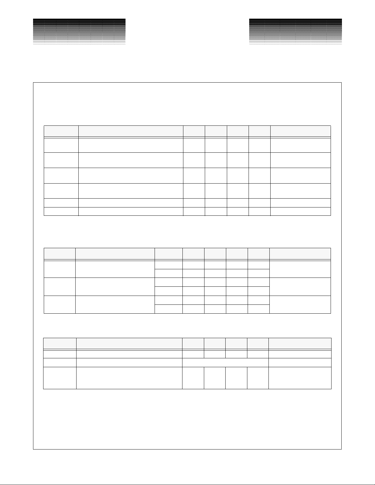
Symbol Description F Pack QH Pack Units
θ
JC
θ
CA
Thermal Resistance with Airflow
Shown in Table 10 is the thermal resistance with airflow. This thermal resistance value reflects all the thermal paths including through the leads in an environment where the leads are exposed. The temperature difference between the ambient airflow temperature and the case temperature should be the worst case power of the
device multiplied by the thermal resistance.
Thermal resistance from junction-to -case. 1.3 2.1 °C/W
Thermal resistance from case-to-ambient still air including
conduction through the leads.
18.5 30.0
°C/W
Table 10: Thermal Resistance with Airflow
Airflow θCA for F Package θCA for QH Package Units
100 lfpm 15.9 24
200 lfpm 14.9 21
300 lfpm 14.2 19
500 lfpm 13.3 15
Thermal Resistance with Heat Sink
The determination of appropriate heat sink to use is as shown below, using the VSC8061 in QH package as
an example.
Figure 11: VSC8061 in QH Package
T
A
θ
SA
θ
CS
o
C/W
o
C/W
o
C/W
o
C/W
Page 16 G52069-0, Rev 4.3
© VITESSE SEMICONDUCTOR CORPORATION • 741 Calle Plano • Camarillo, CA 93012
Tel: (800) VITESSE • FAX: (805) 987-5896 • Email: prodinfo@vitesse.com
Internet: www.vitesse.com
05/11/01
Page 17

SEMICONDUCTOR CORPORATION
Data Sheet
VSC8061/VSC8062
Multiplexer/Demultiplexer Chipset
SA
The worst-case temperature rise from case to ambient is given by the equation:
VITESSE
2.5Gb/s 16-Bit
where:
θ
SA
θ
CS
Τ
A(MAX)
Τ
C(MAX)
∆T = TC - T
P
(MAX)
= Theta sink-to-ambient
= Theta case-to-sink
= Air temperature, user supplied (typically +55o C)
= Case temperature (+85oC for Industrial range)
= Power (2.0 W for VSC8061)
∆TP
A
MAX()θSAθCS
∆T
P∴
-------
Σθ
θ
SA
∆T
------- θCS–=
P
+()=
TCTA–
---------------------------==
θ
+
SAθCS
Ιf T
= 55o C and θCS (user supplied) is typically 0.6o C/W,
A
Therefore, to maintain the proper case and junction temperature, a heat sink with a θSA of 14.4oC/W or less
must be selected at the appropriate air flow.
NOTE: The heat spreader is tied to V
G52069-0, Rev 4.3 Page 17
05/11/01
© VITESSE SEMICONDUCTOR CORPORATION • 741 Calle Plano • Camarillo, CA 93012
θ
SA
Tel: (800) VITESSE • FAX: (805) 987-5896 • Email: prodinfo@vitesse.com
8555–()°C
-----------------------------0.6°CW⁄–=
2W
θ
in both the VSC8061 and VSC8062.
EE
Internet: www.vitesse.com
14.4°CW⁄=
Page 18

VITESSE
VSC8061/VSC8062
SEMICONDUCTOR CORPORATION
2.5Gb/s 16-Bit
Multiplexer/Demultiplexer Chipset
Figure 12: Data Eye From Serial Output of VSC8061 in QH Package (D0/D0N)
Data Sheet
Amplitude: 200 mV/div
Time Scale: 50 ps/div
Data Rate: 2.5 Gb/s
2.5Gb/s
231 - 1 PRB Data
1:16
De-serializer
Figure 13: Measurement Setup
16 Channels
at 155Mb/s
D0
D1
D15
D0
D1
VSC8061
D15
Bit Error
Rate Tester
D0
D0N
TEK CSA803
Signal Analyzer
Page 18 G52069-0, Rev 4.3
© VITESSE SEMICONDUCTOR CORPORATION • 741 Calle Plano • Camarillo, CA 93012
Tel: (800) VITESSE • FAX: (805) 987-5896 • Email: prodinfo@vitesse.com
Internet: www.vitesse.com
05/11/01
Page 19

SEMICONDUCTOR CORPORATION
Data Sheet
VSC8061/VSC8062
Multiplexer/Demultiplexer Chipset
Ordering Information
The order number for this product is formed by a combination of the device number, package type, and the
operating temperature range.
VITESSE
2.5Gb/s 16-Bit
VSC80XX
Device Type
VSC8061: 2.5Gb/s 16-bit Multiplexer
VSC8062: 2.5Gb/s 16-bit Demultiplexer
FC
Package and Temperature
FC: 52 Pin Ceramic Leaded Chip Carrier (LDCC),
0°C ambient to +70°C case
FI: 52 Pin Ceramic Leaded Chip Carrier (LDCC),
-40°C ambient to +85°C case
QH: 52-Pin Plastic Flat Quad Pack (PFQP),
0°C ambient to +85°C case
Notice
Vitesse Semiconductor Corporation (“Vitesse”) provides this document for informational purposes only. All information in this document, including descriptions of features, functions, performance, technical specifications and availability, is subject to change without notice at any time. Nothing contained in this document shall be construed as extending any warranty or promise, express or implied, that any Vitesse product will be
available as described or will be suitable for or will accomplish any particular task.
Vitesse products are not intended for use in life support appliances, devices or systems. Use of a Vitesse product in such applications without written consent is prohibited.
G52069-0, Rev 4.3 Page 19
05/11/01
© VITESSE SEMICONDUCTOR CORPORATION • 741 Calle Plano • Camarillo, CA 93012
Tel: (800) VITESSE • FAX: (805) 987-5896 • Email: prodinfo@vitesse.com
Internet: www.vitesse.com
Page 20

VITESSE
VSC8061/VSC8062
SEMICONDUCTOR CORPORATION
2.5Gb/s 16-Bit
Multiplexer/Demultiplexer Chipset
Data Sheet
Page 20 G52069-0, Rev 4.3
© VITESSE SEMICONDUCTOR CORPORATION • 741 Calle Plano • Camarillo, CA 93012
Tel: (800) VITESSE • FAX: (805) 987-5896 • Email: prodinfo@vitesse.com
Internet: www.vitesse.com
05/11/01
 Loading...