

Page 1

Data Sheet
VSC8021/VSC8022
Features
• Serial Data Rates up to 2.5Gb/s
VITESSE
SEMICONDUCTOR CORPORATION
2.5Gb/s SONET-Compatible
8-Bit MUX/DEMUX Chipset
• Differential or Single-Ended Inputs and Outputs
• Parallel Data Rates up to 312.5Mb/s
• ECL 100K Compatible Parallel Data I/Os
• Divide-by-8 Clock for Synchronization of
Parallel Data to Interfacing Chips
• SONET Frame Recovery Circuitry
(VSC8022)
• Compatible with STS-3 to STS-48
SONET Applications
• Low Power Dissipation: 2.3W (Typ Per Chip)
• Standard ECL Power Supplies:
V
= -5.2V, VTT = -2.0V
EE
• Available in Commercial (0
(-40
°C to +85°C) Temperature Ranges
• Proven E/D Mode GaAs Technology
• 52-Pin Leaded Ceramic Chip Carrier
°C to +70°C) or Industrial
Functional Description
The VSC8021 and VSC8022 are high-speed SONET interface devices capable of handling serial data at
rates up to 2.5Gb/s. These devices can be used for STS-3 through STS-48 SONET applications.
These products are fabricated in gall ium arsenide usi ng the Vitesse H-GaAs
achieves high-speed and low power dissipation. These products are packaged in a ceramic 52-pin leaded
ceramic chip carrier.
E/D MESFET process which
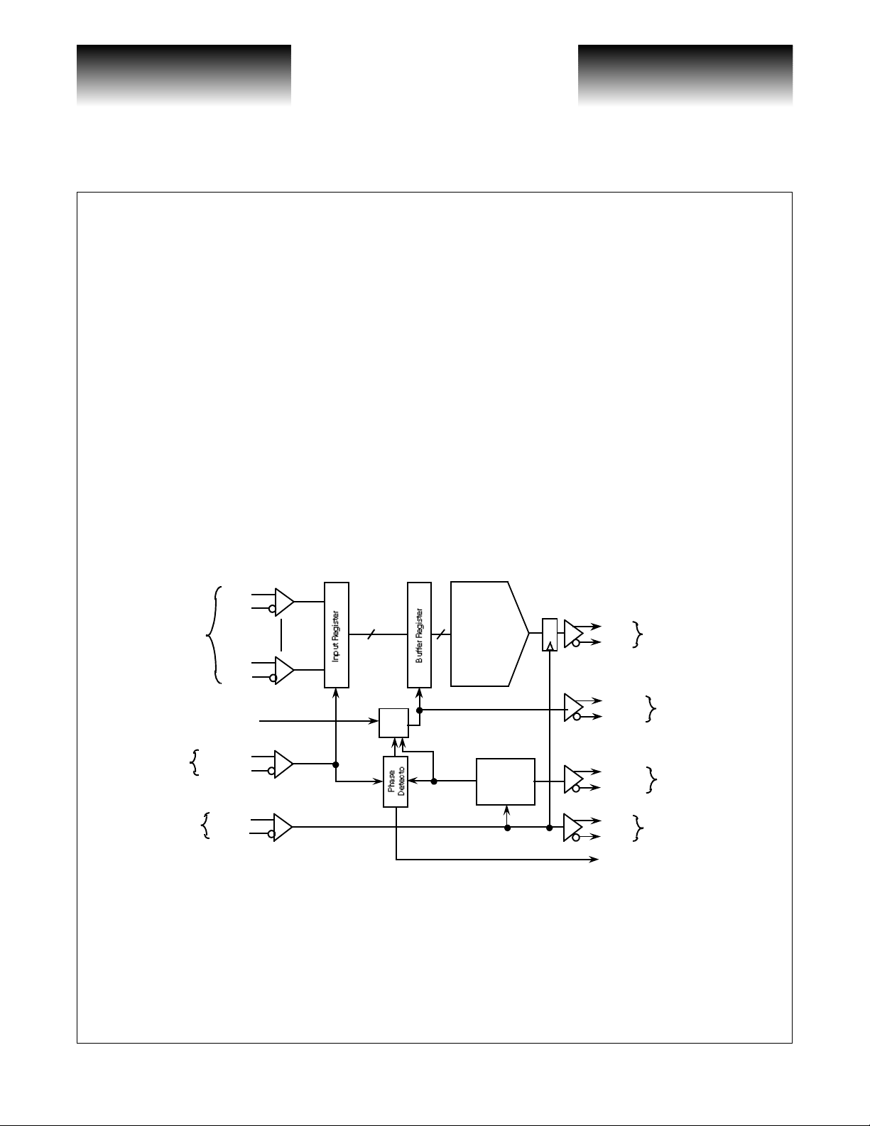
VSC8021
The VSC8021 contain s an 8: 1 multiplexer and a self-positioni ng t ime r. The 8:1 multip lex er ac cept s 8 parallel differential ECL data inputs (D1-D8, D1N-D8N) at rates up to 312.5Mb/s and multiplexes them into a serial
differential bit stream output (DO, DON) at rates up to 2.5Gb/s.
The internal timing of the VSC8021 is built around the high-speed clock (up to 2.5GHz) delivered onto the
chip through a differential input (CLKI, CLKIN). Thi s si gnal i s subsequently echoed at the high-speed differential output (CO, CON).
The parallel data inputs are clocked to on-chip input registers with an externally supplied differential ECL
input (BYCLK, BYCLKN) operating at the same rate as the data inputs. An internal byte clock, which is a
divide-by-8 version of the high-speed clock, is used to transfer the data to a set of buffer registers. This internal
byte clock is brought off chip at the ECL output CLK8, CLK8N.
Internal circuitry monitors the in ternal and ext ernal byte cloc ks and gene rates an ERR sign al if a timing
violation is detected. Thi s sign al ca n be gated to the SYNC input which is edge sensitive high. An active SYNC
input allows the VSC8021 timing to shift, positioning it properly against the external byte clock, CLK8,
CLK8N. When a CLK8 timing switch is made, normal data flow will be invalid for 1 byte.
There are two clock inputs, CLKI and BYCLK, going into the VSC8021. These two clocks serve as timing
references for different parts of the VSC8021. The BYCLK is used to trigger the input registers for the parallel
data inputs, while the CLKI is used to trigger the high-speed serial output register as well as some of the timing
circuitry for the parallel to serial conversion. Furthermore, in order to make this part easy to use, the user is not
required to assume a known phase relationship between CLKI and the BYCLK.
G52028-0, Rev 4.1 Page 1
05/25/01
© VITESSE SEMICONDUCTOR CORPORATION • 741 Calle Plano • Camarillo, CA 93012
Tel: (800) VITESSE • FAX: (805) 987-5896 • Email: prodinfo@vitesse.com
Internet: www.vitesse.com
Page 2
VITESSE
Phase
Adjust
SEMICONDUCTOR CORPORATION
2.5Gb/s SONET-Compatible
8-Bit MUX/DEMUX Chipset
VSC8021/VSC8022
Data Sheet
An internal Phase Detector and Phase Adjust Circuit are used to facilitate the two asynchronous circuits to
work with each other. The Phase Detector and the Phase Adjust Circuit work together to adjust the internal
clock CLK8 to make sure the set up and hold conditions are met for the inter nal regi sters. CLK8 is derived from
CLKI and the RCLK is a non-phase varying byte clo ck output. The edge sensitiv e SYNC signal is simply the
control signal that enables the Phase Detector circuitry.
As a summary, the CLKI is the high-speed clock input. The BYCLK is the external byte clock. The CLK8
is the internal byte clock deriv ed from C LKI, phase-adjusted if SYNC is enabled. The RCLK is a no n-phaseadjusted divided-by-8 clock generated from CLKI. The phase of RCLK, RCLKN is not affected by the selfadjusting circuitry, therefore it can be used as a system reference cl ock . RCLK, RCLKN can be use d by the system designer to generate BYCLK, BYCLKN. The self-posit i oni ng timer and R CLK, RCLKN allow for the creation of very tight parallel data timing for the VSC8021.
Figure 1: VSC8021 Block Diagram
Parallel
Byte Clock
Inputs
High Speed
Clock Inputs
Data
D1N
D8N
SYNC
BYCLK
BYCLKN
CLKI
CLKIN
D1
D8
8 8
8:1
Multiplexer
Timing
Generator
DO
DON
CLK8
CLK8N
RCLK
RCLKN
CO
CON
ERR
Serial Data Output
Phase Adjustable
Byte Clock Output
Independent
Byte Clock Output
High Speed
Clock
Page 2 G52028-0, Rev 4.1
© VITESSE SEMICONDUCTOR CORPORATION • 741 Ca l le Pl an o • Camarillo, CA 93012
Tel: (800) VITESSE • FAX: (805) 987-5896 • Email: prodinfo@vitesse.com
Internet: www.vitesse.com
05/25/01
Page 3
VITESSE
Frame Recovery Disable —
Frame Recovery Clock —
SEMICONDUCTOR CORPORATION
Data Sheet
2.5Gb/s SONET-Compatible
VSC8021/VSC8022
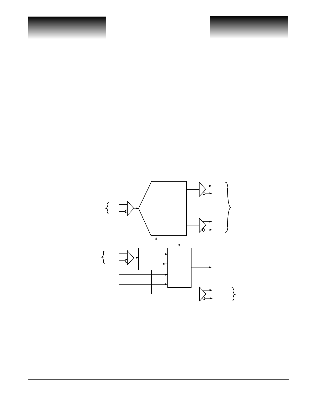
VSC8022
The VSC8022 cont ains bot h a 1:8 demu ltiplex er and SON ET frame re covery c ircuitry. The 1:8 demult iplexer
accepts a serial data input (
(
D1-D8, D1N-D8N) at rates up to 312.5Mb/s. Valid parallel data outputs are indicated by the divide by 8 differential
clock outputs
The VSC8022 also contains a SONET frame recovery circuit. The frame recovery circuits are enabled by a falling edge on the
ing for the SONET framing sequence. Once the frame is detected, the word boundary is realigned, a confirmation
signal is sent off-chip through the
aligner is hunting for the frame,
BYCKO, BYCKON.
OOFN ECL input when the FDIS input is low. Once enabled, the frame recovery circuit starts look-
DI, DIN) at rates up to 2.5Gb/s and converts it into 8 parallel differential ECL data outputs
FP ECL output and the frame rec overy circuits are di sabled. While the fra me
BYCKO, BYCKON and parallel data are invalid.
Figure 2: VSC8022 Block Diagram
8-Bit MUX/DEMUX Chipset
D1
D1N
Serial Data In
High Speed
Clock Inputs
Frame recovery circuits are disabled by frame detection (resulting in FP) or by a falling edge on the OOFN
input while FDIS is high.
DIN
CLKI
CLKIN
FDIS
OOFN
DI
Generator
Demultiplexer
Timing
1:8
SONET
Frame
Detection &
Recovery
Parallel
Data Outputs
D8
D8N
— Frame Detect i on S i gnal
FP
BYCKO
BYCKON
Byte Clock Out
G52028-0, Rev 4.1 Page 3
05/25/01
© VITESSE SEMICONDUCTOR CORPORATION • 741 Calle Plano • Camarillo, CA 93012
Tel: (800) VITESSE • FAX: (805) 987-5896 • Email: prodinfo@vitesse.com
Internet: www.vitesse.com
Page 4
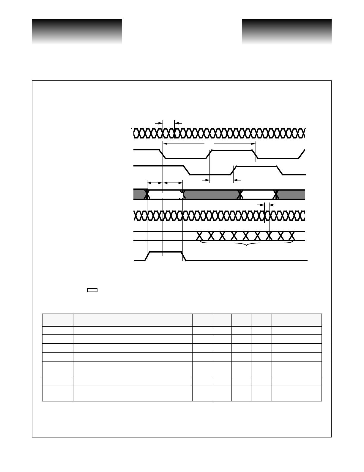
VITESSE
t
C
t
DH
CO, CON
DO,DON
Byte clock input
Parallel differential data inputs
CLK8 adjustment input
Phase adjustable ÷8 output
SEMICONDUCTOR CORPORATION
2.5Gb/s SONET-Compatible
8-Bit MUX/DEMUX Chipset
VSC8021/VSC8022
VSC8021 Multiplexer AC Characteristics (Over recommended operating conditions)
Figure 3: VSC8021 Multiplexer Waveforms
(1)
CLKI , CLKIN
High speed differential clock input
BYCLK (BYCLKN)
(1)
CLK8
D1-D8, D1N-D8N
High speed differential clock outputs
(2)
t
DSU
VALID DATA(1)
t
D
t
BCLK8
VALID DATA(2)
t
CMD
Data Sheet
High speed differential data outputs
SYNC
(1) Negative edge is active edge.
NOTES:
(2) BYCLK/CLK8 timing required when SYNC not connected to ERR.
period x 8 = period.CLKI (CLKIN) BYCLK (BYCLKN)
= Don’t care.
T able 1: VSC8021 Multiplexer AC Characteristics
(over recommended operating conditions)
D01 D02 D03 D04 D05 D06 D07 D08
Serialized Byte 1
Parameter Description Min Typ Max Units Conditions
t
C
t
D
t
DSU
t
DH
t
CMD
t
BCLK8
Jitter (p-p)
NOTES: (1) The parts are guaranteed by design to operate from DC to a maxim um f requency of 2.5GHz.
Clock period
BYTE clock period (tD = tC x 8) 3.2 ns
Parallel data set-up time 0.6 ns
Data hold time 1.4 ns
High-speed clock output (CO, CON) timing, falling
edge of CO to muxed data output, (DO, DON) timing
Byte clock to CLK8 timing
CLKI, CLKIN to DO, DON (max-min), (HI to LO),
same part, same pin at constant conditions
(2) Required when SYNC not connected to ERR.
(1)
(2)
400 ps
220 350 ps
0.5 1.0 1.5 ns
<50 ps
Page 4 G52028-0, Rev 4.1
© VITESSE SEMICONDUCTOR CORPORATION • 741 Ca l le Pl an o • Camarillo, CA 93012
Tel: (800) VITESSE • FAX: (805) 987-5896 • Email: prodinfo@vitesse.com
Internet: www.vitesse.com
05/25/01
Page 5
05/25/01
Tel: (800) VITESSE • FAX: (805) 987-5896 • Email: prodinfo@vitesse.com
G52028-0, Rev 4.1 Page 5
© VITESSE SEMICONDUCTOR CORPORATION • 741 Calle Plano • Camarillo, CA 93012
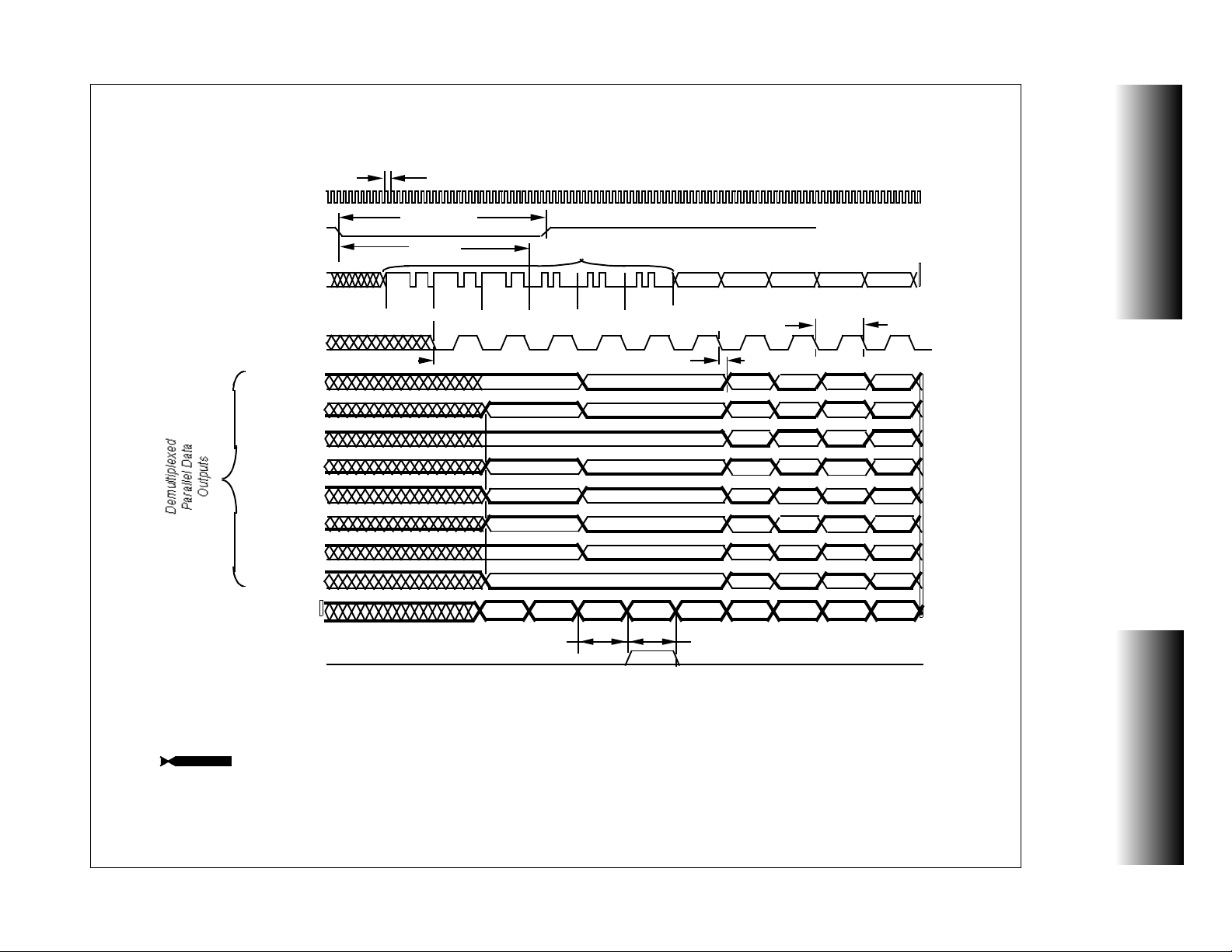
(1)
High speed differential clock input
Frame reco ve ry clo c k in p u t
High speed serial data inputs
CLKI (CLKIN)
OOFN
DI (DIN)
BYCKO (BYCKON)
Byte clock output
D1 (D1N)
t
C
t
OOFNPW
t
OOFN
A1 A1 A1 A2 A2 A2
ResynchBYCKO
SONET STS-3 Framing Sequence
DATA
DATA DATA DATA DATA
t
D
t
BD
Valid D ata Valid Data
Data Sheet
VSC8021/VSC8022
VSC8022 AC Characteristics (Over recommended operating conditions)
Figure 4: VSC8022 Demultiplexer Waveforms
VITESSE
SEMICONDUCTOR CORPORATION
Internet: www.vitesse.com
Output Summary
Frame detection confirm output
NOTES:
1) Negative edge is active edge.
2) The parallel data outputs only begin showing valid data after the last A2 of the SONET framing sequen ce. Th e exam ple
waveforms shown above use an STS-3 framing sequence for convenience, thus valid data is output after the third
A2 in the sequence.
= Don’t care.
D2 (D2N)
D3 (D3N)
D4 (D4N)
D5 (D5N)
D6 (D6N)
D7 (D7N)
D8 (D8N)
Parallel Data•
(2)
FP
t
DFP
A1A1
A2 A2 A2
Valid Data Valid Data
Valid Data Valid Data
Valid Da ta Valid Data
Valid Da ta Valid Data
Valid Data Valid Data
Valid Da ta Valid Data
Valid Da ta Valid Data
Data Data Data Data
t
PFP
2.5Gb/s SONET-Compatible
8-Bit MUX/DEMUX Chipset
Page 6
VITESSE
SEMICONDUCTOR CORPORATION
2.5Gb/s SONET-Compatible
8-Bit MUX/DEMUX Chipset
T a ble 2: VSC8022 Demultiplexer AC Characteristics
Parameter
t
C
t
D
t
BD
t
DFP
t
PFP
t
OOFN
t
OOFNPW
Phase
Margin
NOTE: (1) If tC changes, all the remaining parameters change as indicated by the equations.
Clock period
BYTE clock period (tD = tC x 8) (framed) 3.2 ns
BYTE clock output to valid data 0.5 1.0 2.0 ns
FP rising edge from parallel data output
change from A1 to A2 (t
FP pulse width ( t
OOFN falling edge before A1 chan
ges to A2 (t
OOFN pulse width (t
Serial data phase timing margin with respect
to high-speed clock:
Phase Margin =
Description Min Typ Max Units Conditions
(1)
= tD)
DFP
= tD)3.2 ns
PFP
= tD x 4)
OOFN
OOFNPW
+
t
SUtH
1
-------------------–
t
C
= tD)3.2 ns
360°
400 ps
3.2 ns
12.8 ns
135 180 degrees
Data Sheet
VSC8021/VSC8022
DC Characteristics
Table 3: Low Speed ECL Inputs and Outputs
(Over recommended operating range with internal V
Parameter
V
OH
V
OL
V
IH
V
IL
∆V
OUT
Note: Differential ECL output pins must be terminated identically.
Output HIGH volta ge -1020 -700 mV VIN = VIH (max) or VIL (min)
Output LOW voltage V
Input HIGH voltage -1150 -600 mV
Input LOW voltage V
Output voltage swing 0.8 1.0 1.4 V Output load 50Ω to V
Description Min Typ Max Units Conditions
Table 4: High-Speed Inputs and Outputs
(Over recommended oper at ing conditions, V
Parameter
∆V
IN
V
OH
V
OL
∆V
OUT(DATA)
∆V
OUT(clk)
NOTES: (1) A reference genera tor is built in to each high- s peed input, and these inp uts are designed t o be AC -coupled.
(2) If a high-speed input is used single-ended, a 150pF capacitor must be connected between the unused high-speed or comple-
ment input and the po wer supply (VTT).
(3) Differential high-speed outputs must be terminated iden tically.
Input voltage swing 0.8 1.0 1.2 V AC-coupled
Output HIGH voltage -0.9 V Output load, 50Ω to -2.0V
Output LOW voltage -1.8 V Output load, 50Ω to -2.0V
Output voltage swing for data 0.6 0.8 1.2 V Output load, 50Ω to -2.0V
Output voltage swing for clock 0.6 0.7 1.2 V Output load, 50Ω to -2.0V
Description Min Typ Max Units Conditions
= GND, Output load = 50Ω to -2.0V)
CC
= GND, output load = 50Ω to -2.0V)
REF, VCC
TT
TT
-1620 mV VIN = VIH (max) or VIL (min)
Guaranteed HIGH signal for
all inputs
-1500 mV
Guaranteed LOW signal for
all inputs
TT
Page 6 G52028-0, Rev 4.1
© VITESSE SEMICONDUCTOR CORPORATION • 741 Ca l le Pl an o • Camarillo, CA 93012
Tel: (800) VITESSE • FAX: (805) 987-5896 • Email: prodinfo@vitesse.com
Internet: www.vitesse.com
05/25/01
Page 7

Data Sheet
VSC8021/VSC8022
Table 5: Power Diss ipat ion
(Over recommended oper at ing conditions, V
VITESSE
SEMICONDUCTOR CORPORATION
= GND, outputs open circuit)
CC
2.5Gb/s SONET-Compatible
8-Bit MUX/DEMUX Chipset
Parameter
Description
Units Conditions
Min Typ Max Min Typ Max
VSC8021 VSC8022
I
EE
I
TT
P
D
Absolute Maximum Ratings
Power supply current from V
Power supply current from V
Power dissipation 2.3 3.75 2.6 3.75 W
EE
TT
400 600 450 600 mA
110 200 120 200 mA
(1)
Power Supply Voltage (VTT)..........................................................................................................-3.0V to + 0.5V
Power Supply Voltage (V
ECL Input Voltage Applied
High-Speed Input Voltage Applied
Output Current (DC, output HIGH) (I
Case Temperature Under Bias (T
Storage Temperature
)..................................................................................................VTT + 0.7V to -6.0V
EE
(2)
(3)
(V
(T
)......................................................................................................-65ºC to +150ºC
STG
) ........................................................................................-2.5V to + 0.5V
ECLIN
(2)
(V
) ...............................................................................................-55ºC to +125ºC
C
)...............................................................V
HSIN
) .................................................................................................-50 mA
OUT
-0.7V to V
EE
CC
+ 0.7V
Recommended Operating Conditions
ECL Power Supply Voltage
Power Supply Voltage (V
Operating Temperature Range
Notes: (1) Caution: Stresses listed under “Absolute Maxi m um Ratings” may be a ppl i ed to devices one at a time wi t hout causing perma-
nent damage. Functionality at or exceeding the values listed is n ot implie d. Exposure to these values for extended periods may
affect device reliability.
(2) V
must be applied be fo re any inpu t s ig nal voltage magnitud e (V
TT
(3) Lower limit of specification is ambient temperature and upper limit is case temperature.
(4) When using internal ECL 100K reference level.
(4)
(VTT)..................................................................................................-2.0V ± 0.1V
)............................................................................................................-5.2V ± 0.26V
EE
(3)
(T).............................(Commercial) 0ºC to +70ºC, (Industrial) -40ºC to +85ºC
ECLIN
and V
) can be greater than VTT -0.5V.
HSIN
ESD Ratings
Proper ESD procedures should be used when handling this product. The VSC8021/VSC8022 is rated to the following ESD voltages based on the human body model:
1. All ECL pins are rated at or above 1000V.
2. All high-speed clock and data pins at rated at or above 500V.
G52028-0, Rev 4.1 Page 7
05/25/01
© VITESSE SEMICONDUCTOR CORPORATION • 741 Calle Plano • Camarillo, CA 93012
Tel: (800) VITESSE • FAX: (805) 987-5896 • Email: prodinfo@vitesse.com
Internet: www.vitesse.com
Page 8

VITESSE
SEMICONDUCTOR CORPORATION
2.5Gb/s SONET-Compatible
8-Bit MUX/DEMUX Chipset
VSC8021/VSC8022
Data Sheet
VSC8022 SONET Frame Recovery and Detection
The SONET framing sequence is a string of A1 bytes followed by a string of A2 bytes. (A1 = 11110110 and A2
= 00101000). The first serial bit starts at the left of the byte. Table 6 shows the number of A1 and A2 bytes in each
SONET frame for different line rates. The VSC8022 contains a frame recovery circuit and a frame detection circuit.
Table 6: A1/A2 Byte Count
STS Level Line Rate (Mb/s) # of A1 Bytes # of A2 Bytes
STS-3 155.520 3 3
STS-12 622.080 12 12
STS-48 2488.32 48 48
Frame Recovery Circuit
The frame recovery circuit is designed to scan the serial data stream, l ooking for the A1 byt e. When it finds
the A1 pattern, it adjusts in ternal ti ming so tha t the seria l data is properly de multip lexed o nto the e ight parall el
outputs. Subsequently, the MSB of the A1 byte will appear in the D1 position and LSB of the A1 byte will
appear in the D8 position. This word boundar y alignment causes the BY CKO, BYCKON output to be resynchronized. While the frame aligner is hunting for the frame, BYCKO and parallel data are invalid. Frame recovery circuits are disabled b y frame detect ion ( resulting in FP) or by a fall ing edg e on the OOFN input while FDI S
is high.
Frame Detection Circuit
The frame detection circuit monitors the demultiplexed data, and senses the boundary between A1 and A2
bytes. This pulse on th e FP out put wi ll re set t he f rame recov ery ci rcuit, so that no f urther resync hronizat ion will
occur until permission is given through OOFN.
Circuit Operation
The frame recovery circuits are initialized and enabled o n the falling edge of the OOF N ECL input with
FDIS held low. The OOFN must be at least one byte clock period wide. It must occur at least four byte clock
periods before the A1/A2 boundary. The circuit requires at least three A1 bytes followed by 3 A2 bytes for successful alignment. The first A1 byte is used by the frame recovery circuit to obtain initial word boundary alignment, while the follow ing t wo A1 a nd three A2 bytes are used to reset the fram e recove ry circu it and ma intain
alignment for the subsequ ent bit stream. Frame recogn ition will occur for each word boundary aligned
A1A1A2A2A2 sequence in the data stream. Frame rec ognit ion is sign aled by a one byte c lock peri od high pul se
on the FP ECL output pin. This FP pulse will app ear one byt e period aft er the first A2 byt e appear s on the para llel data output pins.
Page 8 G52028-0, Rev 4.1
© VITESSE SEMICONDUCTOR CORPORATION • 741 Ca l le Pl an o • Camarillo, CA 93012
Tel: (800) VITESSE • FAX: (805) 987-5896 • Email: prodinfo@vitesse.com
Internet: www.vitesse.com
05/25/01
Page 9

Data Sheet
VSC8021/VSC8022
STS-3 Frame
VITESSE
SEMICONDUCTOR CORPORATION
2.5Gb/s SONET-Compatible
8-Bit MUX/DEMUX Chipset
Figure 5: SONET Frame Structure
STS-48 Frame
9 Rows
3 A1s
3 x 3 Bytes
3 A2s 3 C1s
Transport
Overhead
125µs
3 x 90 Bytes
DATA
STS-3 Envelope
Capacity
A1s and A2s: SONET Framing Sequence
C1s: STS Frame ID
9 Rows
48 A1s
3 x 48 Bytes
48 A2s 48 C1s
Transport
Overhead
125µs
48 x 90 Bytes
DATA
STS-48 Envelope
Capacity
High-Speed Inputs
In the past, the high-speed inputs, which are typically used for serial data and high-speed clock inputs with
frequencies greater than 1GHz, were specified with absolute minimum and maximum voltage values. Since
these inputs are intended for AC-coupled applications, they have been re-specified in terms of a voltage swing
∆V
).
(
IN
High-speed clocks are intended for AC-coupled operation. In most situations high-speed serial data will
have high transition density and contai n no DC of f set s, maki ng them cand id at es for AC- coupli ng as wel l. However, it is possible to employ DC-Pcoupling when the serial input data contains a DC component.
The structure of the high-sp eed inpu t circui t is shown i n Figure 6 . DC-coupl ed circui ts may be use d to operate this input provided that the input swing is centered around the reference voltage. It is recommended that, in
single-ended DC-coupling situations, the user provide an external reference which has better temperature and
power supply rejection than the simple on-chip voltage divider. This external reference should have a nominal
value of -3.5V and can be connected to the complementary input . This compl i cat ion can be avo ide d in DC-coupled situations by using differential signals.
Figure 6: High-Speed Input Circuit Structure
Chip Boundary
V
CC
= GND
150 pF
50•
150 pF
V
TT
V
TT
G52028-0, Rev 4.1 Page 9
05/25/01
© VITESSE SEMICONDUCTOR CORPORATION • 741 Calle Plano • Camarillo, CA 93012
Tel: (800) VITESSE • FAX: (805) 987-5896 • Email: prodinfo@vitesse.com
Internet: www.vitesse.com
V
EE
= -5.2V
-3.5 V-3.5 V
R
Ω
• 1k•
Page 10

VITESSE
SEMICONDUCTOR CORPORATION
2.5Gb/s SONET-Compatible
8-Bit MUX/DEMUX Chipset
Heat Sink Up
Top View
D3N
D4
D4N
VCC
BYCLK
BYCLKN
VTT
D5
D5N
VCC
D6
D6N
D7
40
41
42
43
44
45
46
47
48
49
50
51
52
Figure 7: VSC8021 Pin Diagram
D3
D2ND2VCC
39
38
37
DINDIVEE
36
35
34
33
CLK8
32
VSC8021
Heat Sink Side
CLK8N
VCC
31
30
Data Sheet
VSC8021/VSC8022
ERR
SYNC
NC
29
28
27
26
25
24
23
22
21
20
19
18
17
16
15
14
NC
NC
DON
VEE
DO
CO
CON
CLKIN
VCC
CLKI
NC
NC
NC
1
2
3
4
5
6
7
8
9
10
11
12
13
D7ND8D8N
Page 10 G52028-0, Rev 4.1
© VITESSE SEMICONDUCTOR CORPORATION • 741 Ca l le Pl an o • Camarillo, CA 93012
Tel: (800) VITESSE • FAX: (805) 987-5896 • Email: prodinfo@vitesse.com
NC
VCC
Internet: www.vitesse.com
VTT
RCLKN
RCLK
NC
VCC
NC
NC
NC
05/25/01
Page 11

VITESSE
SEMICONDUCTOR CORPORATION
Data Sheet
VSC8021/VSC8022
T able 7: VSC8021 Pin Identifications
Pin # Signal Name I/O Level Type Description
1 D7N I ECL Parallel Data Bit 7, Complement
2 D8 I ECL Parallel Data Bit 8, True
3 D8N I ECL Parallel Data Bit 8, Complement
4VCCPwr0VGround
5 NC No Connection
6 RCLKN O ECL Independent CLK Divide-by-8 Clock, Complement
7VTTPwr-2.0V
8 RCLK O ECL Independent CLK Divide-by -8 Clock, True
9 NC No Connection
10 VCC Pwr 0V Ground
11 NC No Connection
12 NC No Connection
13 NC No Connection
14 NC No Connection
15 NC No Connection
16 NC No Connection
17 CLKI I HS High-Speed Clock, True
18 VCC Pwr 0V Ground
19 CLKIN I HS High-Speed Clock, Complement
20 CON O HS High-Speed Clock, Complement
21 CO O HS High-Speed Clock, True
22 DO O HS High-Speed Serial Data Output, True
23 VEE
24 DON O OHS High-Speed Data, Complement
25 NC No Connection
26 NC No Connection
27 NC No Connection
28 SYNC I ECL Error Correction
29 ERR O ECL Error Detection
30 VCC Pwr 0V Ground
31 CLK8N O ECL Phase-Adjustable CLK Divide-by-8 Clock, Complement
32 CLK8 O ECL Phase-Adjustable CLK Divide-by-8 Clock, True
(1)
Pwr -5.2V Power Supply for High-Speed Logic
Power Supply for Internal Reference Generation and Low Power
Logic
2.5Gb/s SONET-Compatible
8-Bit MUX/DEMUX Chipset
G52028-0, Rev 4.1 Page 11
05/25/01
© VITESSE SEMICONDUCTOR CORPORATION • 741 Calle Plano • Camarillo, CA 93012
Tel: (800) VITESSE • FAX: (805) 987-5896 • Email: prodinfo@vitesse.com
Internet: www.vitesse.com
Page 12

VITESSE
SEMICONDUCTOR CORPORATION
2.5Gb/s SONET-Compatible
8-Bit MUX/DEMUX Chipset
33 VEE Pwr -5.2V Power Supply for High-Speed Logic
34 D1 I ECL Parallel Data Bit 1, True
35 D1N I ECL Parallel Data Bit 1, Complement
36 VCC Pwr 0V Ground
37 D2 I ECL Parallel Data Bit 2, True
38 D2N I ECL Parallel Data Bit 2, Complement
39 D3 I ECL Parallel Data Bit 3, True
40 D3N I ECL Parallel Data Bit 3, Complement
41 D4 I ECL Parallel Data Bit 4, True
42 D4N I ECL Parallel Data Bit 4, Complement
43 VCC Pwr 0V Ground
44 BYCLK I ECL Divide-by-8 Clock, True
45 BYCLKN I ECL Divide-by-8 Clock, Complement
46 VTT Pwr -2.0V Power Supply for Internal Reference and Low Power Logic
47 D5 I ECL Parallel Data Bit 5, True
48 D5N I ECL Parallel Data Bit 5, Complement
49 VCC Pwr 0V Ground
50 D6 I ECL Parallel Data Bit 6, True
51 D6N I ECL Parallel Data Bit 6, Complement
52 D7 I ECL Parallel Data Bit 7, True
Data Sheet
VSC8021/VSC8022
NOTE: (1) Pin #23 is connected to the heat sink. Connect to VEE or most negative chip voltage.
Page 12 G52028-0, Rev 4.1
© VITESSE SEMICONDUCTOR CORPORATION • 741 Ca l le Pl an o • Camarillo, CA 93012
Tel: (800) VITESSE • FAX: (805) 987-5896 • Email: prodinfo@vitesse.com
Internet: www.vitesse.com
05/25/01
Page 13

Data Sheet
VSC8021/VSC8022
Heat Sink Up
Top View
VITESSE
SEMICONDUCTOR CORPORATION
Figure 8: VSC8022 Pin Diagram
D6
D6NNCVCCD7D7N
39
38
37
36
35
VEED8D8N
34
33
32
VCCNCNC
31
30
29
2.5Gb/s SONET-Compatible
8-Bit MUX/DEMUX Chipset
NC
28
27
D5N
NC
D5
VCC
BYCKON
NC
VTT
BYCKO
D4N
VCC
D4
D3N
D3
40
41
42
43
44
45
46
47
48
49
50
51
52
1
NC
2
NC
3
D2N
VSC8022
Heat Sink Side
4
5
6
D2
VCC
D1N
7
VTT
8
D1
9
FP
10
VCC
11
FDIS
12
OOFN
13
NC
26
25
24
23
22
21
20
19
18
17
16
15
14
NC
NC
NC
VEE
NC
NC
NC
CLKIN
VCC
CLKI
DIN
DI
NC
G52028-0, Rev 4.1 Page 13
05/25/01
© VITESSE SEMICONDUCTOR CORPORATION • 741 Calle Plano • Camarillo, CA 93012
Tel: (800) VITESSE • FAX: (805) 987-5896 • Email: prodinfo@vitesse.com
Internet: www.vitesse.com
Page 14

VITESSE
SEMICONDUCTOR CORPORATION
2.5Gb/s SONET-Compatible
8-Bit MUX/DEMUX Chipset
T able 8: VSC8022 Pin Identifications
Pin # Signal Name I/O Level Type Description
1 NC No Connection
2 NC No Connection
3 D2N O ECL Parallel Data Bit 2, Complement
4VCCPwr0VGround
5 D2 O ECL Parallel Data Bit 2, True
6 D1N O ECL Parallel Data Bit 1, Complement
7VTTPwr-2.0
8 D1 O ECL Parallel Data Bit 1, True
9FP OECL
10 VCC Pwr 0V Ground
11 FDIS I ECL Frame Recovery Disable
12 OOFN I ECL Fra me Recovery Enable
13 NC No Connection
14 NC No Connection
15 DI I HS High-Speed Serial Data Bit 1, True
16 DIN I HS High-Speed Serial Data Bit 1, Complement
17 CLKI I HS High-Speed Clock, True
18 VCC Pwr 0V Ground
19 CLKIN I HS High-Speed Clock, C omplement
20 NC No Connection
21 NC No Connection
22 NC No Connection
23 VEE
24 NC No Connection
25 NC No Connection
26 NC No Connection
27 NC No Connection
28 NC No Connection
29 NC No Connection
30 VCC Pwr 0V Ground
31 D8N O ECL Parallel Data Bit 8, Complement
(1)
Pwr -5.2V Power Supply for High-Speed Logic
Power Supply for Internal Reference Generation and Low Power
Logic
Frame Pulse. This pulse will appear one byte period after the first
A2 byte appears on the parallel data output pins.
Data Sheet
VSC8021/VSC8022
Page 14 G52028-0, Rev 4.1
© VITESSE SEMICONDUCTOR CORPORATION • 741 Ca l le Pl an o • Camarillo, CA 93012
Tel: (800) VITESSE • FAX: (805) 987-5896 • Email: prodinfo@vitesse.com
Internet: www.vitesse.com
05/25/01
Page 15

Data Sheet
VSC8021/VSC8022
32 D8 O ECL Parallel Data Bit 8, True
33 VEE Pwr -5.2V Power Supply for High-Speed Logic
34 D7N O ECL Parallel Data Bit 7, Complement
35 D7 O ECL Parallel Data Bit 7, True
36 VCC Pwr 0V Ground
37 NC No Connection
38 D6N O ECL Parallel Data Bit 6, Complement
39 D6 O ECL Parallel Data Bit 6, True
40 D5N O ECL Parallel Data Bit 5, Complement
41 NC No Connection
42 D5 O ECL Parallel Data Bit 5, True
43 VCC Pwr 0V Ground
44 BYCKON O ECL Divide-by-8 Clock, Complement
45 NC No Connection
46 VTT Pwr -2.0V Power Supply for Internal Reference and Low Power Logic
47 BYCKO O ECL Divide-by-8 Clock, True
48 D4N O ECL Parallel Data Bit 4, Complement
49 VCC Pwr 0V Ground
50 D4 O ECL Parallel Data Bit 4, True
51 D3N O ECL Parallel Data Bit 3, Complement
52 D3 O ECL Parallel Data Bit 3, True
VITESSE
SEMICONDUCTOR CORPORATION
2.5Gb/s SONET-Compatible
8-Bit MUX/DEMUX Chipset
NOTE: (1) Pin #23 is connected to the heat sink. Connect to VEE or most negative chip voltage.
G52028-0, Rev 4.1 Page 15
05/25/01
© VITESSE SEMICONDUCTOR CORPORATION • 741 Calle Plano • Camarillo, CA 93012
Tel: (800) VITESSE • FAX: (805) 987-5896 • Email: prodinfo@vitesse.com
Internet: www.vitesse.com
Page 16

VITESSE
HEAT SINK SIDE
PACKAGE IS
CAVITY DOWN
I
SEMICONDUCTOR CORPORATION
2.5Gb/s SONET-Compatible
8-Bit MUX/DEMUX Chipset
Package Information
B
52
E
45°
1
Data Sheet
VSC8021/VSC8022
52-Pin Leaded
Ceramic Package (LDCC)
D
N
K
L
O
A
C
M
J
NOTES:
Drawing not to scale.
Packages: Ceramic (alumina);
Heat sink: Copper-tungsten;
Leads: Alloy 42 with gold plating.
Item mm (Min/Max) in (Min/Max) Item mm (Min/Max) in (Min/Max)
A 18.54/19. 56 0.730/0.770 I 0.41/0.61 0.016/0.024
B 1.02/1.52 0.040/0.060 J 2.03/2.79 0.080/0.110
(1)
C
(1)
D
E 1.27 TYP 0.050 TYP M 27.69/30.22 1.090/1.190
F 0.76/1.02 0.030/0.040 N 0.36/0.56 0.014/0.022
G 16.94 TYP 0.667 TYP O 1.75/1.90 0.069/0.075
H 1.91/2.41 0.075/0.095 —— —
NOTE: (1) At package body.
15.49/16.51 0.610/0.650 K
15.24 TYP 0.600 TYP L 4.57/5.34 0.180/0.210
(1)
0.09/0.24 0.003/0.009
Page 16 G52028-0, Rev 4.1
© VITESSE SEMICONDUCTOR CORPORATION • 741 Ca l le Pl an o • Camarillo, CA 93012
Tel: (800) VITESSE • FAX: (805) 987-5896 • Email: prodinfo@vitesse.com
Internet: www.vitesse.com
05/25/01
Page 17

VITESSE
SEMICONDUCTOR CORPORATION
Data Sheet
2.5Gb/s SONET-Compatible
VSC8021/VSC8022
Order information
The order number for this product is formed by a combination of the device number, and package type.Notice
8-Bit MUX/DEMUX Chipset
VSC802x
Device Type
VSC8021: SONET 2.5Gb/s 8-Bit Multiplexer
VSC8022: SONET 2.5Gb/s 8-Bit Demultiplexer
X
X
Temperature
C: Commercial (0°C to +70°C)
I: Industrial (-40°C to +85°C)
Package
F: Ceramic Leaded Chip Carrier (LDCC)
Notice
Vitesse Semiconductor Corporation (“Vitesse”) provides this docume nt for informational purpo s es only. All information in this docume nt, including descriptions of features, functions, performance, technical specifications and availability, is subject to change without notice at any time. Nothing contained in this document shall be co nstrued as extend ing any warra nty or promise, express or implie d, that any Vitesse product will be
available as described or will be suitable for or will accomplish any partic ul ar task.
Vitesse products are not intended for use in life support applia nc es, devices or systems. Use of a Vitesse product in such applications without written consent is prohibited.
G52028-0, Rev 4.1 Page 17
05/25/01
© VITESSE SEMICONDUCTOR CORPORATION • 741 Calle Plano • Camarillo, CA 93012
Tel: (800) VITESSE • FAX: (805) 987-5896 • Email: prodinfo@vitesse.com
Internet: www.vitesse.com
 Loading...