

Page 1
VITESSE
SEMICONDUCTOR CORPORATION
Advance Product Information
VSC7991
Electroabsorption Modulator/Laser Diode Driver
SONET/SDH 10.7Gb/s
Features
• Maximum Rise/Fall Times of 38ps
• High-Speed Operation
(Up to 10.7Gb/s NRZ Data)
• Differential Inputs
• Single-Supply
• CML-Compatible Data Inputs
• On-Chip 50Ω Input Terminations
• 50Ω Output Impedance
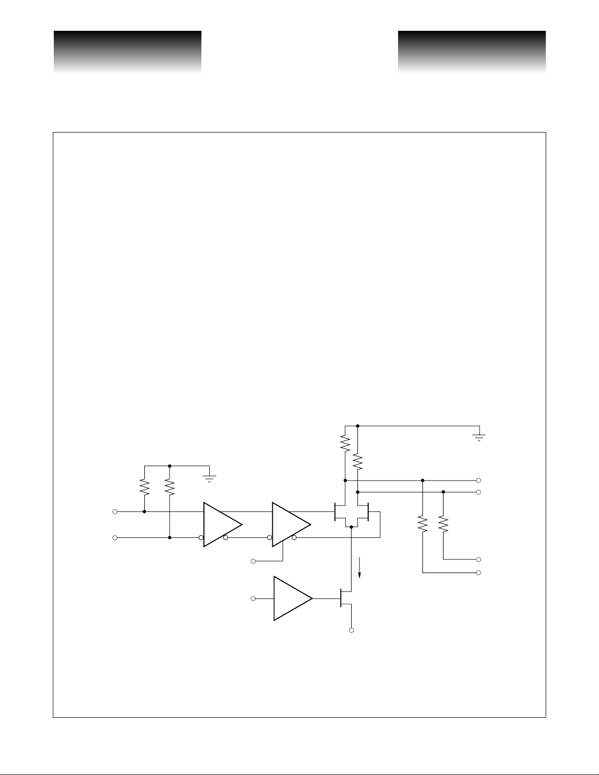
General Description
The VSC7991 is a single 7V supply, 10.7Gb/s Electroabsorption Modulator (EAM)/laser diode driver with
direct access to the laser modulation FETs. Laser offse t and modul at ion current s are set by external comp onent s
allowing precision moni t ori ng and setting of the voltage leve ls. Data inputs are differenti al ly t er min ated to 50Ω.
Applications
• SONET/SDH @ 2.488Gb/s, 9.952Gb/s, 10.7Gb/s
VSC7991 Block Diagram
(1)
50Ω
DIN
NDIN
Note: (1) On-die components.
50Ω
(1)
60Ω
(1)
60Ω
(1)
DCC
VIP
(1)
300Ω
I
MOD
IP
300Ω
NDOUT
DOUT
(1)
IB
IBN
G52321-0, Rev 2.3 Page 1
02/26/01
© VITESSE SEMICONDUCTOR CORPORATION • 741 Calle Plano • Camarillo, CA 93012
Tel: (800) VITESSE • FAX: (805) 987-5896 • Email: prodinfo@vitess e.com
Internet: www.vitesse.com
Page 2
VITESSE
SEMICONDUCTOR CORPORATION
SDH/SONET 10.7Gb/s
Advance Product Information
Electroabsorption Modulator/Laser Diode Driver
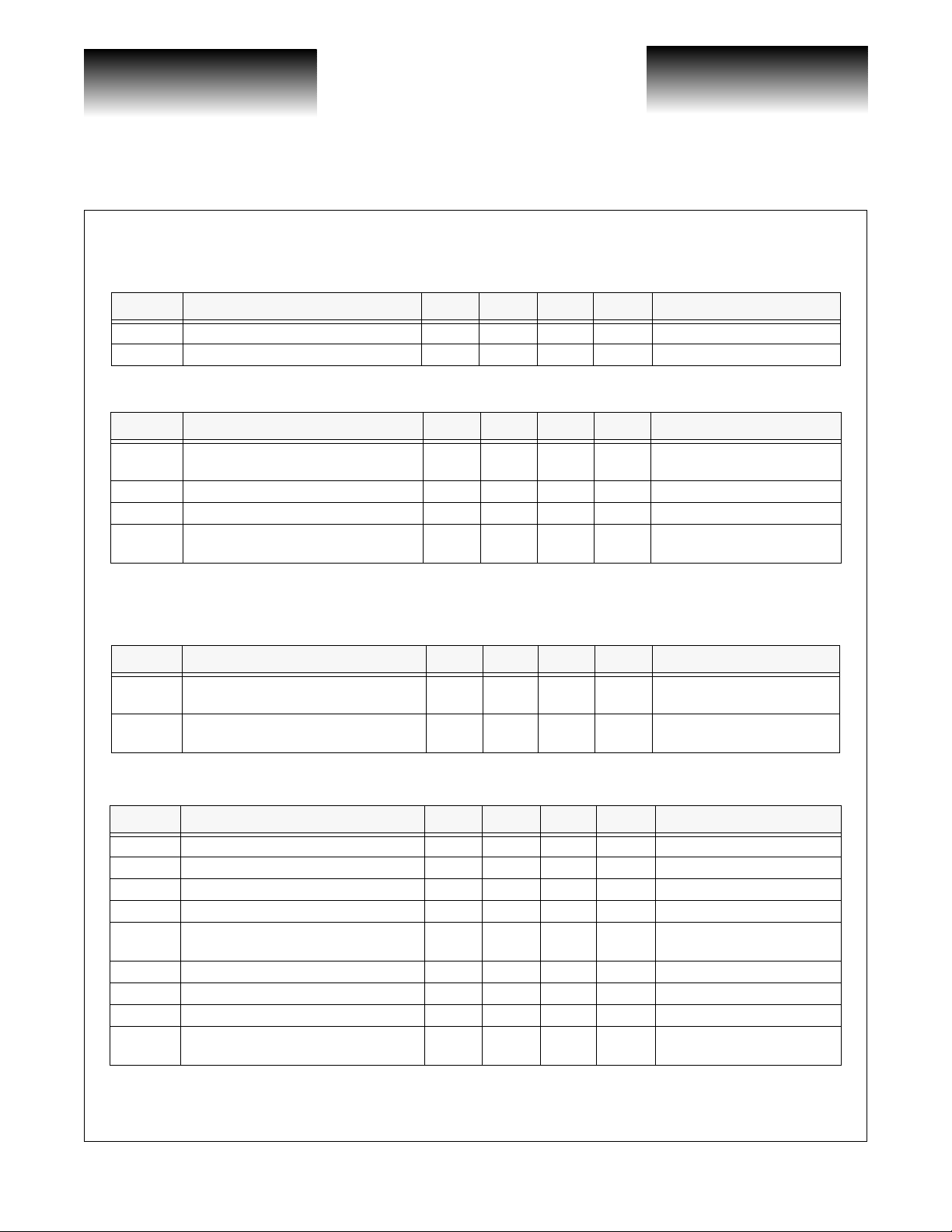
AC Characteristics (Over recommended operating conditions)
Table 1: High Speed Inputs /Outputs
Symbol Parameter Min Typ Max Units Conditions
IRL Input Return Loss, 50Ω System −15 dB 50MHz to 10GHz
ORL Output Return Loss, 50Ω System
−12 dB 50MHz to 10GHz
T able 2: Laser Driver AC Electrical Specifications
Symbol Parameter Min Typ Max Units Conditions
tR t
F
Jitter Output Jitter 15 ps/p-p 50Ω Load, V
Output Rise and Fall Times 38 ps
Overshoot/Undershoot −10 +10 %
Duty-Cycle −25 +25 %
50Ω load, 20% to 80%, V
= 3V
DCC in the range of V
0.5V to V
DC Characteristics (Over recommended operating conditions)
Table 3: Power Dissipation
VSC7991
= 3V
MOD
SS
SS
+2V
MOD
−
Symbol Parameter Min Typ Max Units Conditions
= −6.8, RL = 50Ω to GND,
V
I
P
VSS
D
Power Supply Current (V
Total Power Dissipation 2040 2244 mW
) 300 330 mA
SS
SS
I
= 120mA, V
MOD
= −6.8, RL = 50Ω to GND
V
SS
= 120mA, V
I
MOD
BIAS
BIAS
= 0V
= 0V
T able 4: Laser Driver DC Electrical Specifications
Symbol Parameter Min Typ Max Units Conditions
V
BIAS
V
MOD
V
OCM
IB, IBN L aser Bias Control Voltage −10 0V
V
IP
V
IH
V
IL
V
SW
DCC Duty-Cycle Control
NOTE: DIN and NDIN inputs need to be driven di ff erentially. If single-ended drive is desired, it is necessary to add a DC bias to the unused pin.
Programmable Output Offset Voltage −0.8 0V
Modulation Voltage Amplitude 1.5 3V
Output Voltage Compliance 4 V
Laser Modulation Control Voltage V
Input High Voltage −150 0mV
Input Low Voltage −1.00 −0.60 V
(1)
Input Voltage Swing 450 1000 mVp-p
SS
VSS −
0.5V
VSS +
0.7
VSS+
2V
V
Page 2 G52321-0, Rev 2.3
© VITESSE SEMICONDUCTOR CORPORATION • 741 Calle Plano • Camarillo, CA 93012
Tel: (800) VITESSE • FAX: (805) 987-5896 • Email: prodinfo@vitesse.com
Internet: www.vitesse.com
02/26/01
Page 3
VITESSE
SEMICONDUCTOR CORPORATION
Advance Product Information
VSC7991
Absolute Maximum Ratings
Negative Power Supply Voltage (VSS)..............................................................................................VCC to −8.0V
All Pins............................................... ........ ................................................................ .........................V
Supply Voltage (V
Supply Current (I
Input Voltage (V
Output Voltage (V
Modulation Control Voltage (V
Output Offset Control Voltage (IB, IBN)..........................................................................................................11V
Output Offset Control Current (I
Maximum Junction Temperature Range .....................................................................................−55°C to +125°C
Storage Temperature Range: .......................................................................................................−55°C to +125°C
Note:
(1) CAUTION: Stresses listed under “Absolut e Maximum Ratings” may be applied to devices one at a time without causing per-
manent damage . Fu nctionality at or above th e va lues listed is not implied . Ex p os u re to these values fo r ex te nd e d p e r iod s m ay
affect device reliability.
) ......................................................................................................................................... 8V
SS
)....................................................................................................................................500mA
SS
)........................................................................................................................................−2.0V
IN
)................................................................................................................................. −4.0V
OUT
).........................................................................................................VSS − 0.5V
IP
) .............................................................................................................. 50mA
IB
(1)
Electroabsorption Modulator/Laser Diode Driver
SONET/SDH 10.7Gb/s
SS
Recommended Operating Conditions
Positive Voltage Rail (GND).............................................................................................................................. 0V
Negative Voltage Rail (V
Operational Case Temperature (T
)...........................................................................................................−6.5V to −7.2V
SS
) ...................................................................................................0°C to 75°C
C1
to + .5V
G52321-0, Rev 2.3 Page 3
02/26/01
© VITESSE SEMICONDUCTOR CORPORATION • 741 Calle Plano • Camarillo, CA 93012
Tel: (800) VITESSE • FAX: (805) 987-5896 • Email: prodinfo@vitesse.com
Internet: www.vitesse.com
Page 4

Page 4 G52321-0, Rev 2.3
SDH/SONET 10.7Gb/s
Electroabsorption Modulator/Laser Diode Driver
Bare Die Descriptions
2354µm (0.0927")
GND
GND
VSS
VSS
VSS
GND
GND
GND
GND
IB
IB
GND
Pad 37
Pad 38
Pad 34
Pad 35
© VITESSE SEMICONDUCTOR CORPORATION • 741 Calle Plano • Camarillo, CA 93012
GND
Tel: (800) VITESSE • FAX: (805) 987-5896 • Email: prodinfo@vitesse.com
Internet: www.vitesse.com
1754µm
(0.0691")
Pad 33
DOUT
Pad 32
GND
Pad 31
GND
Pad 30
GND
Pad 29
GND
Pad 28
Pad 36
Pad 39
Pad 40
GND
Pad 41
VSC7991
Pad 42
Pad 43
Pad 44
VSS
Pad 45
Pad 46
Pad 47
GND
Pad 48
GND
Pad 1
NDIN
Pad 2
GND
Pad 3
GND
Pad 4
GND
Pad 5
GND
Pad 6
50µm
(0.002")
VITESSE
SEMICONDUCTOR CORPORATION
Figure 1: Pad Assignments
GND
Pad 11
GND
Pad 7
DIN
Pad 8
GND
Pad 9
NC
Pad 10
(0.002")
Advance Product Information
50µm
VSC7991
GND
Pad 27
NDOUT
Pad 26
GND
Pad 25
GND
IBN
IBN
Pad 24
Pad 23
NOTE: All dimensions are in micrometers. The 48 pads specified in the pad coordinates were merged into 24 larger pads.
Die Size: 2354µm x 1754µm (0.0927" x 0.0691")
Die Thickness: 381µm (0.015")
Pad Pitch: 150µm (0.0059")
Pad Size: 116µm x 116µm (0.0046" x 0.0046")
Pad Passivation Opening: 100µm x 100µm (0.0039" x 0.0039")
Scribe Size: 50µm (0.002")
IP
Pad 22IPPad 21
Pad 20
GND
Pad 19
VIP
Pad 18
VSS
Pad 17
VSS
Pad 16
VSS
Pad 15
VSS
Pad 14
DCC
Pad 13
GND
Pad 12
02/26/01
Page 5

VITESSE
SEMICONDUCTOR CORPORATION
Advance Product Information
VSC7991
Table 5: Pad Coordinates
Pad
Number
1 GND 2296 1546 25 GND 58 208
2 NDIN 2296 1396 26 NDOUT 58 358
3 GND 2296 1246 27 GND 58 508
4 GND 2296 1061.5 28 GND 58 692.5
5 GND 2296 877 29 GND 58 877
6 GND 2296 692.5 30 GND 58 1061.5
7 GND 2296 508 31 GND 58 1246
8 DIN 2296 358 32 DOUT 58 1396
9 GND 2296 208 33 GND 58 1546
10 NC 2296 58 34 IB 58 1696
11 GND 2146 58 35 IB 208 1696
12 GND 1996 58 36 GND 358 1696
13 VDCC 1846 58 37 GND 508 1696
14 VSS 1696 58 38 GND 658 1696
15 VSS 1546 58 39 GND 808 1696
16 VSS 1396 58 40 GND 958 1696
17 VSS 1246 58 41 GND 1108 1696
18 VIP 1027 58 42 VSS 1258 1696
19 GND 808 58 43 VSS 1408 1696
20 GND 658 58 44 VSS 1558 1696
21 IP 508 58 45 VSS 1708 1696
22 IP 358 58 46 GND 1858 1696
23 IBN 208 58 47 GND 2008 1696
24 IBN 58 58 48 GND 2158 1696
Signal
Name
Coordinates (µm)
X Y X Y
SONET/SDH 10.7Gb/s
Electroabsorption Modulator/Laser Diode Driver
Pad
Number
Signal
Name
Coordinates (µm)
G52321-0, Rev 2.3 Page 5
02/26/01
© VITESSE SEMICONDUCTOR CORPORATION • 741 Calle Plano • Camarillo, CA 93012
Tel: (800) VITESSE • FAX: (805) 987-5896 • Email: prodinfo@vitesse.com
Internet: www.vitesse.com
Page 6

VITESSE
SEMICONDUCTOR CORPORATION
SDH/SONET 10.7Gb/s
Electroabsorption Modulator/Laser Diode Driver
Package Pin Descriptions
Figure 2: Pin Identification
GND
GND
VSS
VSS
32
31
30
29
GND
GND
NDIN
GND
GND
DIN
GND
GND
1
2
3
4
5
6
7
8
VSC7991
T op Vie w
GND
GNDIBGND
28
27
Advance Product Information
VSC7991
26
25
24
23
22
21
20
19
18
17
GND
GND
DOUT
GND
GND
NDOUT
GND
GND
9
10
11
12
13
14
15
16
IP
VSS
VIP
VSS
DCC
GND
Page 6 G52321-0, Rev 2.3
© VITESSE SEMICONDUCTOR CORPORATION • 741 Calle Plano • Camarillo, CA 93012
Tel: (800) VITESSE • FAX: (805) 987-5896 • Email: prodinfo@vitesse.com
Internet: www.vitesse.com
IBN
GND
02/26/01
Page 7

VITESSE
SEMICONDUCTOR CORPORATION
Advance Product Information
VSC7991
Table 6: Pin Identifications
Pin # Name Type Level Description
1 GND Pwr Pwr Positive Voltage Rail
2 GND Pwr Pwr Positive Voltage Rail
3 NDIN In CML Complementary Data In
4 GND Pwr Pwr Positive Voltage Rail
5 GND Pwr Pwr Positive Voltage Rail
6 DIN In CML Data In
7 GND Pwr Pwr Positive Voltage Rail
8 GND Pwr Pwr Positive Voltage Rail
9 GND Pwr Pwr Positive Voltage Rail
10 DCC In DC Duty-Cycle Control Voltage
11 VSS Pwr Pwr Negative Voltage Rail
12 VSS Pwr Pwr Negative Voltage Rail
13 VIP In DC Modulation Control Voltage
14 IP In DC Modulation Current Monitor
15 IBN In DC Data Offset Control Current (complementary)
16 GND Pwr Pwr Positive Voltage Rail
17 GND Pwr Pwr Positive Voltage Rail
18 GND Pwr Pwr Positive Voltage Rail
19 NDOUT Out Laser Modulation Current Output (complemen ta ry)
20 GND Pwr Pwr Positive Voltage Rail
21 GND Pwr Pwr Positive Voltage Rail
22 DOUT Out Laser Modu la tion Current Output
23 GND Pwr Pwr Positive Voltage Rail
24 GND Pwr Pwr Positive Voltage Rail
25 GND Pwr Pwr Positive Voltage Rail
26 IB In DC Data Offset Control Current
27 GND Pwr Pwr Positive Voltage Rail
28 GND Pwr Pwr Positive Voltage Rail
29 VSS Pwr Pwr Negative Voltage Rail
30 VSS Pwr Pwr Negative Voltage Rail
31 GND Pwr Pwr Positive Voltage Rail
32 GND Pwr Pwr Positive Voltage Rail
SONET/SDH 10.7Gb/s
Electroabsorption Modulator/Laser Diode Driver
NOTE: A voltage HIGH on the data input (pin 6) corresponds to a voltage HIGH on the data output (pin 22).
G52321-0, Rev 2.3 Page 7
02/26/01
© VITESSE SEMICONDUCTOR CORPORATION • 741 Calle Plano • Camarillo, CA 93012
Tel: (800) VITESSE • FAX: (805) 987-5896 • Email: prodinfo@vitesse.com
Internet: www.vitesse.com
Page 8

VITESSE
SEMICONDUCTOR CORPORATION
SDH/SONET 10.7Gb/s
Electroabsorption Modulator/Laser Diode Driver
Package Information
Advance Product Information
VSC7991
DIMS TOL. DIM
A REF 0.054
A1 ±0.003 0.003
A2 REF 0.050
D ±0.010 0.321
D1 ±0.005 0.225
E ±0.010 0.321
E1 ±0.005 0.225
L ±0.005 0.021
e REF 0.0256
b TYP 0.011
ddd N/A 0.004
θ
N/A 0° - 10°
CCC MAX 0.004
R1 ±0.003 0.005
R ±0.003 0.005
Shoulder
-
0.020
θ
All dimens ions in inches.
Page 8 G52321-0, Rev 2.3
© VITESSE SEMICONDUCTOR CORPORATION • 741 Calle Plano • Camarillo, CA 93012
Tel: (800) VITESSE • FAX: (805) 987-5896 • Email: prodinfo@vitesse.com
Internet: www.vitesse.com
02/26/01
Page 9

VITESSE
SEMICONDUCTOR CORPORATION
Advance Product Information
VSC7991
Ordering Informatio n
The order number for this product is formed by a combination of the device number, and package style.
Device Type
VSC7991:
SONET/SDH 10.7Gb/s Laser Diode Driver
VSC7991
SONET/SDH 10.7Gb/s
Electroabsorption Modulator/Laser Diode Driver
xx
Package Style
CD: Metal Glass with Metal Lid—Formed Leads
X : Bare Die
Notice
Vitesse Semiconductor Corporation (“Vitesse”) provides this document for informational purposes only. This document contains pre-production
information about Vitesse products in their conce pt, development and/or testi ng phase. All informaiton in this document, including de scriptions of
features, f u nctions, performance, technical specifications and av ailability , is subject to ch ange without notice at any time. Nothing contained in this
document shall be con stru ed a s e xtend ing any w arr anty or prom ise, exp ress or im plied , th at a ny Vitesse produ ct wi ll b e av ail able as described or
will be suitable for or will accompli sh any particular task.
Vitesse products are not intended for use in life support appliances, devices or systems. Use of a Vitesse product in such applications without written consent is prohibited.
G52321-0, Rev 2.3 Page 9
02/26/01
© VITESSE SEMICONDUCTOR CORPORATION • 741 Calle Plano • Camarillo, CA 93012
Tel: (800) VITESSE • FAX: (805) 987-5896 • Email: prodinfo@vitesse.com
Internet: www.vitesse.com
Page 10

VITESSE
SEMICONDUCTOR CORPORATION
SDH/SONET 10.7Gb/s
Electroabsorption Modulator/Laser Diode Driver
This page left intentionally blank.
Advance Product Information
VSC7991
Page 10 G52321-0, Rev 2.3
© VITESSE SEMICONDUCTOR CORPORATION • 741 Calle Plano • Camarillo, CA 93012
Tel: (800) VITESSE • FAX: (805) 987-5896 • Email: prodinfo@vitesse.com
Internet: www.vitesse.com
02/26/01
 Loading...