

Page 1

VITESSE
SEMICONDUCTOR CORPORATION
Advance Product Information
VSC7990
SONET/SDH 10.7Gb/s
Laser Diode Driver
G52303-0, Rev 2.2 Page 1
04/05/01
© VITESSE SEMICONDUCTOR CORPORATION • 741 Calle Plano • Camarillo, CA 93012
Tel: (800) VITESSE • FAX: (805) 987-5896 • Email: prodinfo@vitesse.com
Internet: www.vitesse.com
Features
General Description
The VSC7990 is a single +5V or −5.2V supply, 10.7Gb/s laser diode driver with direct access to the laser
modulation and bias FETs. Laser bias and modulation currents are set by external components allowing precision monitoring and setting of the current levels. Clock and data inputs are differentially terminated to 50
Ω and
must be AC-coupled. The superl at ive edge- rat e and dr iv e cur re nt of t he VSC7990 enables efficient design of an
OC-192/STM-64 transmitter using di rect ly modul at ed lase r diod es. A two- chi p OC-12 to OC-1 92 opti cal transmitter can be easily implemented using the VSC7990 and the VSC8171 10Gb/s MUX/CRU.
Applications
• OC-192/STM-64 @ 2.488Gb/s to 10.7Gb/s
• 10Gb/s Serial Ethernet
VSC7990 Block Diagram
• 100mA Available Modulation Current
• 100mA Available Bias Current
• 10.7Gb/s Operation
• Duty Cycle Control
• Single Power Supply
• Direct Access to Modulation and Bias FETs
• On-chip Reclocking Register
• On-chip MUX for Selectable Clocked or Unclocked
Applications
• On-chip 50
Ω Input Termination for Clock and Data
• Av ailab le in Tested Bare Die
50Ω
(2)
D
MUX
Q
DIN
PWN
PWP
VTHD
(1)
50Ω
(2)
NDIN
VTHDN
(1)
50Ω
(2)
(2)
CLK
NCLK
I
MOD
VIB
3Ω
VIP
CLKSEL
MIP
I
BIAS
MIB
IOUT
NIOUT
IBIAS
NOTES: (1) Terminated to off-chip capacitor. (2) On-die components.
3Ω
50Ω
(2)
(2)
Page 2
VITESSE
SEMICONDUCTOR CORPORATION
Advance Product Inf ormation
VSC7990
SONET/SDH 10.7Gb/s
Laser Diode Driver
Page 2 G52303-0, Rev 2.2
04/05/01
© VITESSE SEMICONDUCTOR CORPORATION • 741 Calle Plano • Camarillo, CA 93012
Tel: (800) VITESSE • FAX: (805) 987-5896 • Email: prodinfo@vitesse.com
Internet: www.vitesse.com
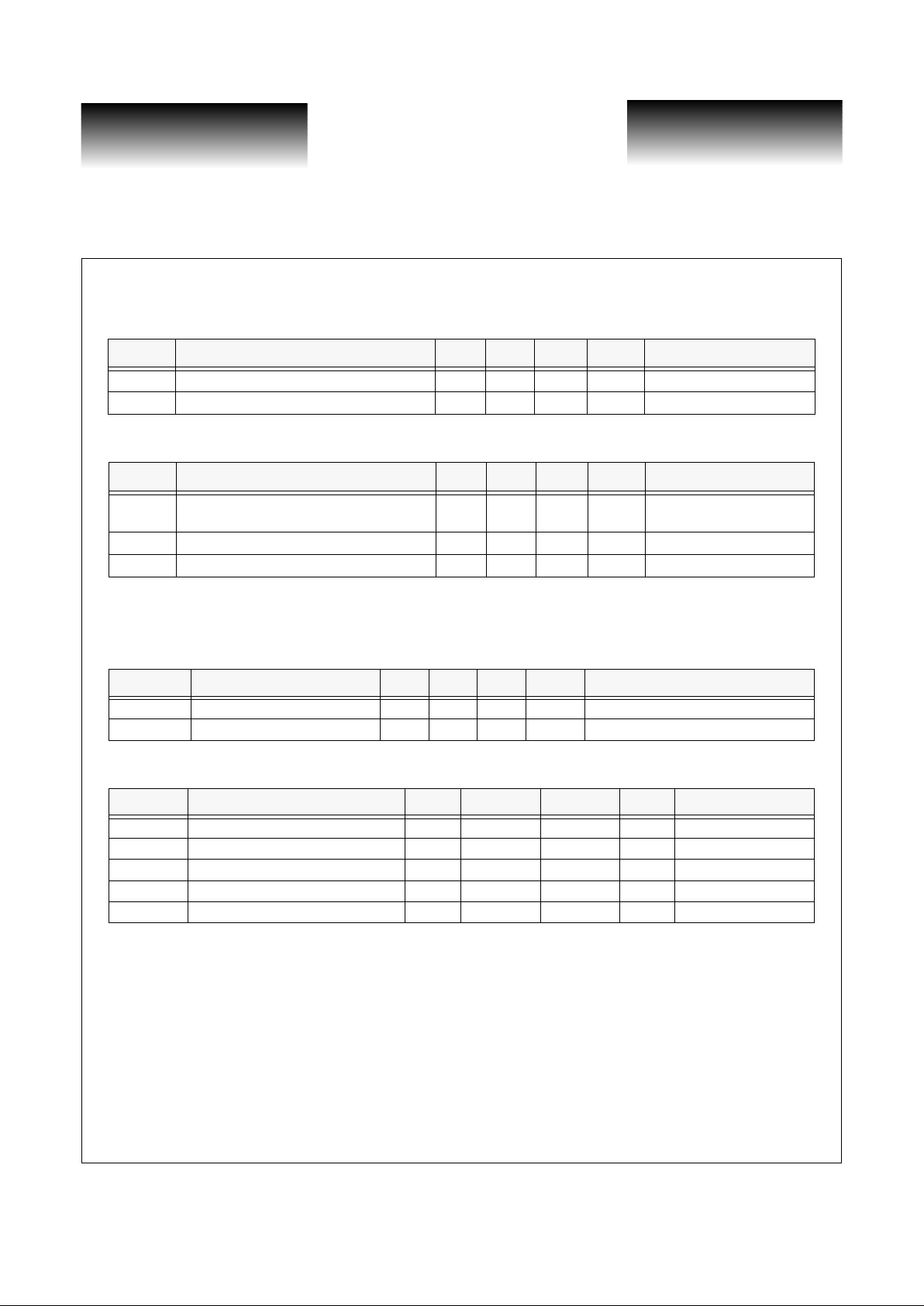
AC Characteristics (Over recommended operating conditions)
Table 1: High-Speed Inputs and ECL Outputs
Table 2: Laser Driver AC Electrical Specifications
DC Characteristics (Over recommended operating conditions)
Table 3: Power Dissipat ion
Table 4: Laser Driver DC Electrical Specifications
Symbol Parameter Min Typ Max Units Conditions
V
IN
Single-ended Input Voltage Swing 400 1000 mVp-p V
CM
= −3.7V
V
IN
On-Chip Terminations 35 65 Ω
Symbol Parameter Min Typ Max Units Conditions
tR, t
F
Output Rise and Fall Times 35 ps
RL = 25Ω, 20% to 80%,
20mA < I
MOD
< 100mA
t
SU
Data to Clock Setup Time TBD ps
t
H
Hold Time TBD ps
Symbol Parameter Min Typ Max Units Conditions
I
VSS
Power Supply Current (VSS) 150 mA VSS = −5.5V, I
MOD
= I
BIAS
= 0mA
P
D
Total Power Dissipation 800 mW VSS = −5.5V, I
MOD
= I
BIAS
= 0mA
Symbol Parameter Min Typ Max Units Conditions
I
BIAS
Programmable Laser Bias Current 2 100 mA
I
MOD
Programmabl e Mo du la tio n Cur re nt 1 100 mA
V
IB
Laser Bias Contr ol Voltage VSS+2.1V V I
BIAS
= 60mA
V
IP
Laser Modulation Control Voltage VSS+2.1V V I
MOD
= 100mA
V
OCM
Output Voltage Compliance GND −3V VV
SS
= −5.2V
Page 3

VITESSE
SEMICONDUCTOR CORPORATION
Advance Product Information
VSC7990
SONET/SDH 10.7Gb/s
Laser Diode Driver
G52303-0, Rev 2.2 Page 3
04/05/01
© VITESSE SEMICONDUCTOR CORPORATION • 741 Calle Plano • Camarillo, CA 93012
Tel: (800) VITESSE • FAX: (805) 987-5896 • Email: prodinfo@vitesse.com
Internet: www.vitesse.com
Table 5: MUX Select Logic Table
Table 6: MOD_EN Logic Table
Absolute Maximum Ratings
(1)
Negative Power Supply Voltage (VSS)...........................................................................................................-6.0V
All Pins............................................... ........ .......................................................................................V
SS
to + 0.5V
Supply Voltage (V
SS
) .....................................................................................................................................-6.0V
Supply Current (I
SS
)....................................................................................................................................300mA
Input Voltage (V
IN
).............................................................................................................................VSS to +0.5V
Modulation Control Voltage (V
IP
)......................................................................................................VSS to +0.5V
Maximum Junction Temperature Range ......................................................................................-55°C to +125°C
Storage Temperature Range .........................................................................................................-65°C to +150°C
NOTE: (1) CAUTION: Stresses listed under “Absolute Maximum Ratings” may be applied to devices one at a time without caus-
ing permanent damage. Functionality at or above the values listed is not implied. Exposure to these values for extended
periods may affect device reliability.
Recommended Operating Conditions
Positive Voltage Rail (GND, VDD)..................................................................................................................... 0V
Negative Voltage Rail (V
SS
).............................................................................................................-5.5V to -4.9V
Junction Temperature Operating Range (T
J
) ...................................................................................0°C to +125°C
SEL
Mode Select
V
SS
Clocked Data In
GND (V
DD
) Unclocked Data In
N/C Unclocked Data In
SEL
Mode Select
V
SS
Modulation Current Enabled
GND (V
DD
) Modulation Current Disabled
Page 4

VITESSE
SEMICONDUCTOR CORPORATION
Advance Product Inf ormation
VSC7990
SONET/SDH 10.7Gb/s
Laser Diode Driver
Page 4 G52303-0, Rev 2.2
04/05/01
© VITESSE SEMICONDUCTOR CORPORATION • 741 Calle Plano • Camarillo, CA 93012
Tel: (800) VITESSE • FAX: (805) 987-5896 • Email: prodinfo@vitesse.com
Internet: www.vitesse.com
Figure 1: Single-Ended AC-Coupled
Data
Source
0.1µF
0.1µF
DIN
50Ω
(1)
50Ω
(1)
7kΩ
(1)
2.6kΩ
(1)
V
SS
VTHD
(1) On-chip components.
V
SS
7kΩ
(1)
2.6kΩ
(1)
V
SS
0.1µF
NDIN
0.1µF
VTHDN
Clock
Source
0.1µF
CLK
50Ω
(1)
50Ω
(1)
7kΩ
(1)
2.6kΩ
(1)
(1)
(1)
V
SS
V
SS
7kΩ
(1)
2.6kΩ
(1)
V
SS
0.1µF
Chip
Boundary
NCLK
Page 5

VITESSE
SEMICONDUCTOR CORPORATION
Advance Product Information
VSC7990
SONET/SDH 10.7Gb/s
Laser Diode Driver
G52303-0, Rev 2.2 Page 5
04/05/01
© VITESSE SEMICONDUCTOR CORPORATION • 741 Calle Plano • Camarillo, CA 93012
Tel: (800) VITESSE • FAX: (805) 987-5896 • Email: prodinfo@vitesse.com
Internet: www.vitesse.com
Figure 2: Differential AC-Coupled
Data
Source
0.1µF
0.1µF
0.1µF
0.1µF
DIN
50Ω
(1)
50Ω
(1)
7kΩ
(1)
2.6kΩ
(1)
V
SS
VTHD
(1) On-chip components.
V
SS
7kΩ
(1)
2.6kΩ
(1)
V
SS
NDIN
0.1µF
VTHDN
Clock
Source
0.1µF
CLK
50Ω
(1)
50Ω
(1)
7kΩ
(1)
2.6kΩ
(1)
(1)
(1)
V
SS
V
SS
7kΩ
(1)
2.6kΩ
(1)
V
SS
Chip
Boundary
NCLK
Page 6

VITESSE
SEMICONDUCTOR CORPORATION
Advance Product Inf ormation
VSC7990
SONET/SDH 10.7Gb/s
Laser Diode Driver
Page 6 G52303-0, Rev 2.2
04/05/01
© VITESSE SEMICONDUCTOR CORPORATION • 741 Calle Plano • Camarillo, CA 93012
Tel: (800) VITESSE • FAX: (805) 987-5896 • Email: prodinfo@vitesse.com
Internet: www.vitesse.com
Figure 3: Control Signals VIP and VIB
Figure 4: Simplified Output Structure
30mA
60mA
I (MIB)
I (MIP)
VIP
VIB
V
SS
+ 1.5V (typical)
V
SS
+ 1.5V (typical)
Typical Bias Current vs. Bias Voltage
Typical Modulation Current vs. Modulation Voltage
I
MOD
v
SS
VIP
MIP
VIB
MIB
I
BIAS
I
BIAS
V
DD
Output
Differential
Pair
NIOUT IOUT
2.5kΩ 2.5kΩ3Ω 3Ω
500Ω
300Ω
v
SS
Page 7

VITESSE
SEMICONDUCTOR CORPORATION
Advance Product Information
VSC7990
SONET/SDH 10.7Gb/s
Laser Diode Driver
G52303-0, Rev 2.2 Page 7
04/05/01
© VITESSE SEMICONDUCTOR CORPORATION • 741 Calle Plano • Camarillo, CA 93012
Tel: (800) VITESSE • FAX: (805) 987-5896 • Email: prodinfo@vitesse.com
Internet: www.vitesse.com
Package Pin Descriptions
Figure 5: Pad Assignments
2159µm (0.085")
1270
µm
(0.050")
VSC7990
0.002"
(51µm)
0.002"
(51µm)
Die Size with Scribe: 2159µm x 1270µm (0.085" x 0.050")
Die Thickness: 381µm (0.015")
Pad Pitch: 127µm (0.005")
Pad to Pad Clearance: 51µm (0.002")
Pad Size: 77µm x 77µm (0.003" x 0.003")
Pad Passivation Opening: 76.2µm x 76.2µm (0.003" x 0.003")
Scribe Size: 50µm (0.002")
Pad 39
IBIAS
Pad 40
IBIAS
Pad 38
VDD
Pad 37
VDD
Pad 36
VDD
Pad 35
VDD
Pad 34NCPad 33
VDD
Pad 32
IOUT
Pad 31
VDD
Pad 30
NIOUT
Pad 29
VDD
Pad 28NCPad 27
VDD
Pad 26
VDD
Pad 25
VDD
Pad 24
VDD
Pad 23
VIP
Pad 22
MIP
Pad 21
VSS
Pad 20
VSS
Pad 19
MOD_EN
Pad 18
PWN
Pad 17
PWP
Pad 2
VDD
Pad 3
DIN
Pad 4
VDD
Pad 5
NDIN
Pad 6
VDD
Pad 7
CLK
Pad 8
VDD
Pad 9
CLKN
Pad 10
VDD
Pad 11
VDD
Pad 12
VDD
Pad 13
VDD
Pad 14
CLKSEL
Pad 15
VDD
Pad 16
NC
Pad 41
NC
Pad 42
VIB
Pad 43
MIB
Pad 44
VSS
Pad 45
VSS
Pad 46
VTHDN
Pad 1
VTHD
Page 8

VITESSE
SEMICONDUCTOR CORPORATION
Advance Product Inf ormation
VSC7990
SONET/SDH 10.7Gb/s
Laser Diode Driver
Page 8 G52303-0, Rev 2.2
04/05/01
© VITESSE SEMICONDUCTOR CORPORATION • 741 Calle Plano • Camarillo, CA 93012
Tel: (800) VITESSE • FAX: (805) 987-5896 • Email: prodinfo@vitesse.com
Internet: www.vitesse.com
Table 7: Pad Locations for VSC7990 Die
Pin # Signal Name Signal Type Levels Description
1VTHD——Input Bias Thresh old Ad jus t, True
2VDD— 0V Ground
3DIN IECL
(1)
Data Input, True
4VDD— 0V Ground
5 NDIN I ECL
(1)
Data Input, Complement
6VDD— 0V Ground
7CLK IECL
(1)
Clock Input, True
8VDD— 0V Ground
9CLKN IECL
(1)
Clock Input, Comp le m en t
10 VDD — 0V Ground
11 VDD — 0V Ground
12 VDD — 0V Ground
13 VDD — 0V Ground
14 CLKSEL I — Clock Select (see Table 5)
15 VDD — 0V Ground
16 NC ——No Connection
17 PWP I — Duty Cycle Control, Positive
18 PWN I — Duty Cycle Control, Negative
19 MOD_EN I ECL Modulation Output Enable
20 VSS —–5.2V Power Supply
21 VSS —–5.2V Power Supply
22 MIP O — Modulation Current Monitor
23 VIP I — Modulation Set Voltage
24 VDD — 0V Ground
25 VDD — 0V Ground
26 VDD — 0V Ground
27 VDD — 0V Ground
28 NC ——No Connection
29 VDD — 0V Ground
30 NIOUT O — Modulation Current Out, Complement
31 VDD — 0V Ground
32 IOUT O — Modulation Curre nt Out, True
33 VDD — 0V Ground
34 NC ——No Connection
35 VDD — 0V Ground
36 VDD — 0V Ground
37 VDD — 0V Ground
Page 9

VITESSE
SEMICONDUCTOR CORPORATION
Advance Product Information
VSC7990
SONET/SDH 10.7Gb/s
Laser Diode Driver
G52303-0, Rev 2.2 Page 9
04/05/01
© VITESSE SEMICONDUCTOR CORPORATION • 741 Calle Plano • Camarillo, CA 93012
Tel: (800) VITESSE • FAX: (805) 987-5896 • Email: prodinfo@vitesse.com
Internet: www.vitesse.com
NOTE: (1) Data and clock input s are ECL-sw ing but not ECL level. Inputs must be AC-coupled as shown in Figures 2 and 3 of
this data sheet.
38 VDD — 0V Ground
39 IBIAS O — Bias Current Output
40 IBIAS O — Bias Current Output
41 NC ——No Connection
42 VIB I — Bias Output Adjust
43 MIB O — Bias Current Monitor
44 VSS —–5.2V Power Supply
45 VSS —–5.2V Power Supply
46 VTHDN ——Input Bias Threshold Adjust for Data, Complement
Pin # Signal Name Signal Type Levels Description
Page 10

VITESSE
SEMICONDUCTOR CORPORATION
Advance Product Inf ormation
VSC7990
SONET/SDH 10.7Gb/s
Laser Diode Driver
Page 10 G52303-0, Rev 2.2
04/05/01
© VITESSE SEMICONDUCTOR CORPORATION • 741 Calle Plano • Camarillo, CA 93012
Tel: (800) VITESSE • FAX: (805) 987-5896 • Email: prodinfo@vitesse.com
Internet: www.vitesse.com
Ordering Informatio n
The order number for this product is formed by a combination of the device type and package style.
VSC7990
XX
Device Type
SONET/SDH 10.7Gb/s Laser Diode Driver
Package Style
W : Bare die in waffle pack
Notice
Vitesse Semiconductor Corporation (“Vitesse”) provides this document for informational purposes only. This document contains pre-production
information about Vitesse products in their conce pt, development and/or testi ng phase. All information in t his document, including de scriptions of
features, functions, performa n ce, technical specif ications and availability, is subject to change without notice at any time. Nothing contained in this
document shall be con stru ed a s e xten ding an y warr an ty or pr omise , ex press or imp lied, that any Vitesse product wil l be avai lab le as described or
will be suitable for or will accompli sh any particular task.
Vitesse products are not intended for use in life support applia nc es, devices or systems. Use of a Vitesse product in such applications without written consent is prohibited
 Loading...