

Page 1

VITESSE
SEMICONDUCTOR CORPORATION
Advance Product Information
VSC7962
3.125Gb/s PECL Limiting Amplifi er with LOS Detect
and Laser Driver with Automatic Powe r Control
G52361-0, Rev 2.1 Page 1
05/01/01
© VITESSE SEMICONDUCTOR CORPORATION • 741 Calle Plano • Camarillo, CA 93012
Tel: (800) VITESSE • FAX: (805) 987-5896 • Email: prodinfo@vitesse.com
Internet: www.vitesse.com
Features Applications
General Description
The VSC7962 is a single 3.3V supply combination limiting amplifier and laser diode driver for
SONET/SDH applications up to 3.125Gb/s. The limiting amplifier features Loss of Signal (LOS) detect, output
offset correction, and optional output squelch. Laser driver data inputs accept differential PECL signals and the
output modulation and bias currents are easily controlled via external components. The laser diode driver Automatic Power Control (APC) loop mai ntains a con sta nt average o ptical power o ver te mperature and l ife time. The
dominant pole of the APC loop can be controlled with an external capacitor. Other features include enable control, short-circuit protection for the modulation a nd bias inputs, short rise and fall times, and failure-mo nitor
output to indicate when the APC loop is unable to maintain the average optical power. The VSC7962 is available in die form or in a 48-pin TQFP package. The VSC7960 provides similar features to the VSC7962 but the
limiting amplifier has CML outputs.
Block Diagram
• 3.3V Power Supply
• Laser Driver AC-Coupled to Laser Diode
• Programmable Laser Driver Modulation Current
from 5mA to 60mA
• Programmable Laser Driver Bias Current from
1mA to 100mA
• Laser Driver Enable Control
• Automatic Optical Average Power Control
• Supply Current of 80mA
• PECL Limiting Amplifier Outputs
• 48-Pin TQFP Package
• SONET/SDH at 622Mb/s, 1.244Gb/s, 2.488Gb/s
and 3.125Gb/s
• Full-Speed Fibre Channel (1.062Gb/s)
VSC7939
VSC7961
Limiting Amplifier
Laser Driver
DA TA+
DA TA-
LAO+
LAO-
OUT+
OUT -
IN+ IN-
VSC7962
Page 2
VITESSE
SEMICONDUCTOR CORPORATION
Advance Product Information
VSC7962
3.125Gb/s PECL Limiting Amplifier with LOS Detect
and Laser Driver with Automatic Power Control
Page 2 G52361-0, Rev 2.1
05/01/01
© VITESSE SEMICONDUCTOR CORPORATION • 741 Calle Plano • Camarillo, CA 93012
Tel: (800) VITESSE • FAX: (805) 987-5896 • Email: prodinfo@vitesse.com
Internet: www.vitesse.com
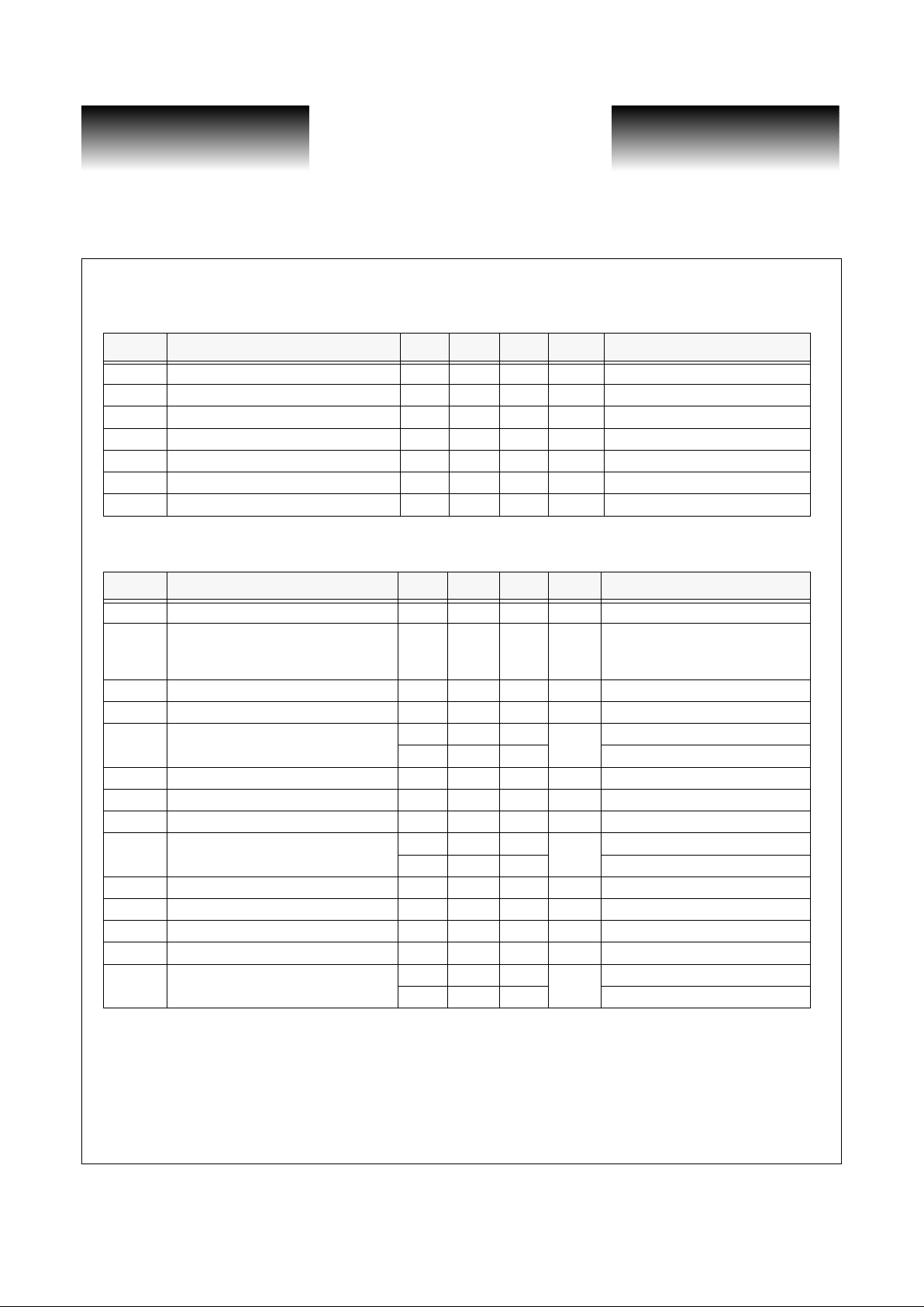
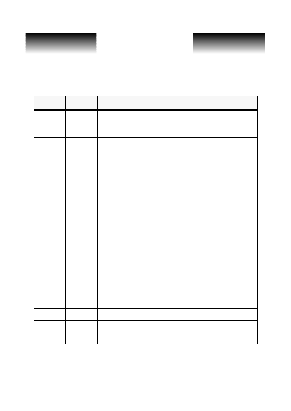
Electrical Characteristics
Table 1: Limiting Amplifier DC Specifications
NOTE: (1) See Figure5 for supply current measurement setup.
Table 2: Laser Driver DC Specifications
NOTES: (1) Both I
BIAS
and I
MOD
will turn off if any of the current set pins are grounded. (2) Assumes laser diode to monitor diode transfer
function does not change with temperature.
Symbol Parameter Min Typ Max Units Conditions
V
CC
Power Supply Range 3.135 5.5 V
I
CC
Power Supply Current
(1)
31 mA VCC = 3.3V
I
EE
Power Supply Current
(1)
38 mA VCC = 3.3V
I
CCSQ
Power Supply Current when Squelched
(1)
21 mA VCC = 3.3V
I
EESQ
Power Supply Current when Squelched
(1)
24 mA VCC = 3.3V
I
SQ
Squelch Input Curr en t 0 400 µA
PSSR Power Sup ply Rejection Ratio 20 30 dB f < 2MHz
Symbol Parameter Min Typ Max Units Conditions
V
CC
Power Supply Voltage Ran ge 3.125 3.465 V
I
CC
Supply Current TBD 45 mA
R
MODSET
=7.3kΩ,
R
BIASMAX
=4.8kΩ
I
BIAS
and I
MOD
excluded VCC=5V
I
BIAS
Bias Current Range 1 100 mA Voltage at BIAS pin=(VCC-1.6)
I
BIAS-OFF
Bias Off Current 100 µA ENABLE=low or DISABLE=high
(1)
S
BIAS
Bias Current Stability
230
ppm/°C
APC open loop. I
BIAS
=100mA
900 APC open loop. I
BIAS
=1mA
Bias Current Absolute Accuracy ±15 % Refers to part-to-part variation.
VR
MD
Monitor Diode Reve r se B ia s Vo lta g e 1.5 V
I
MD
Monitor Diode Reverse Current Range 18 1000 µA
Monitor Diode Bias Setpoint Stability
-480 50 480
ppm/°C
I
MD
=1mA
(1)
90 IMD=18µA
(1)
Monitor Diode Bias Absolute Accuracy -15 15 % Refers to part-to-part variation.
I
MOD
Modulation Current Range 5 60 mA
I
MOD-OFF
Modulation Off Current 200 µA ENABLE=low or DISABLE=high
(2)
Modulation Current Absolute Accuracy ±15 % See Note 2
Modulation Current Stability
-480 -50 480
ppm/°C
I
MOD
=60mA
250 I
MOD
=5mA
Page 3
VITESSE
SEMICONDUCTOR CORPORATION
Advance Product Information
VSC7962
3.125Gb/s PECL Limiting Amplifi er with LOS Detect
and Laser Driver with Automatic Powe r Control
G52361-0, Rev 2.1 Page 3
05/01/01
© VITESSE SEMICONDUCTOR CORPORATION • 741 Calle Plano • Camarillo, CA 93012
Tel: (800) VITESSE • FAX: (805) 987-5896 • Email: prodinfo@vitesse.com
Internet: www.vitesse.com
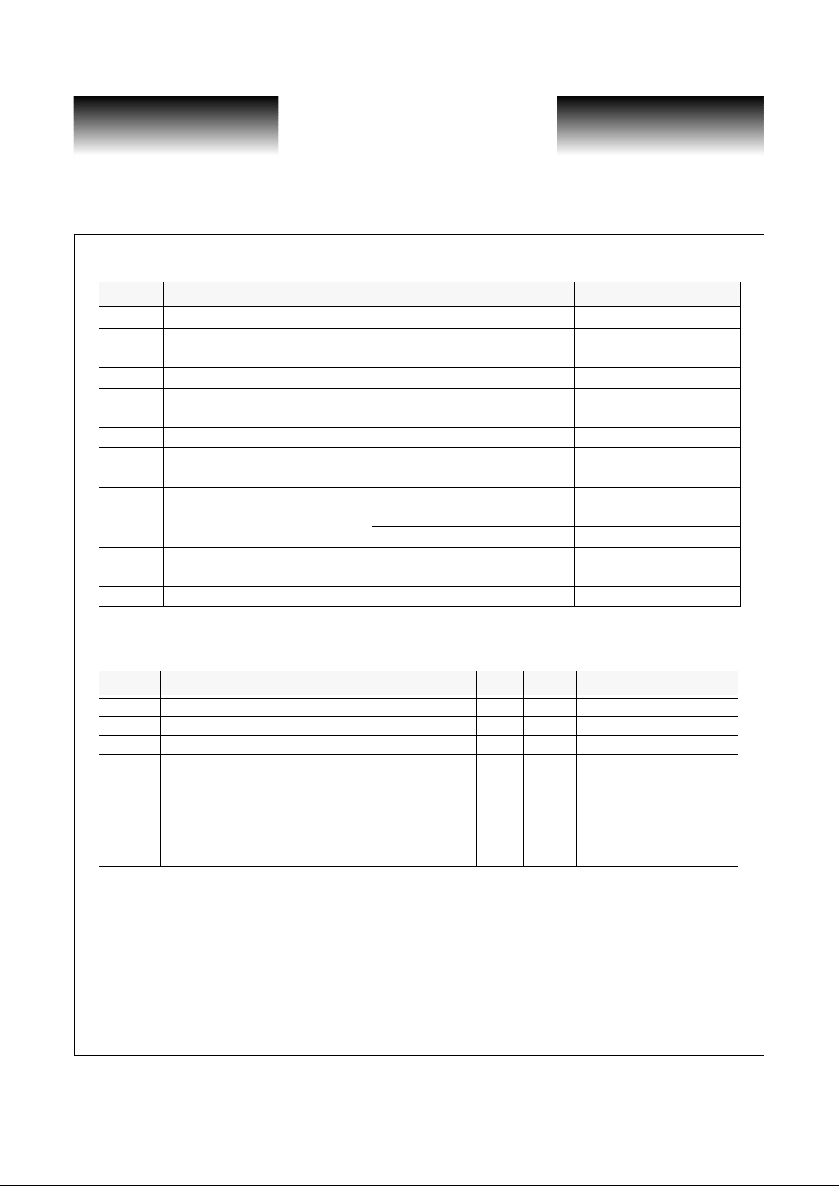
Table 3: Limiting Amplifier AC Specifications
NOTES: (1) Deterministic Jitter measured peak-to-peak with K28.5 pattern. (2) Random Jitter measured with minimum input.
Table 4: Laser Driver AC Specifications
NOTES: (1) Measured with 622Mb /s 0- 1 pattern, LATCH=high. (2) PW D = (wider pulse - na rrower pul s e) / 2)
Symbol Parameter Min Typ Max Units Conditions
Data Rate 3.125 Gb/s
V
IN
Input Voltage Range 10 1200 mV peak-to-peak
J
D
Deterministic Jitter 25 ps See Note 1
J
R
Random Jitter 8 ps rms, see Note 2
t
R, tF
Rise/Fall Times 55 100 ps 20%-80%
v
N
Input Referred Noise 230 µV rms, IN+ to IN-
R
DIFF
Differential Input Resistance 100 W IN+ to IN-
f
L
Low Frequency Cut-of f
2MHzC
Z
open
2kHzC
Z
=0.1µF
V
SQ
Output Signal when Sq ue lc he d 20 mV Outputs AC-coupled
V
OH
PECL Output High Voltage
-1025 -850 mV
-850 mV Squelched
V
OL
PECL Output Low Voltage
-1810 -1620 mV
-1620 mV Squelched
Z
O
Output Resistance 100 Ω Single-ended
Symbol Parameter Min Typ Max Units Conditions
t
SU
Input Latch Setup Time 100 ps LATCH=high
t
H
Input Latch Hold Time 100 ps LATCH=high
Enable/Start-up Delay 250 ns
t
R
Output Rise Time 60 80 ps 20% to 80%
t
F
Output Fall Time 60 80 ps 20% to 80%
PWD Pulse Width Distortion 10 50 ps See Notes 1, 2
CID
MAX
Maximum Consecutive Identical Digits 80 bits
t
J
Jitter Generation 7 20 ps
p-p
Jitter BW=12kHz to 20MHz,
0-1 pattern.
Page 4
VITESSE
SEMICONDUCTOR CORPORATION
Advance Product Information
VSC7962
3.125Gb/s PECL Limiting Amplifier with LOS Detect
and Laser Driver with Automatic Power Control
Page 4 G52361-0, Rev 2.1
05/01/01
© VITESSE SEMICONDUCTOR CORPORATION • 741 Calle Plano • Camarillo, CA 93012
Tel: (800) VITESSE • FAX: (805) 987-5896 • Email: prodinfo@vitesse.com
Internet: www.vitesse.com
Table 5: PECL and TTL/CMOS Inputs and Outputs Specifications
Table 6: Limiting Amplifier Loss of Signal Specifications
Table 7: Limiting Amplifier Loss of Signal Truth Table
Symbol Parameter Min Typ Max Units Conditions
V
ID
Differential Input Voltage 100 1600 mV
p-p
(DATA+) - (DATA-)
V
ICM
Common-Mode Input Voltage
V
CC
-
1.49
VCC -
1.32
VCC V
ID
/4
V PECL compatible
I
IN
Clock and Data Input Current -1 10 µA
V
IH
TTL Input High Voltage
(ENABLE, LATCH, DISABLE)
2.0 V
V
IL
TTL Input Low Voltage
(ENABLE, LATCH, DISABLE)
0.8 V
V
OH
TTL Output High Voltage (FAIL)2.4
V
CC
-
0.3
V
CC
V Sourcing 50µA
V
OL
TTL Output Low Voltage (FAIL) 0.1 0.44 V Sinking 100µA
Symbol Parameter Min Typ Max Units Conditions
H
LOS
LOS Hysteresis 3.1 3.3 5.5 dB H
LOS
= 20 log (V
THD
/ V
THA
)
t
LOS
LOS Assert / Deassert Time 0.22 0.25 0.28 µs
V
THA
LOS Assert Threshold
8.2
mV
R
TH
=2.5kΩ
12.8 19.8 21.8 R
TH
=7kΩ
57.2 RTH=20kΩ
V
THD
LOS Deassert Threshold
11.4
mV
R
TH
=2.5kΩ
26.2 29 31.6 R
TH
=7kΩ
75.2 RTH=20kΩ
V
LOSH
LOS Output High Voltage 3.3 V I
LOS
=-30µA
V
LOSL
LOS Output Low Voltage 0.168 V I
LOS
=+1.2µA
SQUELCH LOS Output
High High Off
Low High On
High Low On
Low Low On
Page 5
VITESSE
SEMICONDUCTOR CORPORATION
Advance Product Information
VSC7962
3.125Gb/s PECL Limiting Amplifi er with LOS Detect
and Laser Driver with Automatic Powe r Control
G52361-0, Rev 2.1 Page 5
05/01/01
© VITESSE SEMICONDUCTOR CORPORATION • 741 Calle Plano • Camarillo, CA 93012
Tel: (800) VITESSE • FAX: (805) 987-5896 • Email: prodinfo@vitesse.com
Internet: www.vitesse.com
Absolute Maximum Ratings
(1)
Power Supply Voltage (VCC)...............................................................................................................-0.5V to 6V
Current into BIAS....................................................................................................................-20mA to +150mA
Current into OUT+, OUT- ..............................................................................................................................TBD
Current into MD ............................................................................................................................-5mA to +5mA
Current into FAIL
.........................................................................................................................-10mA to 30mA
Voltage at DATA+, DATA-, ENABLE, LATCH, FAIL
......................................................-0.5V to (VCC + 0.5V)
Voltage at MODSET, BIASMAX, APCSET_MD .........................................................................-0.5V to +3.0V
Voltage at BIAS..................................................................................................................-0.5V to (V
CC
+ 0.5V)
Voltage at OUT+, OUT-......................................................................................................-0.5V to (V
CC
+ 1.5V)
Continouous Power Dissipation (T
A
= +85°C, TQFP derate 20.8mW/°C above +85°C)....................... 1350mW
Operating Junction Temperature Range ......................................................................................-55°C to +150°C
Storage Temperature Range.........................................................................................................-55°C to +165°C
NOTE: (1) CAUTION: Stresses listed under “Absolute Maximum Ratings” may be applied to devices one at a time without caus-
ing permanent damage. Functionality at or above the values listed is not implied. Exposure to these values for extended
periods may affect device reliability.
Recommended Operating Conditions
Positive Voltage Rail (VCC)..........................................................................................................................+3.3V
Junction Temperature Range (T
J
)................................................................................................-40°C to +100°C
Ambient Temperature Range (T
A
).................................................................................................-40°C to +85°C
Page 6
VITESSE
SEMICONDUCTOR CORPORATION
Advance Product Information
VSC7962
3.125Gb/s PECL Limiting Amplifier with LOS Detect
and Laser Driver with Automatic Power Control
Page 6 G52361-0, Rev 2.1
05/01/01
© VITESSE SEMICONDUCTOR CORPORATION • 741 Calle Plano • Camarillo, CA 93012
Tel: (800) VITESSE • FAX: (805) 987-5896 • Email: prodinfo@vitesse.com
Internet: www.vitesse.com
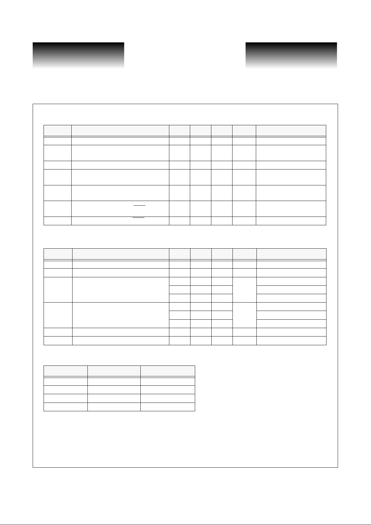
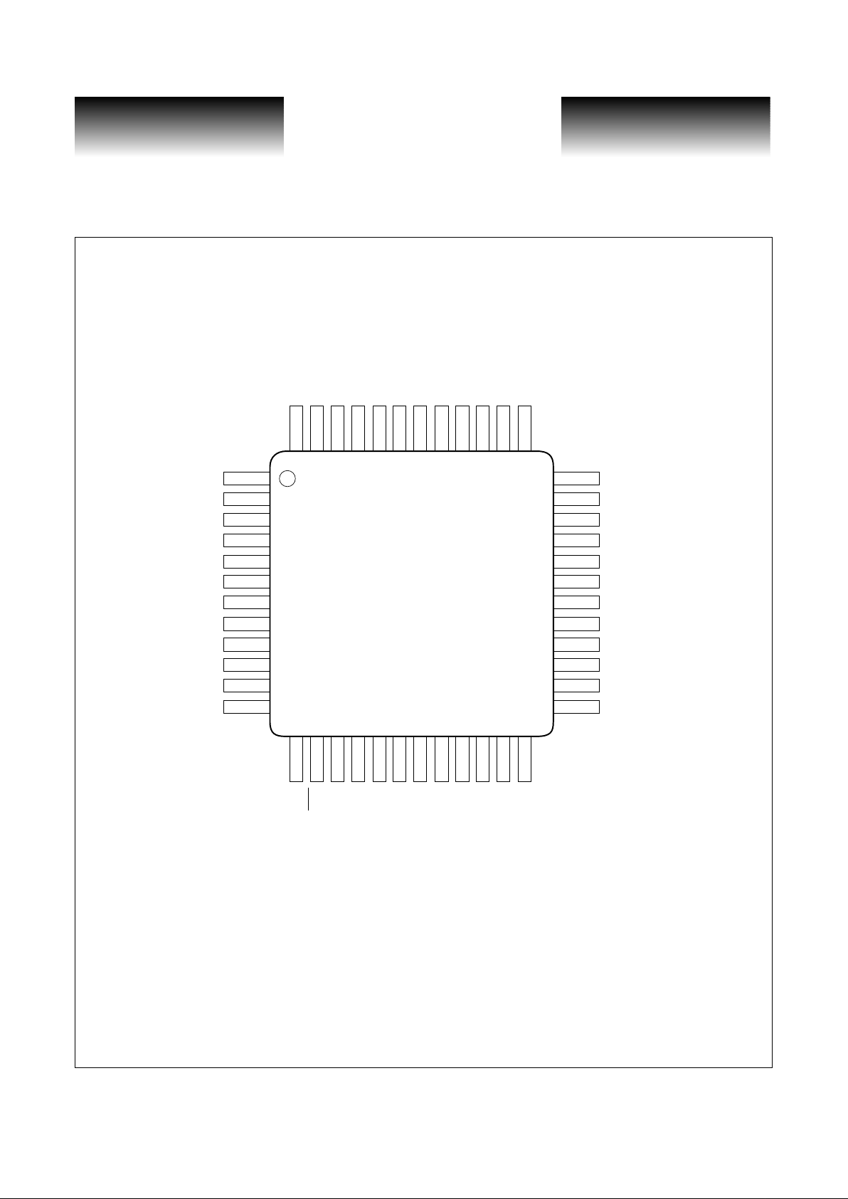
Package Pin Descriptions
Figure 1: Pin Diagram
1
2
3
4
5
6
7
8
9
10
11
12
GND
SQUELCH
VCCA
GND
CZ1
CZ2
GND
GND
IN+
IN-
GND
LEVEL
BIASMON
MODMON
GND
BIASMAX
MODSET
VCC
GND
RESERVED
APCSET_MD
CAPC
NC
ENABLE
13
14
15
16
17
18
19
20
21
22
23
24
TH
LOS
LOS
GND
GND
BIAS
VCC
OUT+
OUT-
VCC
GND
DISABLE
48
47
46
45
44
43
42
41
40
39
38
37
VCC
LAO+
LAO-
VCC
GND
VCC
GND
GND
VCC
DATA-
DATA+
VCC
36
35
34
33
32
31
30
29
28
27
26
25
VSC7962
Page 7
VITESSE
SEMICONDUCTOR CORPORATION
Advance Product Information
VSC7962
3.125Gb/s PECL Limiting Amplifi er with LOS Detect
and Laser Driver with Automatic Powe r Control
G52361-0, Rev 2.1 Page 7
05/01/01
© VITESSE SEMICONDUCTOR CORPORATION • 741 Calle Plano • Camarillo, CA 93012
Tel: (800) VITESSE • FAX: (805) 987-5896 • Email: prodinfo@vitesse.com
Internet: www.vitesse.com
Table 8: Pin Description
Pin Name Pad Name
Pin/Pad
Number
Section Description
GND
GNDA or
GND
1, 4, 7, 8,
11, 16,
17, 23,
30, 34,
41, 42, 44
Both Ground
VCC VCC or VCCA
3, 19, 22,
31, 37,
40, 43,
45, 48
Both 3.3V Supply
SQUELCH SQ 2
Limiting
Amplifier
Squelch Input. Squelch is disabled if this pin in unconnected or
set low. When SQUELCH is high, OUT+ and OUT- are forced
to static levels. See Detailed Description section.
CZ1 CZ1 5
Limiting
Amplifier
Offset Correction Loop Capacitor. Place capacitor between this
pin and CZ2 to alter time con s ta nt of offset correction loop.
See Detailed Description section.
CZ2 CZ2 6
Limiting
Amplifier
Offset Correction Loop Capacitor. Place capacitor between this
pin and CZ1 to alter time con s ta nt of offset correction loop.
See Detailed Description section.
IN+ LAINP 9
Limiting
Amplifier
Noninverted Limiting Amplifier Input Signal
IN- LAINM 10
Limiting
Amplifier
Inverted Limiting Amplifier Input Signal
LEVEL LVL 12
Limiting
Amplifier
Output Current Level. This pin may be either connected to
GND or left unconnected. Connecting to GND causes output
current to be 20mA. The output is 1 6mA when unconnected.
See Detailed Description section.
TH TH 13
Limiting
Amplifier
Loss of Signal (LOS) Threshold. Connect a resistor from this
pin to GND to set the input signal level at which LOS outputs
will be asserted. See Applications Information section.
LOS
LOS 14
Limiting
Amplifier
Inverted Loss of Signal Output. LOS
is high for input signals
above the threshold programmed by TH. See Detailed
Description section.
LOS LOS 15
Limiting
Amplifier
Noninverted Loss-of -Signal Output. LOS i s low for input
signals above the thre shold programmed by TH. See Detailed
Description section.
BIAS BIAS 18
Laser
Driver
Laser Bias current output
OUT+ OUT+ 20
Laser
Driver
Noninverted Laser Modulation Current Output. I
MOD
flows
when input data is high.
OUT- OUT- 21
Laser
Driver
Inverted Laser Modulation Current Output. I
MOD
flows when
input data is low.
Page 8

VITESSE
SEMICONDUCTOR CORPORATION
Advance Product Information
VSC7962
3.125Gb/s PECL Limiting Amplifier with LOS Detect
and Laser Driver with Automatic Power Control
Page 8 G52361-0, Rev 2.1
05/01/01
© VITESSE SEMICONDUCTOR CORPORATION • 741 Calle Plano • Camarillo, CA 93012
Tel: (800) VITESSE • FAX: (805) 987-5896 • Email: prodinfo@vitesse.com
Internet: www.vitesse.com
DISABLE DISABLE 24
Laser
Driver
Disable Input (TTL/CMOS). If used, leave ENABLE pin
floating. Connect to GND for normal operation and V
CC
to
disable laser bias and modulation currents.
ENABLE ENABLE 25
Laser
Driver
Enable Input (TTL/CMOS). If used, connect DISABLE to
GND. Connect to VCC for normal operation and GND to
disable laser bias and modulation currents.
FAIL
FAIL 26
Laser
Driver
Output (TTL/CMOS). When low, indicates APC failure.
CAPC CAPC 27
Laser
Driver
Capacitor to GND sets dominant pole of the APC feedback
loop.
APCSET_MD APCSET_MD 28
Laser
Driver
APCSET and Monitor Diode Input. Resistor to GND sets
desired average laser optical power. If APC is not used connect
100kΩ resistor to GND. Connect to monitor photodiode anode.
Connect capacitor to ground to filter high-speed AC monitor
photocurrent.
RESERVED AUTSEL 29
Laser
Driver
Do not connect.
MODSET MODSET 32
Laser
Driver
Connect resistor to GND to set desired laser modulation
current.
BIASMAX BIASMAX 33
Laser
Driver
Connect resistor to GND to set maximum laser bias current.
The APC function ca n subtract from this value, but it cannot
add to it.
MODMON MODMON 35
Laser
Driver
Modulation current monitor. Sink current source that is
proportional to the laser modulation current.
BIASMON BIASMON 36
Laser
Driver
Bias current monitor . Si nk curren t source that is p roportional to
the laser bias current.
DATA+ DATA+ 38
Laser
Driver
Laser Driver Noninverted Data Input (PECL)
DATA- DATA- 39
Laser
Driver
Laser Driver Inverted Data Input (PECL)
LAO- LAOM 46
Limiting
Amplifier
Inverted Limiting Amplifier Data Output (PECL)
LAO+ LAOP 47
Limiting
Amplifier
Noninverted Limiting Amplifier Data Output (PECL)
Pin Name Pad Name
Pin/Pad
Number
Section Description
Page 9

VITESSE
SEMICONDUCTOR CORPORATION
Advance Product Information
VSC7962
3.125Gb/s PECL Limiting Amplifi er with LOS Detect
and Laser Driver with Automatic Powe r Control
G52361-0, Rev 2.1 Page 9
05/01/01
© VITESSE SEMICONDUCTOR CORPORATION • 741 Calle Plano • Camarillo, CA 93012
Tel: (800) VITESSE • FAX: (805) 987-5896 • Email: prodinfo@vitesse.com
Internet: www.vitesse.com
Bare Die Pad Information
Die Size Not Including Scribe: 2076µm x 2740µm (0.08174” x 0.10788”)
Scribe Size: 157µm (0.00618”)
Pad Passivation Opening: 95µm x 95µm (0.00374” x 0.00374”)
Pad Pitch: 130µm
Die Thickness: 625µm (0.02461”)
The back side of the die may be either left floating or connected to ground.
VCC
DATA+
DATA-
VCC
GND
GND
VCC
GNDA
VCCA
LAOM
LAOP
VCCA
GNDA
SQ
VCCA
GNDA
CZ1
CZ2
GNDA
GNDA
LAINP
LAINM
GNA
LVL
(1)
(2)
(3)
(4)
(5)
(6)
(7)
(8)
(9)
(10)
(11)
(12)
BIASMON
MODMON
GND
BIASMAX
MODSET
VCC
GND
AUTSEL
APCSET_MD
CAPC
FAIL
ENABLE
(36)
(35)
(34)
(33)
(32)
(31)
(30)
(29)
(28)
(27)
(26)
(25)
DISABLE
GND
VCC
OUT-
OUT+
VCC
BIAS
GNDA
GNDA
LOS
LOS
TH
(37)
(38)
(39)
(40)
(41)
(42)
(43)
(44)
(45)
(46)
(47)
(48)
(24)
(23)
(22)
(21)
(20)
(19)
(18)
(17)
(16)
(15)
(14)
(13)
VSC7939
VSC7962
Page 10

VITESSE
SEMICONDUCTOR CORPORATION
Advance Product Information
VSC7962
3.125Gb/s PECL Limiting Amplifier with LOS Detect
and Laser Driver with Automatic Power Control
Page 10 G52361-0, Rev 2.1
05/01/01
© VITESSE SEMICONDUCTOR CORPORATION • 741 Calle Plano • Camarillo, CA 93012
Tel: (800) VITESSE • FAX: (805) 987-5896 • Email: prodinfo@vitesse.com
Internet: www.vitesse.com
Table 9: Pad Coordinates
Pad Name Pin Name
Pad/Pin
Number
Section
X-Coordinate
(µm)
Y-Coordinate
(µm)
GNDA GND 1 Limiting Amplifier 322.500 80.950
SQ SQUELCH 2 Limiting Amplifier 452.500 80.950
VCCA VCC 3 Limiting Amplifier 582.500 80.950
GNDA GND 4 Limiting Amplifier 712.500 80.950
CZ1 CZ1 5 Limiting Amplifier 842.500 80.950
CZ2 CZ2 6 Limiting Amplifier 972.500 80.950
GNDA GND 7 Limiting Amplifier 1102.500 80.950
GNDA GND 8 Limiting Amplifier 1232.500 80.950
LAINP IN+ 9 Limiting Amplifier 1362.500 80.950
LAINM IN- 10 Limiting Amplifier 1492.500 80.950
GNDA GND 11 Limiting Amplifier 1622.500 80.950
LVL LEVEL 12 Limiting Amplifier 1752.500 80.950
TH TH 13 Limiting Amplifier 1995.050 324.475
LOS
LOS 14 Limiting Amplifier 1995.050 514.475
LOS LOS 15 Limiting Amplifier 1995.050 704.475
GNDA GND 16 Laser Driver 1995.050 894.475
GNDA GND 17 Laser Driver 1995.050 1084.475
BIAS BIAS 18 Laser Driver 1995.050 1274.475
VCC VCC 19 Laser Driver 1995.050 1464.475
OUT+ OUT+ 20 Las er Driv er 1995.050 1654.475
OUT- OUT- 21 Laser Driver 1995.050 1844.475
VCC VCC 22 Laser Driver 1995.050 2034.475
GND GN D 23 Laser Driver 1995.050 2224.475
DISABLE DISABLE 24 Laser Driver 1995.050 2414.475
ENABLE ENABLE 25 Laser Driver 1752.500 26 59.050
FAIL
FAIL 26 Laser Driver 1622. 500 2659.050
CAPC CAPC 27 Laser Driver 1492.500 2659.050
APCSET_MD APCSET_MD 28 Laser Driver 1362.500 2659.050
AUTSEL RESERVED 29 Laser Dr iver 1232.50 0 2659.050
GND GND 30 Laser Driver 1102.500 2659.0 50
VCC VCC 31 Laser Driver 972.500 2659.050
MODSET MODSET 32 L a ser Driver 842.500 2659.050
BIASMAX B IASMAX 33 Laser Dr iver 712.500 2659.050
GND GN D 34 Laser Driver 582.500 2659.050
MODMON MODMON 35 Laser Driver 452.500 2659.050
BIASMON B IASMON 36 Laser Driver 322.500 2659.050
Page 11

VITESSE
SEMICONDUCTOR CORPORATION
Advance Product Information
VSC7962
3.125Gb/s PECL Limiting Amplifi er with LOS Detect
and Laser Driver with Automatic Powe r Control
G52361-0, Rev 2.1 Page 11
05/01/01
© VITESSE SEMICONDUCTOR CORPORATION • 741 Calle Plano • Camarillo, CA 93012
Tel: (800) VITESSE • FAX: (805) 987-5896 • Email: prodinfo@vitesse.com
Internet: www.vitesse.com
VCC VCC 37 Laser Driver 80.975 2414.475
DATA+ DATA+ 38 Laser Driver 80.975 2224.475
DATA- DATA- 39 Laser Driver 80.975 2034.475
VCC VCC 40 Laser Driver 80.975 1844.475
GND GND 41 Laser Driver 80.975 1654.475
GND GND 42 Laser Driver 80.975 1464.475
VCC VCC 43 Laser Driver 80.975 1274.475
GNDA GND 44 Limiting Amplifier 80.975 1084.475
VCCA VCC 45 Limiting Amplifier 80.975 894.475
LAOM LAO- 46 Limiting Amplifier 80.975 704.475
LAOP LAO+ 47 Limiting Amplifier 80.975 514.475
VCC VCC 48 Limiting Amplifier 80.975 324.475
Pad Name Pin Name
Pad/Pin
Number
Section
X-Coordinate
(µm)
Y-Coordinate
(µm)
Page 12

VITESSE
SEMICONDUCTOR CORPORATION
Advance Product Information
VSC7962
3.125Gb/s PECL Limiting Amplifier with LOS Detect
and Laser Driver with Automatic Power Control
Page 12 G52361-0, Rev 2.1
05/01/01
© VITESSE SEMICONDUCTOR CORPORATION • 741 Calle Plano • Camarillo, CA 93012
Tel: (800) VITESSE • FAX: (805) 987-5896 • Email: prodinfo@vitesse.com
Internet: www.vitesse.com
Detailed Description
The VSC7962 is a combination limiting amplifier and high-speed laser driver with Automatic Power Control (APC). The device is designed to operate up to 3.125Gb/s with a 3.3V supply. The limiting amplifier provides Loss of Signal (LOS) detect, output offset correction, and output squelch. The limiting amplifier of the
VSC7962 has PECL outputs. The VSC7962 is identical to the VSC7960 except with CML limiting amplifier
outputs. The laser driver data and clock inputs support PECL inputs as well as other inputs that meet the common mode voltage and different i al vol tage swin g specifi cat ions. Th e differential pair output laser driver stage is
capable of driving up to 60mA into the laser with typical rise and fall times of 60ps. To allow for larger output
swings, the VSC7962 was designed to be AC-coupled to the laser cathode with a pull-up inductor for DC-biasing. This configuration will isolate laser forward voltage from the output circuitry and will allow the output at
OUT+ to swing above and below the supply voltage V
CC
. The laser driver output bias and modulation currents
may be easily controlled via external circuitry. The key features of the VSC7962 are Automatic Power Control,
Loss of Signal detect, low power supply current, and fast rise and fall times.
Figure 2: Limiting Amplifier Block Diagram
100
Ω
IN+
IN-
RMS Power
Detect and
Control
Lowpass Filter
10pF
Offset Correction
8k
Ω
Output Control
8k
Ω
V
CC
V
CC
LOS
SQUELCH
LEVEL
OUT+
OUT-
LOS
CZ1 CZ2
TH
Page 13

VITESSE
SEMICONDUCTOR CORPORATION
Advance Product Information
VSC7962
3.125Gb/s PECL Limiting Amplifi er with LOS Detect
and Laser Driver with Automatic Powe r Control
G52361-0, Rev 2.1 Page 13
05/01/01
© VITESSE SEMICONDUCTOR CORPORATION • 741 Calle Plano • Camarillo, CA 93012
Tel: (800) VITESSE • FAX: (805) 987-5896 • Email: prodinfo@vitesse.com
Internet: www.vitesse.com
Figure 3: Laser Driver Block Diagram
Limiting Amplifier Squelch
Squelch is disabled when SQUELC H is not connect ed or is set to TTL lo w level. Wh en SQUELCH is set t o
TTL high level and LOS is asserted, the data outputs, OUT+ and OUT- are forced to static levels. If LOS is not
asserted, the outputs will not be squelched.
Limiting Amplifier Loss of Signal (LOS) Detect
This features utilizes an RMS power detector with prog rammable LOS indicator to provid e two outputs,
LOS and LOS
. The input TH is used to set the threshold at which the loss of signal detector outputs, LOS and
LOS,
change state. See Loss-of-Signal Specifications table (Table 6) for setting the resistor value between TH
and ground. The Loss of Signal Truth Table (Table 7) clarifies how LOS and SQUELCH interact.
Limiting Amplifier Offset Correction
This feature is provided to ensure that the offsets in the limiting amplifier coupled with its gain do not cause
the output buffer to give a false output. Because of the high gain of the amplifier, offset correction using a lowfrequency feedback loop reduces input offset. If no comp onent is placed between pins CZ1 an d CZ2, the low
frequency cut-off is 2MHz. If a 0.1
µF capacitor is placed between CZ1 and CZ 2, the low frequency cut-off is
lowered to approximately 2kHz. For Fibre Channel and Gigabit Ethernet applications, leave pins CZ1 and CZ2
open. For ATM/SONET and other scrambled non-return-to-zero (NRZ) applications, place a 0.1
µF capacitor
between CZ1 and CZ2. This maintains a one-d ecade separat ion bet ween t he lo west inpu t frequ ency and t he low
frequency cut-off. The low frequency cut-off of the offset correction loop is given by the following equation:
f
OC
= 43 / [2π * 35k (CZ + 100pF)]
= 196* 10
-6
/ (CZ + 100pF)
= 196* 10
-6
/ (0.1µF + 100pF)
= 1.96kHz
MUX
DATA+
APC
DATA-
ENABLE
BIAS
IOUT+
IOUT-
MODSET BIASMAX CAPC
APCSET_MD
C
D
L
P
V
CC
L
P
1nF
V
CC
C
F
R
F
MODMON
V
CC
BIASMON
V
CC
DISABLE
FAIL
Page 14

VITESSE
SEMICONDUCTOR CORPORATION
Advance Product Information
VSC7962
3.125Gb/s PECL Limiting Amplifier with LOS Detect
and Laser Driver with Automatic Power Control
Page 14 G52361-0, Rev 2.1
05/01/01
© VITESSE SEMICONDUCTOR CORPORATION • 741 Calle Plano • Camarillo, CA 93012
Tel: (800) VITESSE • FAX: (805) 987-5896 • Email: prodinfo@vitesse.com
Internet: www.vitesse.com
Figure 4: Supply Current Measurement
Laser Driver Automatic Power Control
To ensure constant average optical pow er, the device utilizes an Automatic Power Control loop (APC). A
photodiode mounted in the laser package provides optical feedback to compensate for changes in average laser
output power due to changes that affect laser performance such as temperature and laser lifetime. The laser bias
current is adjusted by the APC loop according t o the reference current set at APCSET_MD b y an ex tern al re sistor. An external capacitor at CAPC controls the time constant for the APC feedback loop. The recommended
value for CAPC is 0.1µF. This value reduces pattern-dependent jitter associated with the APC feedback loop
and guarantees stability. If the APC loop cannot adjust the bias current to track the desired monitor current,
FAIL
is set low.
The device may be operated with or without APC. To utilize APC, a capacitor must be connected at CAPC
(0.1µF) and a resistor must be conne cted at APCSET_MD to set the average optical power. For open-loop operation (no APC), a 100k
Ω resistor should be connected between APCSET_MD and GND. CAPC has no effect
on open-loop operation. In both modes of operation, resistors to ground should be placed at BIASMAX and
MODSET to set the bias and modulation currents.
I
MOD
V
CC
I
CC
VSC7959
I
OUT
100
Ω
100
Ω
Supply Current (ICC and IEE)
A
100
Ω
100
Ω
V
EE
A
I
EE
Page 15

VITESSE
SEMICONDUCTOR CORPORATION
Advance Product Information
VSC7962
3.125Gb/s PECL Limiting Amplifi er with LOS Detect
and Laser Driver with Automatic Powe r Control
G52361-0, Rev 2.1 Page 15
05/01/01
© VITESSE SEMICONDUCTOR CORPORATION • 741 Calle Plano • Camarillo, CA 93012
Tel: (800) VITESSE • FAX: (805) 987-5896 • Email: prodinfo@vitesse.com
Internet: www.vitesse.com
Laser Driver Short-Circuit Protection
If BIASMAX or MODSET are shorted to ground, the output mo dulation and bias currents will be turned
off.
Laser Driver Enable/Disable
Two pins are provided to allow either ENABLE or DISABLE control. If ENABLE is used, connect disable
to ground. If DISABLE is used, leave ENA BLE floating. Both modulation and bias currents are turned off
when ENABLE is low or DISABLE is high. Typically, ENABLE or DISABLE responds within approximately
250ns.
Controlling the Laser Driver Modulation Current
The output modulation current may be determined from the following equation where P
p-p
is peak-to-peak
optical power, P
AVE
is average power, r
e
is extinction ratio, and η is laser slope efficiency:
I
MOD
= P
p-p
/ η= 2 * P
AVE
* (re-1) / (re+1) / η
A resistor at MODSET controls the output bias current. Graphs of I
MODSET
vs. R
MODSET
in Typical Operat-
ing Characteristics describe the relationship between the resistor at MODSET and the output modulation current at 25
°C. After determining the desired output modulation current, use the graph to determine the
appropriate resistor value at MODSET.
Controlling the Laser Driver Bias Current
A resistor at BIASMAX should be used to control t he outpu t bias current . Graphs of I
BIASMAX
Vs. R
BIASMAX
in Typical Operating Characte rist i cs describ e the relationshi p between the resistor at BIASMAX and the out put
bias current at 25
°C. If the APC is not used, the appropriate resistor value at BIASMAX is determined by first
selecting the desired output bias current, and then using the graph to determine the appropriate resistor value at
BIASMAX. When using APC, BIASMAX sets the maximum allowed bias current. After determining the maximum end-of-life bias current at 85
°C for the laser, refer to the graph of I
BIASMAX
Vs. R
BIASMAX
in T ypi cal Oper-
ating Characteristics to select the appropriate resistor value.
Controlling the Laser Driver APC Loop
To select the resistor at APCSET_MD, use the graph of IMD vs. R
APCSET
in Typical Operating Characteris-
tics. The graph relates the desired monitor current to the appropriate resistance value at APCSET_MD. I
MD
may
be calculate from the de sired optical average power, P
AVE,
, and the laser-to-monitor transfer , ρ
MON
, for a specific
laser using the following equation:
I
MD
= P
AVE
* ρ
MON
Laser Diode Interface
An RC shunt network should be placed at the laser outpu t interface. Th e sum of the resistor placed at the
output and the laser diode resistance should be 25
Ω. For exam ple, if th e lase r diode ha s a resis tance o f 5Ω, a
Page 16

VITESSE
SEMICONDUCTOR CORPORATION
Advance Product Information
VSC7962
3.125Gb/s PECL Limiting Amplifier with LOS Detect
and Laser Driver with Automatic Power Control
Page 16 G52361-0, Rev 2.1
05/01/01
© VITESSE SEMICONDUCTOR CORPORATION • 741 Calle Plano • Camarillo, CA 93012
Tel: (800) VITESSE • FAX: (805) 987-5896 • Email: prodinfo@vitesse.com
Internet: www.vitesse.com
20Ω resistor should be placed in series with the laser. For optimal performance, a bypass capacitor should be
placed close to the laser anode.
A “snubber network” consisting of a capacitor C
F
and resistor RF should be placed at the laser output to
minimize reflections fro m the laser (see Blo ck Diagram , page 1). Sugg ested values for these compon ents are
80
Ω and 2pF, respectively . Howeve r, these values should be adjusted u ntil a su it able o pt ical o ut put waveform is
obtained.
Reducing Pattern-Dependent Jitter
Three design values significantly affect pattern-dependent jitter: the capacitor at CAPC, the pull-up induc-
tor at the output (L
P
), and the AC-coupling ca paci tor at t he out pu t ( CD). As previously stated, the recommended
value for the capacitor at CAPC is 0.1
µF. This results in a 10kHz loop bandwidth which makes the pattern-
dependent jitter from the APC loop negligible.
For 2.5Gb/s data rates, the recommended value for C
D
is 0.056µF. The time constant at the output is domi-
nated by L
P
. The variation in the peak vol tage sho ul d be l ess that 12% of t he averag e vol t age over the maxi mum
consecutive identical digit (CID) period. The following equation approximates this time constant for a CID
period, t, of 100UI = 40ns:
τ
LP
= -t / ln(1-12%) = 7.8t = LP / 25Ω
Therefore, the inductor LP should be a 7.8µH SMD ferrite bead inductor for this case.
Input/Output Considerations
Although the VSC7962 laser dr iver is P ECL-c o mpat ib le, this i s not req uire d to dr iv e the device. The inputs
must only meet the common-mode voltage and differential voltage swing specifications.
Laser Driver Power Consumption
The following equation provides the device supply current (IS) in terms of quiescent current (IQ), modula-
tion current (I
MOD
), and bias current (I
BIAS
):
I
S
= IQ + 0.47 * I
MOD
+ 0.15 * I
BIAS
For 3.3V operation, IQ is 15mA.
This equation may be used to determine the estimated power dissipation:
P
DIS
= VCC * I
S
For example, the device operated at 3.3V with a 30mA modulation current and a 10mA bias current would
have a supply current of:
I
S
= 15mA + 0.47 * 30mA + 0.15 * 10mA = 31mA
This corresponds to a power dissipation of 3.3V * 31mA = 102mW.
Page 17

VITESSE
SEMICONDUCTOR CORPORATION
Advance Product Information
VSC7962
3.125Gb/s PECL Limiting Amplifi er with LOS Detect
and Laser Driver with Automatic Powe r Control
G52361-0, Rev 2.1 Page 17
05/01/01
© VITESSE SEMICONDUCTOR CORPORATION • 741 Calle Plano • Camarillo, CA 93012
Tel: (800) VITESSE • FAX: (805) 987-5896 • Email: prodinfo@vitesse.com
Internet: www.vitesse.com
Typical Operating Characteristics
I
MODSET
vs. R
MODSET
T=25°C, VCC = 3.3V
I
BIASMAX
vs. R
BIASMAX
T=25°C, VCC = 3.3V
IMD vs. R
APCSET
,
T=25°C, VCC = 3.3V
Rise and Fall Times
T=85°C, VCC = 3.3V
Page 18

VITESSE
SEMICONDUCTOR CORPORATION
Advance Product Information
VSC7962
3.125Gb/s PECL Limiting Amplifier with LOS Detect
and Laser Driver with Automatic Power Control
Page 18 G52361-0, Rev 2.1
05/01/01
© VITESSE SEMICONDUCTOR CORPORATION • 741 Calle Plano • Camarillo, CA 93012
Tel: (800) VITESSE • FAX: (805) 987-5896 • Email: prodinfo@vitesse.com
Internet: www.vitesse.com
Applications Information
The following is a typical design example for the laser driver of the VSC7962 assuming 3.3V operation
with APC.
Select a Laser
The following table provides specifications for a typical commun ica tion-g rade la ser capable of operating at
2.5 Gb/s.
Table 10: Typical Laser Characteristics
Select Resistor for APCSET_MD
The monitor diode current is estimated by IMD = P
AVE
* ρ
MON
= 6mW * 0.04mA/mW = 0.24mA. The IMD
vs. R
APCSET
in Typical Operating Characteristics shows the resistor at APCSET_MD should be 5kΩ.
Monte Carlo Simulation of I
CC
Symbol Parameter Value Units
λ Wavelength 1310 nm
P
AVE
Average Optical Output Power 6 mW
I
th
Threshold Current 6 mA
ρ
MON
Laser to Monitor Transfer 0.04 mA/mW
η Laser Slope Efficiency 0.4 mW/mA
T
C
Operating Temperature Range -40 to +85 °C
Page 19

VITESSE
SEMICONDUCTOR CORPORATION
Advance Product Information
VSC7962
3.125Gb/s PECL Limiting Amplifi er with LOS Detect
and Laser Driver with Automatic Powe r Control
G52361-0, Rev 2.1 Page 19
05/01/01
© VITESSE SEMICONDUCTOR CORPORATION • 741 Calle Plano • Camarillo, CA 93012
Tel: (800) VITESSE • FAX: (805) 987-5896 • Email: prodinfo@vitesse.com
Internet: www.vitesse.com
Select Resistor for MODSET
T o ensure some minimum extinction ratio over temperature and lifetime, assume an optimal extinction ratio
of 20 (13dB) at 25
°C. The modulation current may be calculated from the following equation:
I
MOD
= P
p-p
/ η= 2 * P
AVE
* (re-1) / (re+1) / η = 2 * 6mA * (20-1) / (20 + 1) / 0.4 = 27.1mA
The graph of I
MODSET
vs. R
MODSET
in Typical Operating Characteristics shows the resistor for MODSET
should be 8.5k
Ω.
Select Resistor for BIASMAX
The maximum threshold current at +85°C and end-of-life must be determined. A graph of a typical laser’s
I
th
versus TC reveals a maximum threshold current of 30mA at 85°C. Therefore, the maxim um bias can be
approximated by:
I
BIASMAX
= I
TH-MAX
+ I
MOD
/ 2 = 30mA + 27.1mA / 2 = 43.6mA
The graph of I
BIASMAX
vs. R
BIASMAX
in T ypi ca l Operating Characteristics shows the resistor for BIASMAX
should be 5k
Ω.
Wire Bonding
For best performance gold ball-bonding techniques are recommended. Wedge bonding is not recom-
mended. For best performance and to minimize inductance keep wire bond lengths short.
PCB Layout Guidelines
Use high frequency PCB layout techniques with solid ground planes to minimize crosstalk and EMI. Keep
high speed traces as short as possible for signal integrity. The output traces to the laser diode must be short to
minimize inductance. Short output traces will provide best performance.
Page 20

VITESSE
SEMICONDUCTOR CORPORATION
Advance Product Information
VSC7962
3.125Gb/s PECL Limiting Amplifier with LOS Detect
and Laser Driver with Automatic Power Control
Page 20 G52361-0, Rev 2.1
05/01/01
© VITESSE SEMICONDUCTOR CORPORATION • 741 Calle Plano • Camarillo, CA 93012
Tel: (800) VITESSE • FAX: (805) 987-5896 • Email: prodinfo@vitesse.com
Internet: www.vitesse.com
Package Information - 48-pin TQFP
1. All dimensioning and tolerancing conform to ANSI Y14.5-1982.
2. Controlling dimension: millimeter.
3. This outline conforms to JEDEC Publication 95 Registration MS-026.
Page 21

VITESSE
SEMICONDUCTOR CORPORATION
Advance Product Information
VSC7962
3.125Gb/s PECL Limiting Amplifi er with LOS Detect
and Laser Driver with Automatic Powe r Control
G52361-0, Rev 2.1 Page 21
05/01/01
© VITESSE SEMICONDUCTOR CORPORATION • 741 Calle Plano • Camarillo, CA 93012
Tel: (800) VITESSE • FAX: (805) 987-5896 • Email: prodinfo@vitesse.com
Internet: www.vitesse.com
Ordering Informatio n
The order number for this product is formed by a combination of the device type and package type.
Notice
Vitesse Semiconductor Corporation (“Vitesse”) provides this document for informational purposes only. This document contains pre-production
information about Vitesse products in their conce pt, development and/or testing phase. All informaiton in this document, including descri ptions of
features, functions, performan ce, technical specifications and availability, is s ubject to change without notice at any time. Nothing contained in this
document shall be co nstru ed as e xten ding an y w arran ty or pr omise , e xpress or imp lied , that any Vitesse product wi ll b e av ail able as described or
will be suitable for or will accompli sh any particular task.
Vitesse products are not intended for use in life support applia nc es, devices or systems. Use of a Vitesse product in such applications without written consent is prohibited. 0
VSC7962
XX
Device T y pe
Package Style:
W : Bare Die in Waffle Pack
3.125Gb/s PECL Limiting Amplifier with LOS Detect
RO : 48-pin TQFP
and Laser Driver with Automatic Power Control
Page 22

VITESSE
SEMICONDUCTOR CORPORATION
Advance Product Information
VSC7962
3.125Gb/s PECL Limiting Amplifier with LOS Detect
and Laser Driver with Automatic Power Control
Page 22 G52361-0, Rev 2.1
05/01/01
© VITESSE SEMICONDUCTOR CORPORATION • 741 Calle Plano • Camarillo, CA 93012
Tel: (800) VITESSE • FAX: (805) 987-5896 • Email: prodinfo@vitesse.com
Internet: www.vitesse.com
 Loading...