

Page 1
VITESSE
SEMICONDUCTOR CORPORATION
Advance Product Information
VSC7959
3.125Gb/s CML Limiting Amplifier with LOS Detect
Features Applications
• 3.3V or 5V Power Supply
• Typical Supply Current of 32mA
• Current-Mode Logic Outputs
• Optional Output Squelch
• Loss of Signal Detect
• Output Offset Correction
• Rise/Fall Times Faster than 100ps
• Packages: TSSOP-16, Bare Die
• SONET/SDH at 622Mb/s, 1.244Gb/s, 2.488Gb/s,
and 3.125Gb/s
• Full-Speed Fibre Channel (1.062Gb/s)
• Small Form Factor (SFF) Receivers
• ATM Optical Receivers
General Description
The VSC7959 is a single supply limiting amplifier with Loss of Signal (LOS) detect for SONET/SDH and
Fibre Channel applications up to 3.125Gb/s. The VSC7959 provides a constant output signal swing for a wide
range of input voltages a nd h as Current -Mode Logic ( CML) outp uts. Th e VSC796 1 pro vides the same funct ionality as the VSC7959 with positive emitter-coupled logic (PECL) outputs. Key features of the VSC7959 are its
RMS power detectors for programmable LOS detection, optional output squelch, adjustable output levels,
excellent jitter performance, and fast edge rates. The VSC7959 is available in die form or in a TSSOP-16 package.
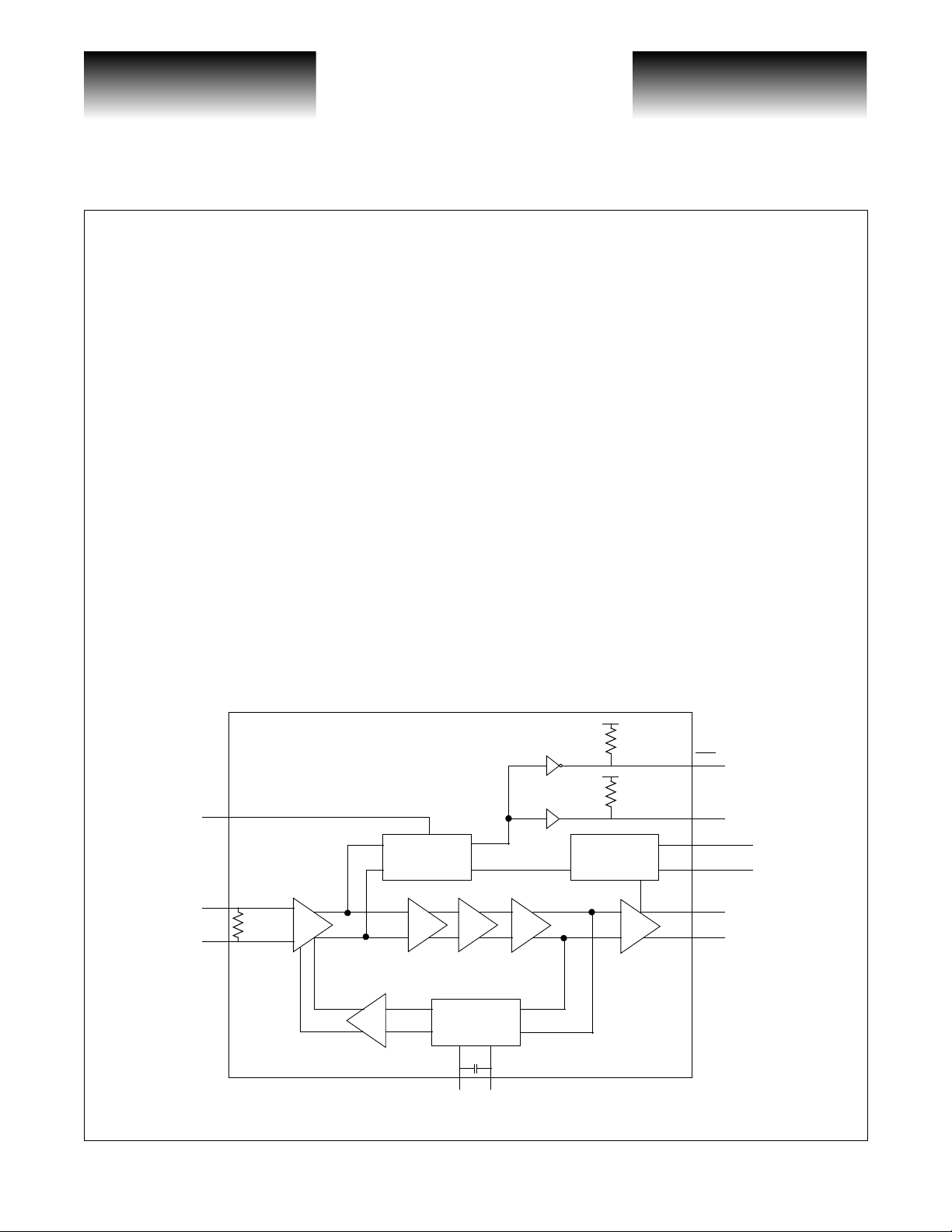
Block Diagram
VSC7959
TH
IN+
100
IN-
V
CC
8k
Ω
LOS
V
CC
8k
Ω
LOS
RMS Power
Detect and
Control
Ω
Lowpass Filter
Offset Correction
10pF
CZ1 CZ2
Output Control
SQUELCH
LEVEL
OUT+
OUT-
G52358-0, Rev 2.0 Page 1
02/09/01
© VITESSE SEMICONDUCTOR CORPORATION • 741 Calle Plano • Camarillo, CA 93012
Tel: (800) VITESSE • FAX: (805) 987-5896 • Email: prodinfo@vitesse.com
Internet: www.vitesse.com
Page 2
VITESSE
SEMICONDUCTOR CORPORATION
Advance Product Information
3.125Gb/s CML Limiting Amplifier with LOS Detect
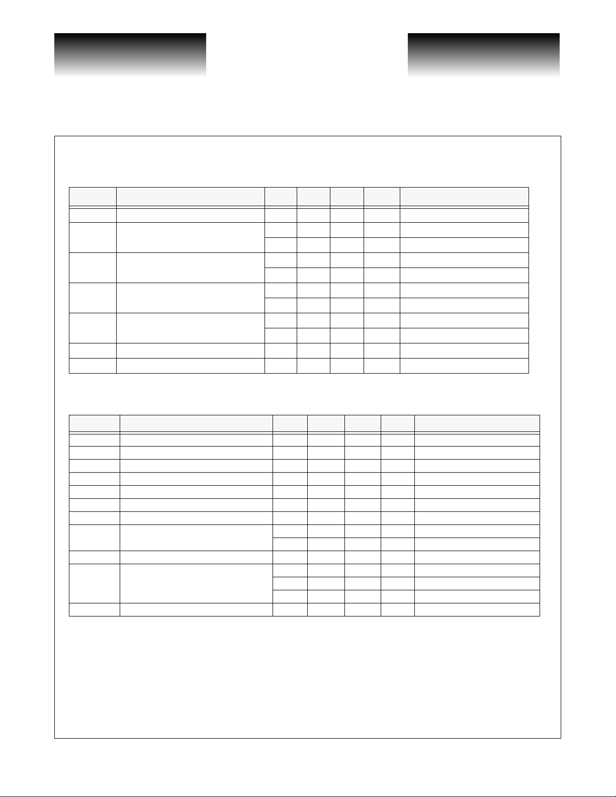
Electrical Characteristics
Table 1: DC Specifications
Symbol Parameter Min Typ Max Units Conditions
V
CC
I
CC
I
EE
I
CCSQ
I
EESQ
I
SQ
PSSR Power Supply Rejection Ratio 20 30 dB f < 2MHz
NOTE: (1) See Figure 5 for supply current measurement setup.
Table 2: DC Specifications
Power Supply Voltage 3.135 5.5 V
Power Supply Current
Power Supply Current
Power Supply Current when
Squelched
Power Supply Current when
Squelched
Squelch Input Current 0 400 µA
(1)
(1)
(1)
(1)
31 mA VCC = 3.3V
35 mA V
38 mA VCC = 3.3V
43 mΑ V
21 mA VCC = 3.3V
25 mA V
24 mA VCC = 3.3V
28 mA V
CC
CC
CC
CC
= 5V
= 5V
= 5V
= 5V
VSC7959
Symbol Parameter Min Typ Max Units Conditions
Data Rate 3.125 Gb/s
V
IN
J
D
J
R
t
R, tF
V
N
R
DIFF
f
L
V
SQ
V
CML
Z
O
NOTES: (1) Deterministic jitter measured peak-to-peak with K28.5 pattern. (2) Random jitter measured with minimum input.
Input V oltage Range 10 1200 mV Peak-to-peak
Deterministic Jitter 25 ps See Note 1
Random Jitter 8 ps See Note 2, RMS
Rise and Fall Times 55 100 ps 20% to 80%
Input Referred Noise 230 µV RMS, IN+ to INDifferential Input Resistance 100 Ω IN+ to IN-
Low Frequency Cutof f
Output Signal When Squelched 20 mV Output AC-coupled
550 1200 mV Level = open, RL = 50Ω
CML Output Voltage
Output Resistance 100 Ω Single-ended
1100 1800 mV Level = GND, RL = 75Ω
2MHzC
2kHzC
20 mV Squelched
open
Z
= 0.1µF
Z
Page 2 G52358-0, Rev 2.0
© VITESSE SEMICONDUCTOR CORPORATION • 741 Calle Plano • Camarillo, CA 93012
Tel: (800) VITESSE • FAX: (805) 987-5896 • Email: prodinfo@vitesse.com
Internet: www.vitesse.com
02/09/01
Page 3
VITESSE
SEMICONDUCTOR CORPORATION
Advance Product Information
VSC7959
3.125Gb/s CML Limiting Amplifier with LOS Detect
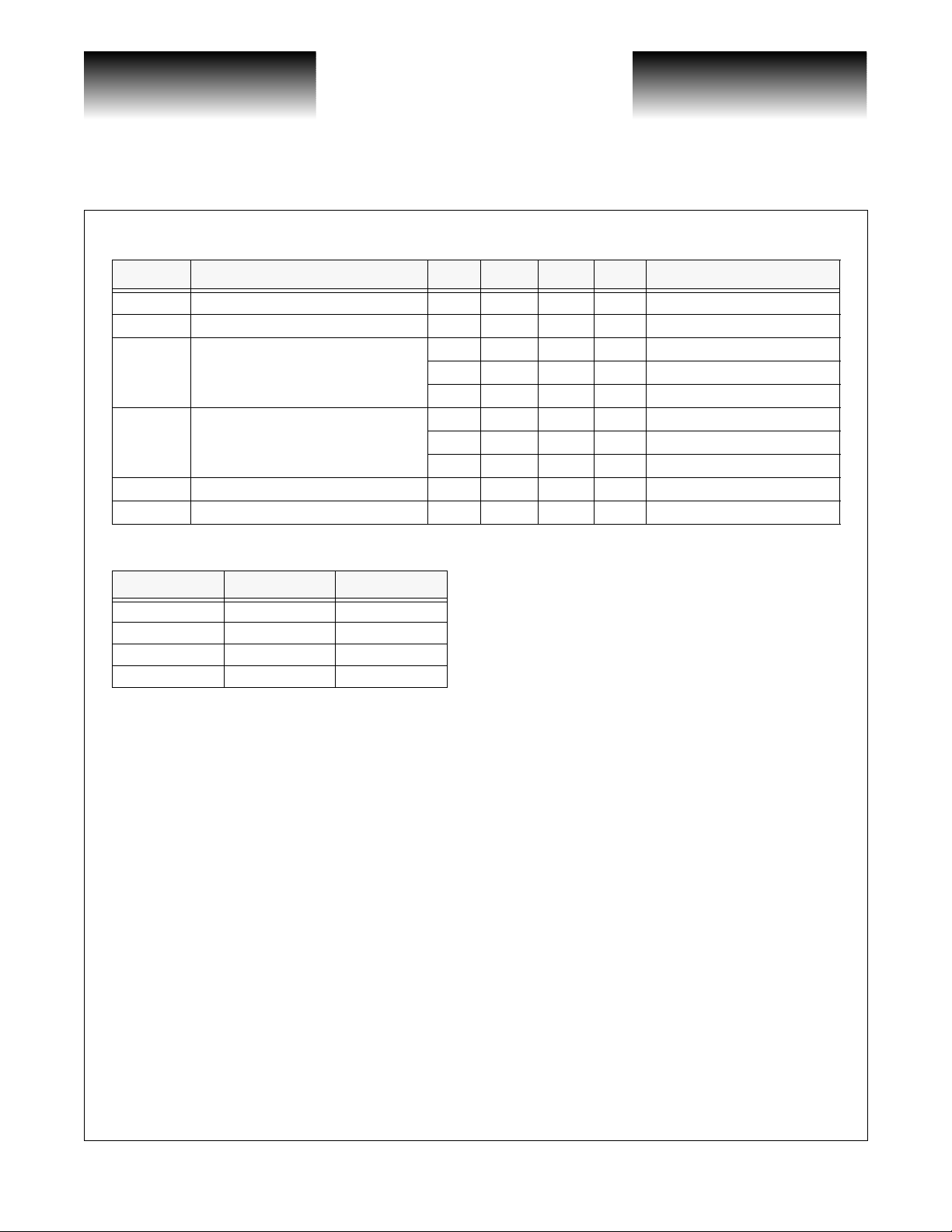
Table 3: Loss of Signal Specifications
Symbol Parameter Min Typ Max Units Conditions
H
I
V
V
V
V
LOS
LOS
THA
THD
LOSH
LOSL
LOS Hystersis 3.1 3.3 5.5 dB H
LOS Assert/Deassert Time 0.22 0.25 0.28 µs
8.2 mV R
LOS Assert Threshold
LOS Deassert Threshold
LOS Output HIGH Volta ge 3.3 V I
LOS Output LOW Voltage 0.168 V I
12.8 19.8 21.8 mV R
57.2 mV R
11.4 mV R
26.2 29.0 31.6 mV R
75.2 mV R
= 20 log (V
LOS
= 2.5kΩ
TH
= 7kΩ
TH
= 20kΩ
TH
= 2.5kΩ
TH
= 7kΩ
TH
= 20kΩ
TH
= –30µA
LOS
= +1.2µA
LOS
Table 4: Loss of Signal Truth Table
SQUELCH LOS Output
High Low Off
Low High On
High Low On
Low Low On
THD/VTHA
)
Absolute Maximum Ratings
(1)
Power Supply Voltage (VCC).............................................................................................................-0.5V to +6V
Maximum Junction Temperature Range .........................................................................................................TBD
Storage Temperature Range (T
NOTE: (1) CAUTION: Stresses listed under “Absolute Maximum Ratings” may be applied to devices one at a time without caus-
ing permanent damage. Functionality at or above the values listed is not implied. Exposure to these values for extended
periods may affect device reliability.
).................................................................................................-55°C to +150°C
S
Recommended Operating Conditions
Positive Voltage Rail (VCC)..................................................................................................................3.3V or 5V
Junction Temperature Range (T
Ambient Temperature Range (T
G52358-0, Rev 2.0 Page 3
02/09/01
© VITESSE SEMICONDUCTOR CORPORATION • 741 Calle Plano • Camarillo, CA 93012
)................................................................................................-40°C to +100°C
J
).................................................................................................-40°C to +85°C
A
Tel: (800) VITESSE • FAX: (805) 987-5896 • Email: prodinfo@vitesse.com
Internet: www.vitesse.com
Page 4

VITESSE
SEMICONDUCTOR CORPORATION
Advance Product Information
3.125Gb/s CML Limiting Amplifier with LOS Detect
Package Pin Descriptions
Figure 1: Pin Diagram
Top Vi ew
TSSOP-16 Package
CZ1
CZ2
GND
IN+
IN-
GND
LEVEL
TH
Table 5: Pin Identifications
Pin Name Pin No. Description
CZ1 1
CZ2 2
GND 3 Supply Ground
IN+ 4 Noninverted Input Signal
IN- 5 Inverted Input Signal
GND 6 Supply Ground
LEVEL 7
TH 8
LOS
LOS 10
VCC 11 Power Supply
OUT- 12 Inverted Data Output
OUT+ 13 Noninverted Data Output
VCC 14 Power Supply
SQUELCH 15
NC 16 No Connection
9
Offset Correction Loop Capacitor. Place capacitor between this pin and CZ2 to alter time constant
of offset correctio n loop. See Detailed Description section.
Offset Correction Loop Capacitor. Place capacitor between this pin and CZ1 to alter time constant
of offset correctio n loop. See Detailed Description section.
Output Current Level. This pin may either be connected to ground or left unconnected. Connecting
to ground causes output current to be 20mA. The output is 16 mA when left unconnected. See
Detailed Description section.
Loss of Signal (LOS) Threshold. Connect a resistor from this pin to ground to set the input signal
level at which LOS outputs will be asserted. See Application Information section.
Inverted Los s of S ign al O utput . LOS is HIG H for inp ut si gnal s ab ove the th res hold pro gram med by
TH. See Detailed Description section.
Noninverted Loss of Signal Ou tput. LO S is LOW f or inpu t signals abov e the thr eshold program med
by TH. See Detailed Description section.
Squelch Input. Squelch is disabled if this pin is unconnected or set LOW. When SQUELCH is
HIGH, OUT+ and OUT- are forced to static levels.
1
2
3
4
5
6
7
8
VSC7959
16
15
14
13
12
11
10
9
VSC7959
NC
SQUELCH
VCC
OUT+
OUTVCC
LOS
LOS
Page 4 G52358-0, Rev 2.0
© VITESSE SEMICONDUCTOR CORPORATION • 741 Calle Plano • Camarillo, CA 93012
Tel: (800) VITESSE • FAX: (805) 987-5896 • Email: prodinfo@vitesse.com
Internet: www.vitesse.com
02/09/01
Page 5

VITESSE
SEMICONDUCTOR CORPORATION
Advance Product Information
VSC7959
Bare Die Descriptions
1597µm
(0.06287")
Pad 2
CAZ2
Pad 3
GNDA
Pad 4
LAINP
Pad 5
LAINM
Pad 6
GNDA
3.125Gb/s CML Limiting Amplifier with LOS Detect
Figure 2: Pad Assignments
1597
µm (0.06287")
Pad1
CAZ1
VSC7959
Pad 16
NC
Pad 15
SQ
Pad 14
VCCA
Pad 13
LAOP
Pad 12
LAOM
Pad 11
VCCA
Pad 7
LVL
Pad 8
TH
Die Size: 1597µm x 1597µm (0.06287" x 0.06287")
Pad Pitch: 180µm (0.00709")
Pad Passivation Opening:
The back side of the die may either be left floating or connected ot ground.
95µm x 95µm (0.00374" x 0.00374")
Pad 9
LOS
Pad 10
LOS
G52358-0, Rev 2.0 Page 5
02/09/01
© VITESSE SEMICONDUCTOR CORPORATION • 741 Calle Plano • Camarillo, CA 93012
Tel: (800) VITESSE • FAX: (805) 987-5896 • Email: prodinfo@vitesse.com
Internet: www.vitesse.com
Page 6

VITESSE
SEMICONDUCTOR CORPORATION
Advance Product Information
3.125Gb/s CML Limiting Amplifier with LOS Detect
Table 6: Pad Coordinates
Pad
Name
CZ1 CZ1 1 270.525 1359.05
CZ2 CZ2 2 80.95 1170.525
GNDA GND 3 80.95 990.525 Supply Ground
LAINP IN+ 4 80.95 810.525 Noninverted Input Signal
LAINM IN- 5 80.95 630.525 Inverted Input Signal
GNDA GND 6 80.95 450.525 Supply Ground
LVL LEVEL 7 80.95 270.525
TH TH 8 270.525 80.95
LOS
LOS LOS 10 1359.05 270.525
VCCA VCC 11 1359.05 450.525 Power Supply
LOAM OUT- 12 1359.05 630.525 Inverted Data Output
LAOP OUT+ 13 1359.05 810.525 Noninverted Data Output
VCCA VCC 14 1359.05 990.525 Power Supply
SQ SQUELCH 15 1359.05 1170.525
— NC —/16 1169.475 1359.05 No Connection
Pin Name
LOS 9 1169.475 80.95
Pad/Pin
Number
Coordinates (µm)
X Y
Offset Correction Loop Capacitor. Place capacitor between
this pin and CZ2 to alter time constant of offset correction
loop. See Detailed Description section.
Offset Correction Loop Capacitor. Place capacitor between
this pin and CZ1 to alter time constant of offset correction
loop. See Detailed Description section.
Output Current Level. This pin may either be connected to
ground or left unconnected. Connect ing to ground causes
output current to be 20mA. The output is 16mA when left
unconnected. See Detailed Description section.
Loss of Signal (LOS) Threshold. Connect a resistor from
this pin to ground to set the input signal level at which LOS
outputs will be asserted. See Application Information
section.
Inverted Loss of Signal Output. LOS is HIGH for input
signals above the thr eshold programmed by TH . See
Detailed Description section.
Noninverted Loss of Signal Output. LOS is LOW for input
signals above the thr eshold programmed by TH . See
Detailed Description section.
Squelch Input. Sque lch is disa bled if thi s pin is unconn ected
or set LOW. When SQUELCH is HIGH, OUT+ and OUTare forced to static levels.
VSC7959
Description
Page 6 G52358-0, Rev 2.0
© VITESSE SEMICONDUCTOR CORPORATION • 741 Calle Plano • Camarillo, CA 93012
Tel: (800) VITESSE • FAX: (805) 987-5896 • Email: prodinfo@vitesse.com
Internet: www.vitesse.com
02/09/01
Page 7

VITESSE
SEMICONDUCTOR CORPORATION
Advance Product Information
VSC7959
3.125Gb/s CML Limiting Amplifier with LOS Detect
Detailed Description
The VSC7959 is a high speed limiting amplifier with Loss-of-Signal (LOS) detect. The device is designed
to operate with a 3.3V or 5V su pply in SDH/SONET and Fibre C hannel applications up to 3.1 25Gb/s. The
VSC7959 has current-mode logic (CML) outputs. The VSC7961 provides the same functionality as the
VSC7959 with positive emitter-coupled logic (PECL) outputs. The key featur es of the V SC7959 are Loss-ofSignal (LOS) detect, output offset correction, output squelch, adjustable output levels, low power supply current, and fast rise and fall times.
The inputs of the device provide 100
coupled. The CML output circuits ar e designed to tolera te output impedanc e mismatches and may be AC- or
DC-coupled.
Loss of Signal (LOS) Detect
This features utilizes an RMS power detector with prog rammable LOS indicator to provid e two outputs,
LOS and LOS
LOS,
change state. See the Loss of Si gnal Sp ecifica tions (Table 3) for setting the resistor value between TH and
ground. The Loss of Signal Truth Table (Table 4) clarifies how LOS and SQUELCH interact.
Optional Squelch
Squelch is disabled when SQUELC H is not conn ected or is set to TTL lo w level. Wh en SQUELCH is set to
TTL high level and LOS is asserted, the data outputs, OUT+ and OUT- are forced to static levels. If LOS is not
asserted, the outputs will not be squelched.
. The input TH is used to set the threshold at which the loss of signal detector outputs, LOS and
Ω input impedance between IN+ and IN- and are intended to be DC-
Offset Correction
This feature is provided to ensure that the offsets in the limiting amplifier coupled with its gain do not cause
the output buffer to give a false output. Because of the high gain of the amplifier, offset correction using a lowfrequency feedback loop reduces input offset. If no comp onent is placed between pins CZ1 an d CZ2, the low
frequency cut-off is 2MHz. If a 0.1
lowered to about 2kHz. For F ibre C hannel and Giga bit E thernet appl icati ons, le ave p ins CZ1 and CZ2 o pen. For
ATM/SONET and other scrambled non-return-to-zero (NRZ) applications, place a 0.1
CZ1 and CZ2. This maintains a one-decade separation between the lowest input frequency and the low frequency cut-off. The low frequency cut-off of the offset correction loop is given by the following equation:
G52358-0, Rev 2.0 Page 7
02/09/01
© VITESSE SEMICONDUCTOR CORPORATION • 741 Calle Plano • Camarillo, CA 93012
Tel: (800) VITESSE • FAX: (805) 987-5896 • Email: prodinfo@vitesse.com
µF capacitor is placed between CZ1 and CZ 2, the low frequency cu t-off is
µF capacitor between
f
= 43 / [2π * 35k (CZ + 100pF)]
OC
= 196 • 10
= 196 • 10
= 1.96kHz
Internet: www.vitesse.com
-6
/ (CZ + 100pF)
-6
/ (0.1µF + 100pF)
Page 8

VITESSE
SEMICONDUCTOR CORPORATION
Advance Product Information
3.125Gb/s CML Limiting Amplifier with LOS Detect
Output Level Control
The LEVEL pin adjusts the output levels to 20mA when grounded and to 16mA when left unconnected.
Figure 3: Supply Current Measurement
V
CC
I
A
CC
100
Ω
I
VSC7959
100
MOD
VSC7959
I
OUT
Ω
100
Ω
100
Ω
A
I
EE
V
Supply Current (ICC and IEE)
EE
Applications Information
Wire Bonding
For best performance, gold ball-bonding techniques are recommended. To minimize inductance, keep wire
bond lengths short.
PCB Layout Guidelines
Use high frequency PCB layout techniques with solid ground planes to minimize crosstalk and EMI. Keep
high speed traces as short as possible for signal integrity. Short input and output traces will provide best performance.
Page 8 G52358-0, Rev 2.0
© VITESSE SEMICONDUCTOR CORPORATION • 741 Calle Plano • Camarillo, CA 93012
Tel: (800) VITESSE • FAX: (805) 987-5896 • Email: prodinfo@vitesse.com
Internet: www.vitesse.com
02/09/01
Page 9

VITESSE
SEMICONDUCTOR CORPORATION
Advance Product Information
VSC7959
Package Information
TSSOP-16
3.125Gb/s CML Limiting Amplifier with LOS Detect
1. All dimensioning and tolerancing per ASME. Y14.5-1994
2. Controlling dimension: millimeter
3. This outline conforms to JEDEC Publication 95 Registration MS-026
G52358-0, Rev 2.0 Page 9
02/09/01
© VITESSE SEMICONDUCTOR CORPORATION • 741 Calle Plano • Camarillo, CA 93012
Tel: (800) VITESSE • FAX: (805) 987-5896 • Email: prodinfo@vitesse.com
Internet: www.vitesse.com
Page 10

VITESSE
SEMICONDUCTOR CORPORATION
Advance Product Information
3.125Gb/s CML Limiting Amplifier with LOS Detect
Ordering Informatio n
The order number for this product is formed by a combination of the device type and package type.
VSC7959
Device Type
3.125Gb/s CML Limiting Amplifier
with LOS Detect
VSC7959
xx
Package
YD: TSSOP-16
W: Dice Waffle Pack
Notice
Vitesse Semiconductor Corporation (“Vitesse”) provides this document for informational purposes only. This document contains pre-production
information about Vitesse products in their con ce pt , development and/or testing p hase . All i nformation in this document, including descriptions of
features, functions, performan ce, technical specifications and availability, is subject to change wi th out notice at any ti me. Nothing contained in this
document shall be c ons trued as e xten ding an y w arran ty or pr omise , e xp ress or imp lied , th at a ny Vitesse produ ct wi ll b e av ail able as described or
will be suitable for or will accomp lis h any particular task.
Vitesse products are not intended for use in life support applia nc es, devices or systems. Use of a Vitesse product in such applications without written consent is prohibited.
Page 10 G52358-0, Rev 2.0
© VITESSE SEMICONDUCTOR CORPORATION • 741 Calle Plano • Camarillo, CA 93012
Tel: (800) VITESSE • FAX: (805) 987-5896 • Email: prodinfo@vitesse.com
Internet: www.vitesse.com
02/09/01
 Loading...