

Page 1
VITESSE
SEMICONDUCTOR CORPORATION
Preliminary Data Sheet
VSC7958
2.5Gb/s High Speed Limiting Post Amplifier
for OC-48/SDH-16 Applications
Features
• 2.5Gb/s Data Rates (OC-48/SDH-16)
• Input Offset Error Cancellation
• Single 5V Power Supply
• Fully Differential Architecture
General Description
The Vitesse high speed limiting amplifier is intended for use as a post amplifier in wide band fiber optic
links with data rates up to 2.5 Gb/s. Thi s amplifi er provi des ver y high sensit ivity an d broadband op erat ion wit h a
fully differential architecture. Additional features include on-chip, offset-correction circuitry to provide excellent pulse width distortion characteristics.
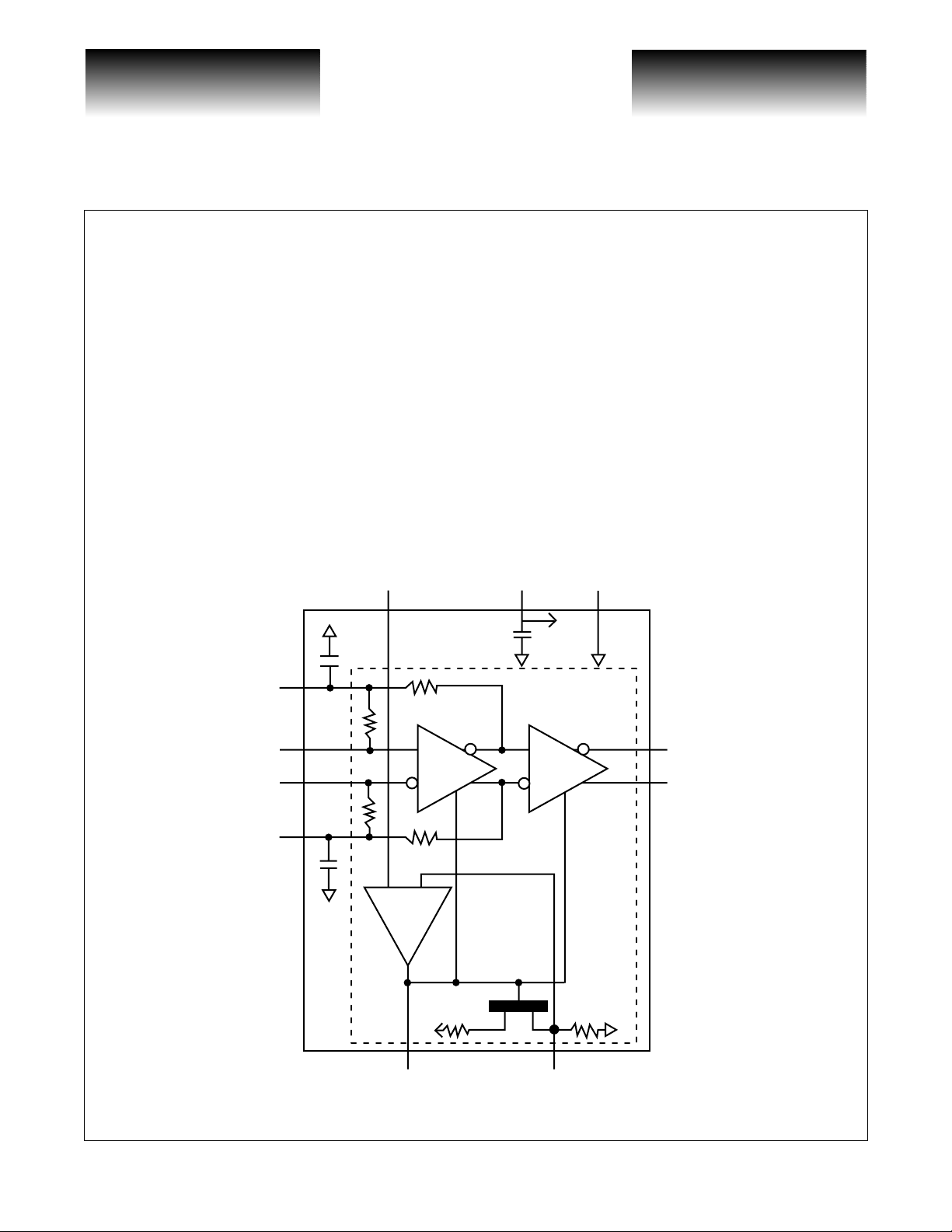
VSC7958 Block Diagram
VBR
VSS GND
VREF-
VIN-
VIN+
VREF+
50
50
Chip Boundary
A1 A2
+-
VBF VBS
VOUTVOUT+
G52184-0, Rev 3.0 Page 1
05/14/01
© VITESSE SEMICONDUCTOR CORPORATION • 741 Calle Plano • Camarillo, CA 93012
Tel: (800) VITESSE • FAX: (805) 987-5896 • Email: prodinfo@vitesse.com
Internet: www.vitesse.com
Page 2
VITESSE
SEMICONDUCTOR CORPORATION
2.5Gb/s High Speed Limiting Post Amplifier
Preliminary Data Sheet
for OC-48/SDH-16 Applications
T able 1: Electrical Specifications
All min and max values are tested at VSS = -4.5V and -5.5V, unless otherwise noted. All min and max values are guaranteed from
T
= 0°C to 85°C, unless otherwise noted.
CASE
Symbol Parameter Min Typ Max Units Conditions
(1)
VIN±
+) - (VIN-)
(V
IN
+) - (V
(V
REF
(V
+) - (V
OUT
V
OFFSET
PW% Output Pulse Width 90 100 110 %
, t
t
R
F
G Small Signal Gain 26 30 45 dB
(1)
f
MAX
(1)
f
MIN
(1)
S
11
(1)
S
22
I
SS
(1)
NF
(1)
V
NR
θ
JC
NOTE:(1) These values are not measured during production test. These values are results of engineering characterization.
Input Voltage Swing - - 800 mV
(1)
Input Voltage Swing - - 1600 mV
-) Input Offset Voltage Swing - 10 25 mV VIN = 0
REF
Single-ended source
p-p
Differential source
p-p
Differential Output Swing.
-) Output Voltage Swing 320 500 1200 mV
OUT
p-p
V
IN
Input peak-to -peak
Output DC Offset Voltage - -0.5 - V Measured to ground
Rise and Fall Time - 100 - ps
20%-80%, 25°C,
V
IN
V
IN
ended
Small Signal -3dB Bandwidth - 3 - GHz 25°C, VIN = 4mV
Low Frequency -3dB Cutoff - 30 - kHz 25°C, VIN = 4mV
Input Return Loss Reference to 50Ω - 15 - dB At 1. 5GHz
Output Return Loss Reference to 50Ω - 15 - dB At 1.5 GHz
Supply Current - 80 100 mA
Noise Figure - 15 - dB 8kHz to 18GHz
Total single-ended output
Input Referred Wide Band Noise - 170 - µV
noise voltage divided by
rms
small-signal gain. 8kHz to
18GHz
Thermal Resistance - 30 - °C/W Junction-to-case
= 8mV, Differential
= 50mV
= 4mV
VSC7958
single-
p-p
p-p
p-p
Page 2 G52184-0, Rev 3.0
© VITESSE SEMICONDUCTOR CORPORATION • 741 Ca l le Pl an o • Camarillo, CA 93012
Tel: (800) VITESSE • FAX: (805) 987-5896 • Email: prodinfo@vitesse.com
Internet: www.vitesse.com
05/14/01
Page 3
VITESSE
SEMICONDUCTOR CORPORATION
Preliminary Data Sheet
VSC7958
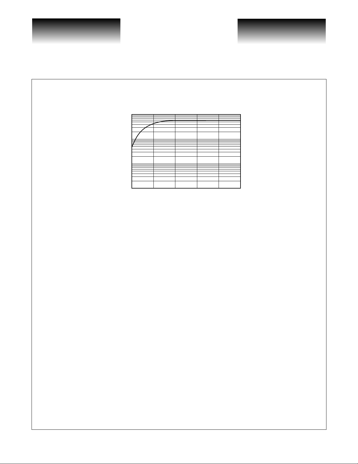
Figure 1: Typical Output Voltage vs. Input Voltage of Limiting Amplifier
1000
100
10
Single-Ended Output Voltage (mV)
Absolute Maximum Ratings
Output Voltage vs. Input Voltage
1
1
13
Single-Ended Input Voltage (mV)
(1)
(at TA = 25°C unless otherwise specified)
2.5Gb/s High Speed Limiting Post Amplifier
for OC-48/SDH-16 Applications
20 100 260 500
Power Supply Voltage (VSS) ...............................................................................................................-7V to -0.5V
Power Dissipation.............................................................................................................................................. 1W
All Pins............................................... ........ .........................................................................................V
SS
(VREF+) - (VIN+): ..........................................................................................................................................±2V
(VREF-) - (VIN-): ........................................................................................................................................... ±2V
Storage Temperature Range (T
)................................................................................................ -40°C to 125°C
STG
Operating Temperature Range ............................................................................................................0°C to 100°C
NOTE: (1) CAUTION: Stresses listed under “Absolute Maximum Ratings” may be applied to devices one at a time without caus-
ing permanent damage. Functionality at or above the values listed is not implied. Exposure to these values for extended
periods may affect device reliability.
to + .5V
Recommended Operating Conditions
Case Temperature Range (TC)..............................................................................................................0°C to 85°C
Negative Voltage Rail (V
Bit Rate = 2.488Gb/s NRZ and data pattern = 2
G52184-0, Rev 3.0 Page 3
05/14/01
).............................................................................................................-5.5V to -4.7V
SS
© VITESSE SEMICONDUCTOR CORPORATION • 741 Calle Plano • Camarillo, CA 93012
Tel: (800) VITESSE • FAX: (805) 987-5896 • Email: prodinfo@vitesse.com
23
-1 PRBS, unless otherwise specified.
Internet: www.vitesse.com
Page 4

VITESSE
SEMICONDUCTOR CORPORATION
2.5Gb/s High Speed Limiting Post Amplifier
for OC-48/SDH-16 Applications
Package Pin Descriptions
Figure 2: Pin Configuration
GND
GND
GND
1
VOUT+
VOUT-
GND
2
VSC7958
3
4
5678
GND
GND
(TOP VIEW)
.230
VBS
VSS
VBF
1315 1416
VBR
Preliminary Data Sheet
VSC7958
12
11
10
9
VREF+
.030
VIN+
VIN-
VREF-
.012
.366
.050
0.005
(SIDE VIEW)
*All values are typical in inches
Page 4 G52184-0, Rev 3.0
© VITESSE SEMICONDUCTOR CORPORATION • 741 Ca l le Pl an o • Camarillo, CA 93012
Tel: (800) VITESSE • FAX: (805) 987-5896 • Email: prodinfo@vitesse.com
Internet: www.vitesse.com
05/14/01
Page 5

VITESSE
SEMICONDUCTOR CORPORATION
Preliminary Data Sheet
VSC7958
Package Information
D1
D
A2
2.5Gb/s High Speed Limiting Post Amplifier
Figure 3: Package Dimensions
E1
A
e
for OC-48/SDH-16 Applications
E
Key Dimension Tolerance
A0.054REF
A1 0.003 ±0.003
A2 0.050 REF
D 0.366 ±0.010
D1 0.225 ±0.005
E 0.366 ±0.010
E1 0.225 ±0.005
L 0.020 ±0.005
e0.030REF
b0.012Typ.
θ 0-10
R 0.013 ±0.003
R1 0.013 ±0.003
Shoulder 0.020
All Dimensions in inches
R
— C — — C —
θ
L
G52184-0, Rev 3.0 Page 5
05/14/01
© VITESSE SEMICONDUCTOR CORPORATION • 741 Calle Plano • Camarillo, CA 93012
Sholder
b
R1
LEAD COPLANARITY
Tel: (800) VITESSE • FAX: (805) 987-5896 • Email: prodinfo@vitesse.com
Internet: www.vitesse.com
A1
Page 6

VITESSE
SEMICONDUCTOR CORPORATION
2.5Gb/s High Speed Limiting Post Amplifier
for OC-48/SDH-16 Applications
Die Information
Figure 4: Die Pad Information
1233µm
Pad 18
VREF_N
Pad19
VDD
Pad 20
VIN_N
Pad 21
VDD
Pad 22
VDD
Pad 17
VREFC_N
Pad 16
VBR
Pad 15
VSS_C
Pad 14
VSS
VSC7958
T op Vie w
1705
µm
Pad 13
VSS
Pad 12
VDD
Preliminary Data Sheet
VSC7958
Pad 11
VDD
Pad 10
VDD
Pad 9
EDGE_SENSE
Pad 8
VDD
Pad 7
VDD
Pad 15
Pad 6
GND
VOUT_N
Pad 5
VDD
Pad 4
VDD
Pad 23
VIN_P
Pad 24
VDD
Pad 25
VREF_P
Pad 26
VREFC_P
Pad 27
VBF
Pad 28
VBS
Maximum Total Die Size: 1233µm x 1705µm
Die Thickness: 305µm
Pad Size: 100µm x 100µm
Pad Passivation Opening: 90µm x 90µm
This device requires external components when used in die form.
Please contact your Vitesse sales representative for information.
Pad 29
VDD
Pad 30
VDD
Pad 31
VDD
Pad 3
VOUT_P
Pad 2
VDD
Pad 8
VDD
Page 6 G52184-0, Rev 3.0
© VITESSE SEMICONDUCTOR CORPORATION • 741 Ca l le Pl an o • Camarillo, CA 93012
Tel: (800) VITESSE • FAX: (805) 987-5896 • Email: prodinfo@vitesse.com
Internet: www.vitesse.com
05/14/01
Page 7

VITESSE
SEMICONDUCTOR CORPORATION
Preliminary Data Sheet
VSC7958
Table 2: Pin Identifications
Pin # Name Function
1, 4, 5, 6, 15 , 16,
and bottom heat
spreader
2 VOUT+ POSITIVE DATA OUTPUT
3 VOUT- NEGATIVE DATA OUTPUT
7 VSS NEGATIVE DC SUPPLY
8VBR
9VREF-
10 VIN- NEGATIVE DATA INPUT
11 VIN+ POSITIVE DATA INPUT
12 VREF+
13 VBF
14 VBS
GND
2.5Gb/s High Speed Limiting Post Amplifier
for OC-48/SDH-16 Applications
DEVICE GROUND
The package bottom heat spreader should be connected to ground for the optimum thermal
and electrical performance.
DEVICE REFERENCE VOLTAGE
This pin can either float or be set to an external -1.5V supply.
NEGATIVE DATA INPUT REFERENCE
This pin should be bypassed to ground with a 0.1µF cap and a 5Ω series resistor.
POSITIVE DATA INPUT R EFERENCE
This pin should be bypasSed to ground with a 0.1µF cap and a 5Ω series resistor.
INTERNAL TEST POINT
Do not connect.
INTERNAL TEST POINT
Do not connect.
Ordering Informatio n
The order number for this product is formed by a combination of the device number, and package style.
VSC7958
Device Type
VSC7958: 2.5Gb/s Limiting Amplifier
Notice
Vitesse Semiconductor Corporation (“Vitesse”) provides this document for informational purposes only. This document contains pre-production
information about Vitesse products in their con ce pt , development and/or testing phase . All i nformation in this document , inc lu d in g de scriptions of
features, functions, performan ce, technical specifications and availability, is subject to change wi th out notice at any ti me. Nothing contained in this
document shall be c ons trued as e xten ding an y w arran ty or pr omise , e xp ress or imp lied , th at a ny Vitesse produ ct wi ll b e av ail able as described or
will be suitable for or will accomp lis h any particular task.
Vitesse products are not intended for use in life support applia nc es, devices or systems. Use of a Vitesse product in such applications without written consent is prohibited.
G52184-0, Rev 3.0 Page 7
05/14/01
© VITESSE SEMICONDUCTOR CORPORATION • 741 Calle Plano • Camarillo, CA 93012
Tel: (800) VITESSE • FAX: (805) 987-5896 • Email: prodinfo@vitesse.com
Internet: www.vitesse.com
XX
Package Style
CC: (Metal Glass - Formed Leads)
X : (Bare Die)
Page 8

VITESSE
SEMICONDUCTOR CORPORATION
2.5Gb/s High Speed Limiting Post Amplifier
for OC-48/SDH-16 Applications
This page left intentionally blank.
Preliminary Data Sheet
VSC7958
Page 8 G52184-0, Rev 3.0
© VITESSE SEMICONDUCTOR CORPORATION • 741 Ca l le Pl an o • Camarillo, CA 93012
Tel: (800) VITESSE • FAX: (805) 987-5896 • Email: prodinfo@vitesse.com
Internet: www.vitesse.com
05/14/01
 Loading...