

Page 1
VITESSE
SEMICONDUCTOR CORPORATION
Preliminary Data Sheet
VSC7939
Laser Diode Driver with Automatic Power Control
SONET/SDH 3.125Gb/s
Features Applications
• Power Supply: 3.3V or 5V ±5%
• AC-Coupled to Laser Diode
• Programmable Modulation Current: 5mA to 60mA
• Programmable Bias Current: 1mA to 100mA
• Enable /Disable Control
• Typical Rise/Fall Times of 60ps
• Automatic Optical Average Power Control
• Supply Current of 33mA at 3.3V
• SONET/SDH at 622Mb/s, 1.244Gb/s,
2.488Gb/s, 3.125Gb/s
• Full-Speed Fibre Channel (1.062Gb/s)
General Description
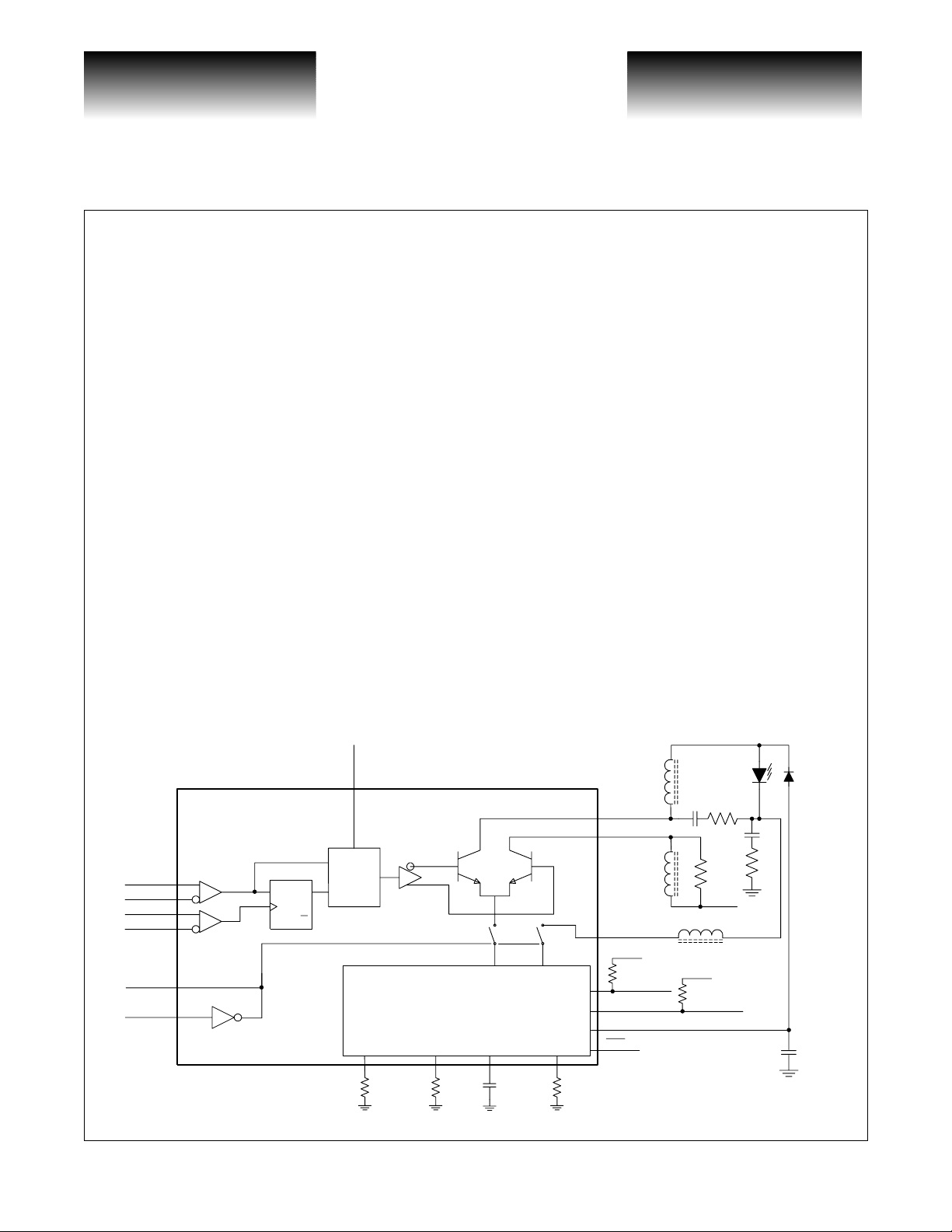
The VSC7939 is a single 3.3V or 5V supply l aser diode driv er special ly desig ned for S ONET/SDH appli cations up to 3.125Gb/s. External resistors set a wide range of bias and modulation currents for driving the laser.
Data and clock inputs accept differential PECL signals. The autom atic power control (APC) loop maintains a
constant average optical power over temperature and lifetime. The dominant pole of the APC loop can be controlled with an external capacitor. Other features include enable/disable control, short-circuit protection for the
modulation and bias inputs, short rise and fall times, programmable slow-start circuit to set laser turn-on delay,
and failure-monitor output to indicate when the APC loop is unable to maintain the average optical power. The
VSC7939 is available in die form or in a 32-pin TQFP package.
Block Diagram
V
P
L
C
D
P
L
V
CC
BIASMON
CC
C
F
R
F
V
CC
1nF
3.3V Operation
LATCH
IOUT+
IOUT-
MUX
DATA+
DATA-
CLK+
CLK-
ENABLE
DISABLE
G52350-0, Rev 3.2 Page 1
02/26/01
SET
D
Q
Q
CLR
APC
MODSET
© VITESSE SEMICONDUCTOR CORPORATION • 741 Calle Plano • Camarillo, CA 93012
Tel: (800) VITESSE • FAX: (805) 987-5896 • Email: prodinfo@vitesse.com
BIASMAX
Internet: www.vitesse.com
CAPC
APCSET
V
MODMON
MD
FAIL
BIAS
CC
Page 2
VITESSE
SEMICONDUCTOR CORPORATION
SONET/SDH 3.125Gb/s
Preliminary Data Sheet
Laser Diode Driver with Automatic Power Control
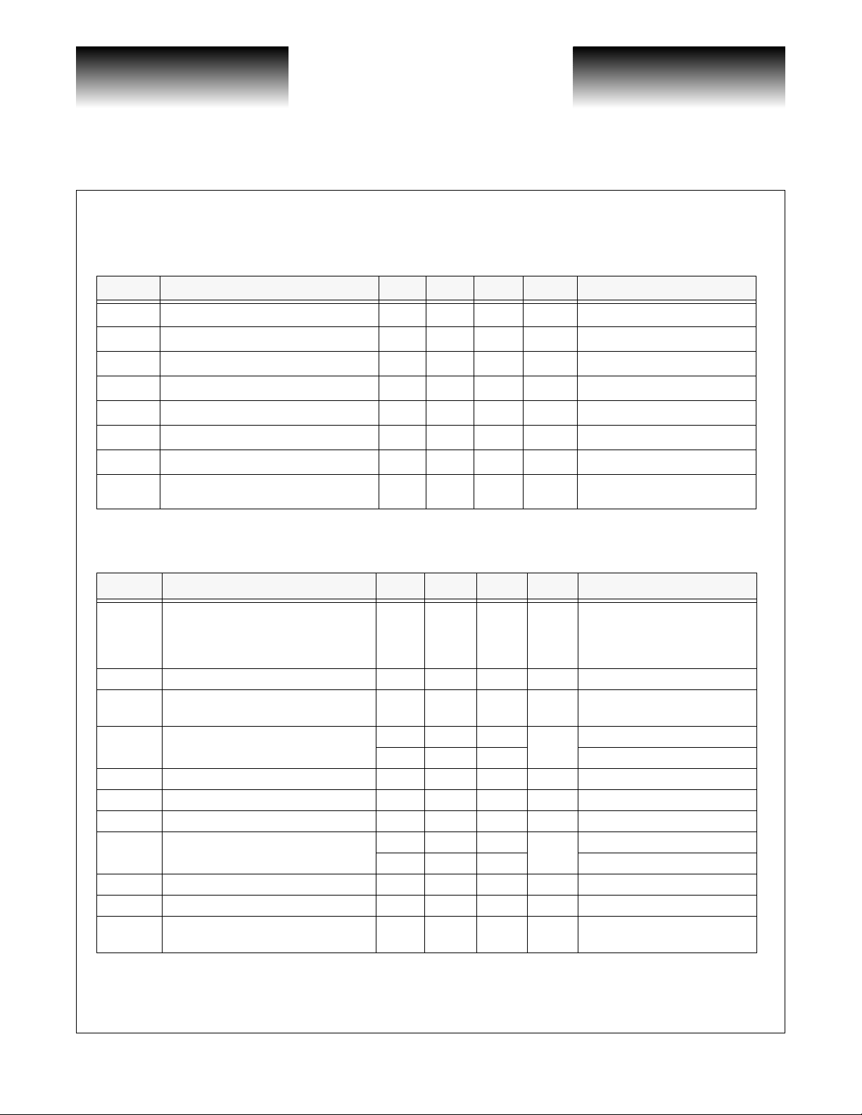
Electrical Characteristics
Table 1: AC Specifications
AC specifications are guaranteed by design an d characterization. Typical values are for 3.3V.
Symbol Parameter Min Typ Max Units Conditions
t
SU
t
H
t
R
t
F
PWD Pulse Width Distortion 10 50 ps See Notes 1, 2
CID
t
J
NOTES: (1) Measured with 622Mb/s 0-1 pattern , LATCH=high. (2) P WD = (wi der pulse - narrower pulse) / 2).
Input Latch Setup Time 100 ps LATCH=high
Input Latch Hold Time 100 ps LATCH=high
Enable/Start-up Delay 250 ns
Output Rise Time 60 80 ps 20% to 80%
Output Fall Time 60 80 ps 20% to 80%
Maximum Consecu tive Identical D igits 80 bits
MAX
Jitter Generation 7 20 ps
p-p
Jitter BW=12kHz to 20MHz,
0-1 pattern.
VSC7939
Table 2: DC Specifications
Symbol Parameter Min Typ Max Units Conditions
I
CC
I
BIAS
I
BIAS-OFF
S
BIAS
VR
MD
I
MD
I
MOD
I
MOD-OFF
R
Supply Current TBD 45 mA
Bias Current Range 1 100 mA Voltage at BIAS pin=(VCC-1.6)
Bias Off Current 100 µA
Bias Current Stability
Bias Current Absolute Accuracy ±15 % Refers to part-to-part variation
Monitor Diode Reverse Bias Voltage 1.5 V
Monitor Diode Reverse Current Range 18 1000 µA
Monitor Diode Bias Setpoint Stability
Monitor Diode Bias Absolute Accuracy -15 15 % Refers to part-to-part variation
Modulation Curren t Rang e 5 60 mA
Modulation Off Cu rr ent 200 µA
-480 -50 480
230
900 APC open loop. I
90 IMD=18µA
ppm/°C
ppm/°C
R
I
BIAS
V
ENABLE=low or
DISABLE=high
APC open loop. I
I
MD
ENABLE=low or
DISABLE=high
MODSET
BIASMAX
and I
=5V
CC
=1mA
=7.3kΩ
=4.8kΩ
MOD
(2)
(2)
excluded
(1)
BIAS
BIAS
(1)
=100mA
=1mA
Page 2 G52350-0, Rev 3.2
© VITESSE SEMICONDUCTOR CORPORATION • 741 Calle Plano • Camarillo, CA 93012
Tel: (800) VITESSE • FAX: (805) 987-5896 • Email: prodinfo@vitesse.com
Internet: www.vitesse.com
02/26/01
Page 3

VITESSE
SEMICONDUCTOR CORPORATION
Preliminary Data Sheet
VSC7939
Laser Diode Driver with Automatic Power Control
SONET/SDH 3.125Gb/s
Symbol Parameter Min Typ Max Units Conditions
Modulation Current Absolute Accuracy ±15 % See Note 2
Modulation Current Stability
A
BIAS
A
MOD
NOTES: (1) Both I
BIASMON to I
MODMON to I
tion does not change with temperature.
BIAS
and I
-480 -50 480
250 I
Gain 37 A/A I
BIAS
Gain 29 A/A I
MON
will turn off if any of the current set pins are grounded. (2) Assume s l ase r di ode t o monitor diode transfer func-
MOD
ppm/°C
I
=60mA
MOD
=5mA
MOD
BIAS/IBIASMON
MOD/IMODMON
Table 3: PECL and TTL/CMOS Inputs and Outputs Specifications
Symbol Parameter Min Typ Max Units Conditions
V
ID
V
ICM
I
IN
V
IH
V
IL
Differential Input Voltage 100 1600 mV
-
V
Common-Mode Input V oltage
Clock and Data Input Current -1 10 µA
TTL Input High Voltage
(ENABLE, LATCH)
TTL Input Low Voltage
(ENABLE, LATCH)
TTL Output High Voltage (FAIL
TTL Output Low Vo ltage (FAIL
)2.4
) 0.1 0.44 V Sinking 100µA
CC
1.49
2.0 V
VCC -
1.32
V
0.3
CC
-
VCC V
/4
ID
0.8 V
V
CC
V PECL-compatible
V Sourcin g 50µA
(DATA+)-(DATA-)
p-p
G52350-0, Rev 3.2 Page 3
02/26/01
© VITESSE SEMICONDUCTOR CORPORATION • 741 Calle Plano • Camarillo, CA 93012
Tel: (800) VITESSE • FAX: (805) 987-5896 • Email: prodinfo@vitesse.com
Internet: www.vitesse.com
Page 4

VITESSE
SEMICONDUCTOR CORPORATION
SONET/SDH 3.125Gb/s
Laser Diode Driver with Automatic Power Control
Absolute Maximum Ratings
Power Supply Voltage (VCC).............................................................................................................-0.5V to +7V
Current into BIAS.....................................................................................................................-20mA to +150mA
Current into OUT+, OUT-...............................................................................................................................TBD
Current into MD.............................................................................................................................-5mA to +5mA
Current into FAIL
Voltage at DATA+, DATA-, CLK+, CLK-, ENABLE, LATCH.........................................-0.5V to (V
Voltage at APCFILT, MODSET, BIASMAX, APCSET, MD, FAIL
Voltage at OUT+, OUT-..................................................................................................... -0.5V to (V
Voltage at BIAS..................................................................................................................-0.5V to (V
Continouous Power Dissipation (T
Operating Junction Temperature Range...................................................................................... -55°C to +150°C
Storage Temperature Range ........................................................................................................ -65 °C to +165°C
NOTE: (1) CAUTION: Stresses listed under “Absolute Maximum Ratings” may be applied to devices one at a time without caus-
ing permanent damage. Functionality at or above the values listed is not implied. Exposure to these values for extended
periods may affect device reliability.
......................................................................................................................... -10mA to 30mA
= +85°C, TQFP derate 20.8mW/°C above +85°C) .......................1350mW
A
(1)
.............................................-0.5V to +3.0V
Preliminary Data Sheet
VSC7939
CC
CC
CC
+ 0.5V)
+ 1.5V)
+ 0.5V)
Recommended Operating Conditions
Positive Voltage Rail (VCC).....................................................................................................+3.135V to +5.25V
Negative Voltage Rail (GND) ............................................................................................................................0V
Modulation Current (I
Ambient Temperature Range (T
NOTE: (1) VCC = 3.3V, I
MOD
BIAS
(1)
)
.......................................................................................................................30mA
).................................................................................................-40°C to +85°C
A
= 60mA.
Page 4 G52350-0, Rev 3.2
© VITESSE SEMICONDUCTOR CORPORATION • 741 Calle Plano • Camarillo, CA 93012
Tel: (800) VITESSE • FAX: (805) 987-5896 • Email: prodinfo@vitesse.com
Internet: www.vitesse.com
02/26/01
Page 5
VITESSE
SEMICONDUCTOR CORPORATION
Preliminary Data Sheet
VSC7939
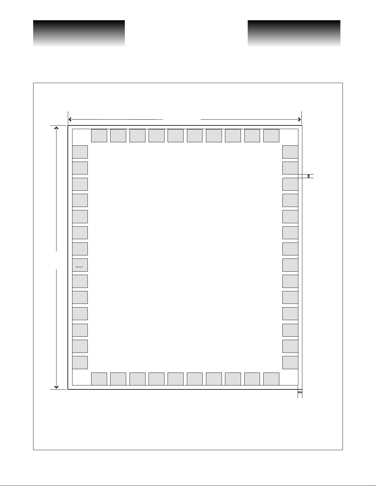
Bare Die Pad Descriptions
Pad 10
Pad 12
GND1
Pad 13
LATCH
Pad 14
ENABLE
Pad 15
DISABLE
Pad 16
GND1
Pad 17
BIASMON
Pad 11
VCC1
(Pin 7)
(Pin 8)
(Pin 9)
(Pin 10)
(Pin 11)
CLK-
Laser Diode Driver with Automatic Power Control
Figure 1: Pad Assignments
1773
µm (0.0698")
Pad 9
CLK+
Pad 8
VCC1
Pad 7
GND1
Pad 6
VCC1
Pad 5
DATA-
Pad 4
DATA+
SONET/SDH 3.125Gb/s
Pad 3
VCC1
(Pin 1)(Pin 2)(Pin 3)(Pin 4)(Pin 5)(Pin 6)
Pad 2
GND1
(Pin 32)
(Pin 31)
(Pin 30)
(Pin 29)
Pad 1
GND2
Pad 48
VCC2
Pad 47
BIASMAX
Pad 46
MODSET
Pad 45
GND2
Pad 44
APCSET
20
µm
(0.0008")
2233
µm
(0.0879")
Pad 18
(Pin 12)
MODMON
Pad 19
FAIL
Pad 20
GND4
Pad 21
PB_GND
Pad 22
APCFILT
Pad 23
GND4
Pad 24
VCC4
Pad 25
BIAS
(Pin 13)
(Pin 14)
(Pin 15)
(Pin 16)
(Pin 17)
Pad 26
PB_GND1
(Pin 18) (Pin 19) (Pin 20) (Pin 21) (Pin 22) (Pin 23) (Pin 24)
Pad 27
VCC4
Pad 28
DB_OUT+
Pad 29
OUT+
VSC7939
Pad 30
OUT-
Pad 31
DB_OUT-
Die Size: 1773µm x 2233µm (0.0698" x 0.0879")
Die Thickness: 625
µm (0.0246")
Pad Pitch: 115µm (0.0045")
Pad Size: 95µm x 95µm (0.0037" x 0.0037")
Pad to Pad Clearance: 20µm (0.0008
")
Pad Passivation Opening: 95µm x 95µm (0.0037" x 0.0037")
Scribe Size: 75µm (0.0030")
Pad 32
VCC4
Pad 33
GND4
Pad 34
GND3
(Pin 28)
(Pin 27)
(Pin 26)
(Pin 25)
Pad 35
MD
Pad 43
RESERVED
Pad 42
GND3
Pad 41
PB_GND
Pad 40
GND3
Pad 39
PB_GND
Pad 38
CAPC
Pad 37
VCC3
Pad 36
GND3
75
(0.0030")
µm
G52350-0, Rev 3.2 Page 5
02/26/01
© VITESSE SEMICONDUCTOR CORPORATION • 741 Calle Plano • Camarillo, CA 93012
Tel: (800) VITESSE • FAX: (805) 987-5896 • Email: prodinfo@vitesse.com
Internet: www.vitesse.com
Page 6
VITESSE
SEMICONDUCTOR CORPORATION
SONET/SDH 3.125Gb/s
Laser Diode Driver with Automatic Power Control
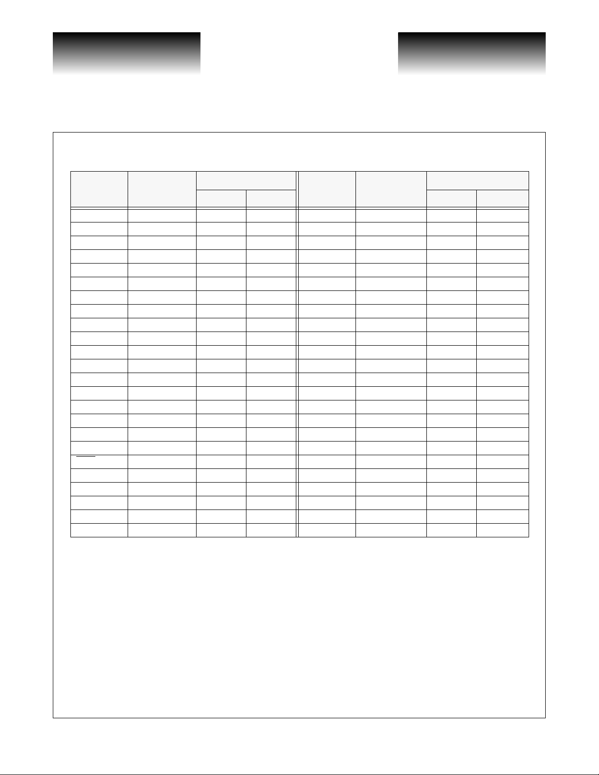
Table 4: Pad Coordinates
Signal
Name
GND2 1 1613.55 1863.475 BIAS 25 (Pin 17) 159.45 368.475
GND1 2 1414.525 2073.55 PB_GND 26 369.525 159.45
VCC1 3 (Pin 1) 1289.525 2073.55 VCC4 27 (Pin 18) 484.525 159.45
DATA+ 4 (Pin 2) 1174.525 2073.55 DB_OUT+ 28 599.525 159.45
DATA- 5 (Pin 3) 1059.525 2073.55 OUT+ 29 (Pin 19 ) 714.525 159.45
VCC1 6 (Pin 4) 944.525 2073.55 OUT– 30 (Pin 20) 829.525 159.45
GND1 7 829.525 2073.55 DB_OUT– 31 944.525 159.45
VCC1 8 714.525 2073.55 VCC4 32 (Pin 21) 1059.525 159.45
CLK+ 9 (Pin 5) 599.525 2073.55 GND4 33 (Pin 22) 1174.525 159.45
CLK- 10 (Pin 6) 484.525 2073.55 GND3 34 (Pin 23) 1289.525 159.45
VCC1 11 (Pin 7) 369.525 2073.55 MD 35 (Pin 24) 1404.525 159.45
GND1 12 159.45 1863.475 GND3 36 1613.55 368.475
LATCH 13 (Pin 8) 159.45 1748.475 VCC3 37 (Pin 25) 1613.55 483.475
ENABLE 14 (Pin 9) 159.45 1633.475 CAPC 38 (Pin 26 ) 1613.55 598.475
DISABLE 15 (Pin 10) 159.45 1518.475 PB_GND 39 1613.55 713 .475
GND 16 159.45 1403.4 GND3 40 (Pin 27) 1613.55 828.475
BIASMON 17 ( Pin 11) 159.45 1288.475 PB_GND 41 1613.55 943.475
MODMON 18 (Pin 12) 159.45 1058.475 GND3 42 1613.55 1058.475
FAIL
GND4 20 159.45 943.475 APCSET 44 (Pin 29) 1613.55 1288.475
PB_GND 21 159.45 828.475 GND2 45 1613.55 1403.475
APCFILT 22 (Pin 14) 159.45 713.475 MODSET 46 (Pin 30) 1613.55 1518.475
GND4 23 (Pin 15) 159.45 598.475 BIASMAX 47 (Pin 31) 1613.55 1633.475
VCC4 24 (Pin 16) 159.45 483.475 VCC2 48 (Pin 32) 1613.55 1748.475
Pad
No.
19 (Pin 13) 159.45 1058.475 RESERVED 43 (Pin 28) 1613.55 1173.475
Coordinates (µm)
X Y X Y
Signal
Name
Preliminary Data Sheet
VSC7939
Pad
No.
Coordinates (µm)
Page 6 G52350-0, Rev 3.2
© VITESSE SEMICONDUCTOR CORPORATION • 741 Calle Plano • Camarillo, CA 93012
Tel: (800) VITESSE • FAX: (805) 987-5896 • Email: prodinfo@vitesse.com
Internet: www.vitesse.com
02/26/01
Page 7

VITESSE
SEMICONDUCTOR CORPORATION
Preliminary Data Sheet
VSC7939
Package Pin Description
VCC
DATA+
DATA-
VCC
CLK-
CLK+
VCC
LATCH
SONET/SDH 3.125Gb/s
Laser Diode Driver with Automatic Power Control
Figure 2: Pin Diagram
VCC
BIASMAX
MODSET
APCSET
RESERVED
GND
CAPC
VCC
32
31
30
29
28
27
26
25
1
2
3
4
5
6
7
8
VSC7939
24
23
22
21
20
19
18
17
MD
GND
GND
VCC
OUTOUT+
VCC
BIAS
9
10
11
12
13
14
15
16
FAIL
ENABLE
DISABLE
BIASMON
MODMON
G52350-0, Rev 3.2 Page 7
02/26/01
© VITESSE SEMICONDUCTOR CORPORATION • 741 Calle Plano • Camarillo, CA 93012
Tel: (800) VITESSE • FAX: (805) 987-5896 • Email: prodinfo@vitesse.com
Internet: www.vitesse.com
APCFILT
GND
VCC
Page 8

VITESSE
SEMICONDUCTOR CORPORATION
SONET/SDH 3.125Gb/s
Preliminary Data Sheet
Laser Diode Driver with Automatic Power Control
Table 5: Pin Identifications
Pin Name Pin Number Description
GND 15, 22, 23, 27 Ground
V
CC
DATA+ 2 Positive Data Input (PECL)
DATA- 3 Negative Data Input (PECL)
CLK+ 5 Positive Clock Input (PECL). Connect to V
CLK- 6 Negative Clock Input (PECL) . Leave unconnect ed if LATCH function is not used.
LATCH 8 Latch Input (TTL/CMOS). Connect to VCC for data retiming and GND for direct data.
ENABLE 9
DISABLE 10
BIASMON 11 Bias Current Monitor. Sink current source that is proportional to the laser bias current.
MODMON 12
FAIL
APCFILT 14 No effect on device operation..
BIAS 17 Laser Bias Current Output
OUT+ 19 Positive Modulation-Current Output. I
OUT- 20 Negative Modulation-Current Output. I
MD 24
CAPC 26 Capacitor to GND sets dominan t pole of the APC feedback loop.
RESERVED 28 Do not connect.
APCSET 29
MODSET 30 Connect resistor to GND to set desired modulation current.
BIASMAX 31
1, 4, 7, 16,
18, 21, 25, 32
13 Output (TTL/CMOS). When low indicates APC failure.
Power Suppl y
Enable Input (TTL/CMOS). If used, connect DISABLE to GND. Connect to VCC for
normal operation and GND to disable laser bias and modulation currents.
Disable Input (TTL/CMOS). If used, leave ENABLE pin floating. Connect to GND for
normal operation and V
Modulation Current Monitor. Sink current source that is proportional to the laser
modulation current.
Monitor Diode Input. Connect to monitor photodiode anode. Connect capacitor to GND to
filter high-speed AC monitor photocurrent.
Resistor to GND sets desired average optical power. If APC is not used, connect 100kΩ
resistor to GND.
Connect resistor to GND to set maximum bias current. The APC function can subtract from
this value, but cannot add to it.
to disable laser bias and modulation currents.
CC
MOD
MOD
if LATCH function is not used.
CC
flows when input data is high.
flows when input data is low.
VSC7939
Page 8 G52350-0, Rev 3.2
© VITESSE SEMICONDUCTOR CORPORATION • 741 Calle Plano • Camarillo, CA 93012
Tel: (800) VITESSE • FAX: (805) 987-5896 • Email: prodinfo@vitesse.com
Internet: www.vitesse.com
02/26/01
Page 9

VITESSE
SEMICONDUCTOR CORPORATION
Preliminary Data Sheet
VSC7939
Laser Diode Driver with Automatic Power Control
SONET/SDH 3.125Gb/s
Detailed Description
The VSC7939 is a high-speed l aser dri ver with Automatic Power Con trol. The device is desig ned to operate
up to 3.125Gb/s with a 3.3V or 5V supply. The data and clock inputs support PECL inputs as well as other
inputs that meet the common-mode voltage and differential voltage swing specif ications. The differential pair
output stage is capab le of sinking up to 60mA from the l aser with typical rise and fall times of 60ps. This output
may be DC-coupled for 5V operation. To allow for larger output swings during 3.3V operation, the VSC7939
was designed to be AC-coupled to the laser cathode with a pull-up inductor for DC-biasing. This configuration
will isolate laser forward voltage from the output circuitry and will allow the output at OUT+ to s wing above
and below the supply voltage V
supply current, and fast ri se and fall times. Th e VSC7938 is another Vitesse laser drivers with simi lar feat ures in
a 48-pin TQFP package. The VSC7938 does not have monitoring for modulation and bias currents. The
VSC7940 is a modified version of the VSC7939 capable of 100mA output currents.
Automatic Power Control
To ensure constant average optical power, the VSC7939 utilizes an Automatic Power Control loop. A photodiode mounted in the laser packa ge pr ov ide s optica l f eed back t o comp ensat e f or chang e s in average l aser ou tput power due to ch anges tha t affect laser performan ce such a s temper ature and laser life time. Th e laser bia s
current is adjusted by the APC loop according to the reference current set at APCSET by an external resistor.
An external capacitor at CAPC controls the time constant for the APC feedback loop. The recommended value
for CAPC is 0.1
guarantees stability. Because the APC loop noise is internally filtered, APCFIL T is not internally connected and
does not need to be connected to any external components. The device’s performance will not be affected if a
capacitor is connected to APCFILT. If the APC loop cannot adjust the bias current to track the desired monitor
current, FAIL
The device may be operated with or without APC. To utilize APC, a capacitor must be connected at CAPC
(0.1
µF) and a resistor must be connected at APCSET to set the average optical power. For open-loop operation
(no APC), a 10 0k
loop operation. In both mo des of o peratio n, resist ors to ground sho uld be p laced at BIASMAX and MODSET to
set the bias and modulation currents.
µF. This value reduces pattern-dependent jitter associated with the APC feedback loop and
is set low.
Ω resistor should be connected between APCSET and GND. CAPC has no effect on open-
. The key features of the VSC7939 are Automatic Power Control, low power
CC
Data Retiming
The VSC7939 provides inpu ts for differential PECL cl ock signals for data ret iming to minim ize jitter at
high speeds. To incorporate this function, LATCH shou ld be connected to V
CLK+ should be connected to V
GND.
Short-Circuit Protection
If BIASMAX or MODSET are shorted to ground, the output mo dulation and bias currents will be turned
off.
G52350-0, Rev 3.2 Page 9
02/26/01
© VITESSE SEMICONDUCTOR CORPORATION • 741 Calle Plano • Camarillo, CA 93012
Tel: (800) VITESSE • FAX: (805) 987-5896 • Email: prodinfo@vitesse.com
, CLK- should be left unconnected, and LATCH should be connected to
CC
Internet: www.vitesse.com
. If this function is unused,
CC
Page 10

VITESSE
SEMICONDUCTOR CORPORATION
SONET/SDH 3.125Gb/s
Laser Diode Driver with Automatic Power Control
Modulation and Bias Current Monitors
Preliminary Data Sheet
VSC7939
The VSC7939 provides monitoring of the modulation and bias currents vias BIASMON and MODMON.
These pins sink a current proportiona l to the actual modu lation and bias curren ts. MODMON sinks approximately 1/28th of the amount of modulation current and BIASMON sink approximately 1/35th of the amount of
the bias current. These pins should be tied through a pull-up resistor to V
that the voltage at MODMON is greater than V
- 1.0V and the voltage at BIASMON is greater than VCC -
CC
. The resistors must be chosen such
CC
1.6V.
Enable/Disable
Two pins are provided to a llow either EN ABLE or DISABLE contr ol. If ENABLE is used, co nnect DISABLE to ground. Is DISABLE is used, leave ENABLE floating. Both modulation and bias currents are turned
off when ENABLE is low or DISABLE is high. Typically, ENABLE or DISABLE responds within approximately 250ns.
Controlling the Modulation Current
The output modulation current may be determined from the following equation where P
peak optical power, P
is the average power, r
AVE
I
MOD
= P
is the extinction ratio, and η is the laser slope efficiency:
e
/ η= 2 * P
p-p
* (re-1) / (re+1) / η
AVE
is the peak-to-
p-p
A resistor at MODSET controls the output bias current. Graphs of I
MODSET
vs. R
in Typical Operat-
MODSET
ing Characteristics for both 3.3V and 5V operation describe the relationship between the resistor at MODSET
and the output modulation current at 25
°C. After determining the desired outpu t modulatio n current, use the
graph to determine the appropriate resistor value at MODSET.
Controlling the Bias Current
A resistor at BIASMAX should be used to control the output bias current. Graphs of I
BIASMAX
vs. R
BIASMAX
in Typical Operating Characteristics for both 3.3V and 5V operation describe the relationship between the
resistor at BIASMAX and the output bias current at 25
°C. If the APC is not used, the appropriate resistor value
at BIASMAX is determined by first selecting the desired output bias current, and then using the graph to determine the appropriate resistor value at BIASMAX. When using APC, BIASMAX sets the maximum allowed
bias current. After determining the maximum end-of-life bias current at 85
I
BIASMAX
Controlling the APC Loop
vs. R
BIASMAX
To select the resistor at APCSET, use the graph of IMD vs. R
in Typical Operating Characteristics to select the appropriate resistor value.
APCSET
The graph relates the desired monitor current to the appropriate resistance value at APCSET. I
late from the desired optical average power, P
, and the laser-to-monitor transfer, ρ
AVE,
°C for the laser, refer to the graph of
in Typical Operating Characteristics.
may be calcu-
MD
, for a specific laser
MON
using the following equa tion:
I
MD
= P
AVE
* ρ
MON
Page 10 G52350-0, Rev 3.2
© VITESSE SEMICONDUCTOR CORPORATION • 741 Calle Plano • Camarillo, CA 93012
Tel: (800) VITESSE • FAX: (805) 987-5896 • Email: prodinfo@vitesse.com
Internet: www.vitesse.com
02/26/01
Page 11

VITESSE
SEMICONDUCTOR CORPORATION
Preliminary Data Sheet
VSC7939
Laser Diode Interface
Laser Diode Driver with Automatic Power Control
SONET/SDH 3.125Gb/s
An RC shunt network should be placed at the laser outpu t interface. Th e sum of the re sistor placed at the
output and the laser diode resistance should be 25
Ω resistor should be placed in series with the laser. For optimal performance, a bypass capacitor should be
20
Ω. For exam ple, if t he lase r diode ha s a resis tance of 5Ω, a
placed close to the laser anode.
A “snubber network” consisting of a capacitor C
and resistor RF should be placed at the laser output to
F
minimize reflections from the laser (see Block Diagram). Suggested values for these components are 80
2pF, respectively, however, these values should be adjusted until an optical output waveform is obtained.
Reducing Pattern-Dependent Jitter
Three design values significantly affect pattern-dependent jitter; the capacitor at CAPC, the pull-up inductor at the output (L
value for the capacitor at CAPC is 0.1
), and the AC-coupling c apaci t or at t he out put (CD). As previously stated, the recommended
P
µF. This results in a 10kHz loop bandwidth which makes the pattern-
dependent jitter from the APC loop negligible.
For 2.5Gb/s data rates, the recommended value for C
nated by L
. The variation in the peak vo ltage should be less that 12% of the average voltage over the maximum
P
is 0.056µF. The time constant at the output is domi-
D
consecutive identical digit (CID) period. The following equation approximates this time constant for a CID
period, t, of 100UI = 40ns:
τ
= -t / ln(1-12%) = 7.8t = LP / 25Ω
LP
Ω and
Therefore, the inductor LP should be a 7.8µH SMD ferrite bead inductor for this case.
Input/Output Considerations
Although the VSC7939 is PECL-compatible, this is not required to drive the device. The inputs must only
meet the common-mode voltage and differential voltage swing specifications.
Power Consumption
The following equation provides the device supply current (IS) in terms of quiescent current (IQ), modulation current (I
), and bias current (I
MOD
):
BIAS
I
= IQ + 0.47 * I
S
+ 0.15 * I
MOD
BIAS
For 3.3V operation, IQ is 15mA. For 5V operation, IQ is 20mA.
This equation may be used to determine the estimated power dissipation:
= VCC * I
P
DIS
S
For example, if the device were operated at 3.3V with a 30mA mod ulation current and a 10mA bias current ,
the supply current would be:
= 15mA + 0.47 * 30mA + 0.15 * 10mA = 31
I
S
This corresponds to a power dissipation of 3.3V * 31mA = 102mW.
G52350-0, Rev 3.2 Page 11
02/26/01
© VITESSE SEMICONDUCTOR CORPORATION • 741 Calle Plano • Camarillo, CA 93012
Tel: (800) VITESSE • FAX: (805) 987-5896 • Email: prodinfo@vitesse.com
Internet: www.vitesse.com
Page 12

VITESSE
SEMICONDUCTOR CORPORATION
SONET/SDH 3.125Gb/s
Laser Diode Driver with Automatic Power Control
Typical Operating Characteristics
I
MODSET
vs. R
MODSET
T=25°C VCC = 3.3V
Preliminary Data Sheet
VSC7939
I
MODSET
vs. R
MODSET
T=25°C VCC = 5V
I
BIASMAX
vs. R
T=25°C, VCC = 3.3V
BIASMAX
I
BIASMAX
vs. R
T=25°C, VCC = 5V
BIASMAX
Page 12 G52350-0, Rev 3.2
© VITESSE SEMICONDUCTOR CORPORATION • 741 Calle Plano • Camarillo, CA 93012
Tel: (800) VITESSE • FAX: (805) 987-5896 • Email: prodinfo@vitesse.com
Internet: www.vitesse.com
02/26/01
Page 13

VITESSE
SEMICONDUCTOR CORPORATION
Preliminary Data Sheet
VSC7939
IMD vs. R
T=25°C, V
APCSET
CC
,
= 3.3V
SONET/SDH 3.125Gb/s
Laser Diode Driver with Automatic Power Control
IMD vs. R
T=25°C, V
APCSET
= 5V
CC
,
Rise and Fall Times
T=85°C, V=3.3V
Monte Carlo Si mulation of I
CC
G52350-0, Rev 3.2 Page 13
02/26/01
© VITESSE SEMICONDUCTOR CORPORATION • 741 Calle Plano • Camarillo, CA 93012
Tel: (800) VITESSE • FAX: (805) 987-5896 • Email: prodinfo@vitesse.com
Internet: www.vitesse.com
Page 14

VITESSE
SEMICONDUCTOR CORPORATION
SONET/SDH 3.125Gb/s
Preliminary Data Sheet
Laser Diode Driver with Automatic Power Control
Applications Information
The following is a typical design example for the VSC7939 assuming 3.3V operation with APC.
Select a Laser
The Table 7 provides specifications for a typical communication-grade laser capable of operating at
2.5Gb/s.
Table 6: Typical Laser Characteristics
Symbol Parameter Value Units
λ W avelength 1310 nm
P
AVE
I
th
ρ
MON
η Laser Slope Efficiency 0.4 mW/mA
T
C
Select Resistor for APCSET
The monitor diode current is estimated by IMD = P
vs. R
APCSET
Average Opti cal Output Power 6 mW
Threshold Current 6 mA
Laser to Monitor Transfer 0.04 mA/mW
Operating Temperature Range -40 to +85 °C
AVE
* ρ
= 6mW * 0.04mA/mW = 0.24mA. The IMD
MON
in Typical Operating Characteristics shows the resistor at APCSET should be 5kΩ.
VSC7939
Select Resistor for MODSET
T o ensure some minimum extinction ratio over temperature and lifetime, assume an optimal extinction ratio
of 20 (13dB) at 25
I
MOD
The graph of I
should be 8.5k
Select Resistor for BIASMAX
°C. The modulation current may be calculated from the following equation:
= P
/ η= 2 * P
p-p
MODSET
vs. R
* (re-1) / (re+1) / η = 2 * 6mA * (20-1) / (20 + 1) / 0.4 = 27.1mA
AVE
MODSET
in Typical Operating Characteristics shows the resistor for MODSET
Ω.
The maximum threshold current at +85°C and end of life must be determined. A graph of a typical laser’s
versus TC reveals a maximum threshold current of 30mA at 85°C. Therefore, the maxim um bias can be
I
th
approximated by:
vs. R
= I
BIASMAX
I
BIASMAX
The graph of I
should be 5k
Select Resistors for MODMON and BIASMON
BIASMAX
Ω.
TH-MAX
+ I
/ 2 = 30mA + 27.1mA / 2 = 43.6mA
MOD
in T ypi cal Operating Characteristics shows the resistor for BIASMAX
Assuming the modulation and bias currents never exceed 120mA, the following equations provide values
for the resistor at MODMON, RMODMON, and the resistor at BIASMON, RBIASMON:
R
MODMON
= 1V * 28 / 120mA = 233Ω
R
BIASMON
Page 14 G52350-0, Rev 3.2
© VITESSE SEMICONDUCTOR CORPORATION • 741 Calle Plano • Camarillo, CA 93012
Tel: (800) VITESSE • FAX: (805) 987-5896 • Email: prodinfo@vitesse.com
= 1.6V * 35 / 120mA = 467Ω
Internet: www.vitesse.com
02/26/01
Page 15

VITESSE
SEMICONDUCTOR CORPORATION
Preliminary Data Sheet
VSC7939
Standard values for these values are R
MODMON would indicate a modulation current of:
I
MOD
Wire Bonding
For best performance, gold ball-bonding techniques are recommended. Wedge bonding is not recommended. For best performance and to minimize inductance keep wire bond lengths short.
MODMON
= (5.2V - 4.8V) * 28 / 232mA = 48mA
Laser Diode Driver with Automatic Power Control
= 232Ω and R
BIASMON
SONET/SDH 3.125Gb/s
= 464Ω. A voltage of 4.8V at
PCB Layout Guidelines
Use high frequency PCB layout techniques with solid ground planes to minimize crosstalk and EMI. Keep
high speed traces as short as possible for signal integrity. The output traces to the laser diode must be short to
minimize inductance. Short output traces will provide best performance.
G52350-0, Rev 3.2 Page 15
02/26/01
© VITESSE SEMICONDUCTOR CORPORATION • 741 Calle Plano • Camarillo, CA 93012
Tel: (800) VITESSE • FAX: (805) 987-5896 • Email: prodinfo@vitesse.com
Internet: www.vitesse.com
Page 16

VITESSE
SEMICONDUCTOR CORPORATION
SONET/SDH 3.125Gb/s
Laser Diode Driver with Automatic Power Control
Package Information - 32 Pin TQFP
Preliminary Data Sheet
VSC7939
1. All dimensioning and tolerancing conform to ANSI Y14.5-1982
2. Controlling dimension: millimeter
3. This outline conforms to JEDEC Publication 95 Registration MS-026
Page 16 G52350-0, Rev 3.2
© VITESSE SEMICONDUCTOR CORPORATION • 741 Calle Plano • Camarillo, CA 93012
Tel: (800) VITESSE • FAX: (805) 987-5896 • Email: prodinfo@vitesse.com
Internet: www.vitesse.com
02/26/01
Page 17

VITESSE
SEMICONDUCTOR CORPORATION
Preliminary Data Sheet
VSC7939
Ordering Informatio n
The order number for this product is formed by a combination of the device type and package type.
Device Type
SONET/SDH 3.125Gb/s
Laser Diode Driver with Automatic Power Control
SONET/SDH 3.125Gb/s
Laser Diode Driver with Automatic Power Control
VSC7939
xx
Package
RP: 32-Pin TQFP
W: Dice Waffle Pack
Notice
Vitesse Semiconductor Corporation (“Vitesse”) provides this document for informational purposes only. This document contains pre-production information
about Vitesse products in their co ncept , devel opmen t and/or te stin g phas e. All inf ormat ion in th is docu ment, inclu ding des cript ions of f eature s, functio ns,
performance, technical specifications and availability, is subject t o ch an g e without notice at any time. Nothing c ontained in this document shall be construed
as extending any war ranty or p romi se, e xpress or impl ied, that a ny Vitesse prod uct wi ll be a vail able a s de scrib ed or wi ll be suitable for or will accomplish
any particular task.
Vitesse products are not intended for use in life support appliances, devices or systems. Use of a Vitesse product in such applications without written consent
is prohibited.
G52350-0, Rev 3.2 Page 17
02/26/01
© VITESSE SEMICONDUCTOR CORPORATION • 741 Calle Plano • Camarillo, CA 93012
Tel: (800) VITESSE • FAX: (805) 987-5896 • Email: prodinfo@vitesse.com
Internet: www.vitesse.com
Page 18

VITESSE
SEMICONDUCTOR CORPORATION
SONET/SDH 3.125Gb/s
Laser Diode Driver with Automatic Power Control
Preliminary Data Sheet
VSC7939
Page 18 G52350-0, Rev 3.2
© VITESSE SEMICONDUCTOR CORPORATION • 741 Calle Plano • Camarillo, CA 93012
Tel: (800) VITESSE • FAX: (805) 987-5896 • Email: prodinfo@vitesse.com
Internet: www.vitesse.com
02/26/01
 Loading...