

Page 1
Preliminary Data Sheet
VITESSE
SEMICONDUCTOR CORPORATION
VSC7927
SONET/SDH 2.5Gb/s Laser Diode Driver
Features
• Rise Times of Less Than 100ps
• High Speed Operation
(Up to 2.5 Gb/s NRZ Data)
• Differential or Single-Ended Inputs
• Single Supply
• ECL-Compatible Clock and Data Inputs
• Direct Access to Modulation and Bias FETs
• Data Density Monito rs
• On-Chip Reclocking Register
• On-Chip Mux for Clocked or Non-clocked Applications
• On-Chip 50
Ω Input Termination: Clock and Data
General Description
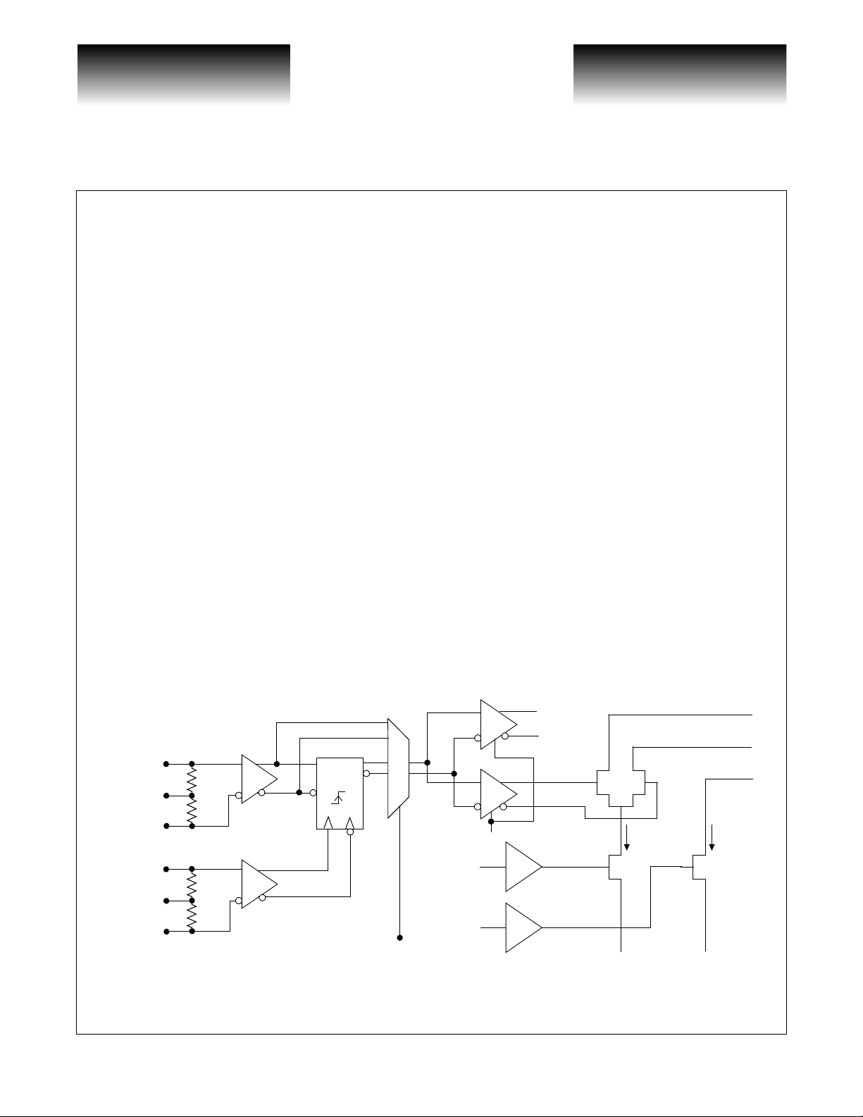
The VSC7927 is a single 5V supply, 2.5 Gb/s laser diode driver with direct access to the laser modulation
and bias FETs. Laser bias and modulation currents are set by external components allowing precision monitoring and setting of the current levels. Data density outputs are provided to allow the user to adjust the laser bias
in high unbalanced data applications. Clock and data inputs are differentially terminated to 50
Ω.
Applications
• SDH/SONET @ 622Mb/s, 1.244Gb/s, 2.488Gb/s
• Full Speed Fibre Channel (1.062Gb/s)
VSC7927 Block Diagram
DIN
DINTERM*
NDIN
CLK
CLKTERM*
NCLK
*Terminated to Off-chip Capacitor
**On Die Components
50 Ω
50 Ω
50 Ω
50 Ω
**
**
**
**
DQ
M
U
X
SEL
VIP
VIB
DCC
MK
NMK
MIP
I
MOD
MIB
IOUT
NIOUT
IBIAS
I
BIAS
G52201-0, Rev 3.0 Page 1
04/05/01
© VITESSE SEMICONDUCTOR CORPORATION • 741 Calle Plano • Camarillo, CA 93012
Tel: (800) VITESSE • FAX: (805) 987-5896 • Email: prodinfo@vitesse.com
Internet: www.vitesse.com
Page 2
VITESSE
SEMICONDUCTOR CORPORATION
Preliminary Data Sheet
SONET/SDH 2.5Gb/s Laser Diode Driver
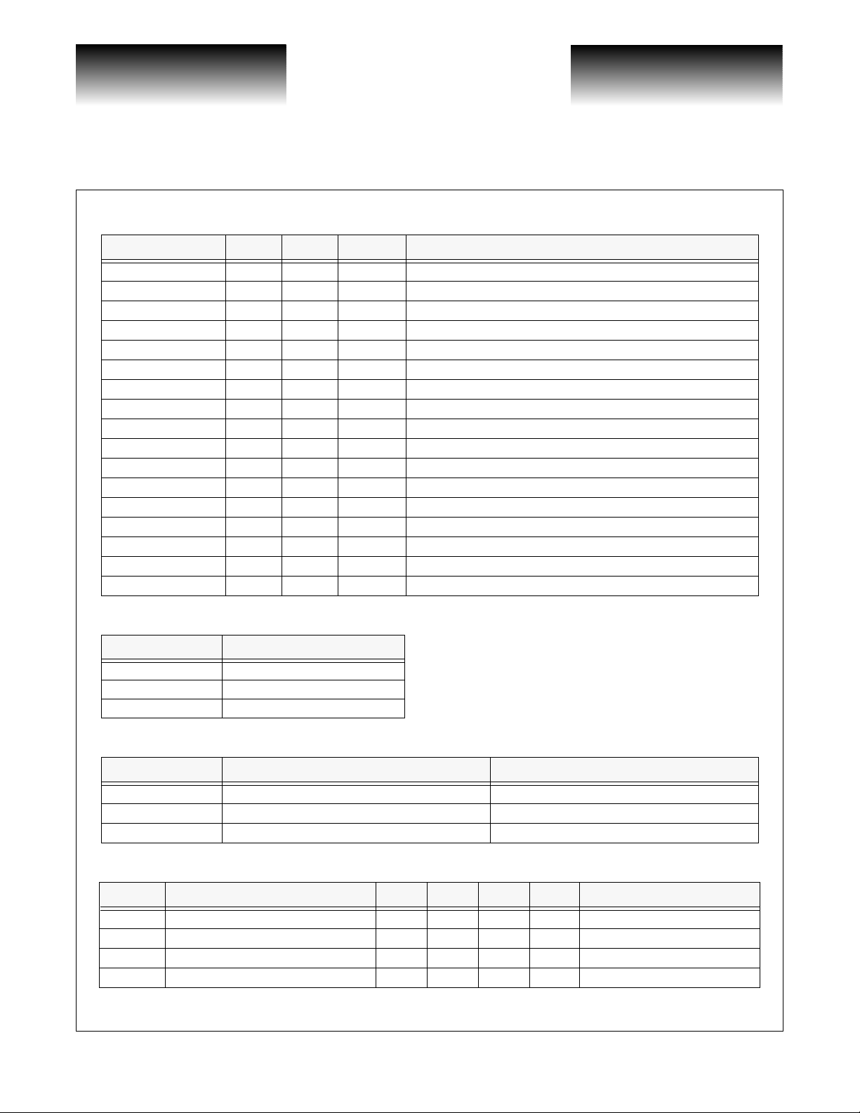
Table 1: Signal Pin Reference
Signal Type Level # Pins Description
DIN, NDIN In ECL 2 Data Input and Data Reference, On-chip 50Ω Termination
MK, NMK Out ECL 2 Data Density Differential Outputs
NIOUT Out
IOUT Out — 1 Laser Modulation Current Output (to Laser Cathode)
VSS Pwr Pwr 2 Negative Voltage Rail
GND Pwr Pwr 5 Positive Voltage Rail
VIP In DC 1 Modulation Gate Node
MIP In DC 1 Modulatio n Sou r ce Node
VIB I n DC 1 Bias Gate Node
MIB In DC 1 Bias Source Node
IBIAS Out DC 1 Laser Bias Output (To Laser Cathode)
CLK, NCLK In ECL 2 Clock Input and Clock Reference, On-chip 50Ω Termination
DINTERM In DC 1 Data Reference
CLKTERM In DC 1 Clock Reference
DCC In DC 1 Duty Cycle Control, Leave Floating
SEL In DC 1 Clk/Non-clk Data Select
T otal Pin s
—— 24
— 1 Laser Modulation Current Output (Complementary)
VSC7927
Table 2: Mux Select Logic Table
SEL Mode Select
V
SS
GND Non-clocked Data In
N/C Non-clocked Data In
Clocked Data In
Table 3: Absolute Maximum Ratings
Symbol Rating Limit
V
SS
T
J
T
STG
Negative Power Supply Voltage VCC to -6.0V
Maximum Junction Temperature -55°C to + 125°C
Storage Temperature -65°C to +150°C
Table 4: Recommended Operating Conditions
Symbol Parameter Min Typ Max Units Conditions
GND Positive Voltage Rail — 0 — V
VSS Negative Voltage Rail -5.5 -5.2 -4.9 V
T
Cl
T
J
NOTES: (1) Lower limit of specification is ambient temperature and upper limit is case temperature. (2) See section “Calculation of the
Operational Temperature
Junction Temperature ——125 °C
Maximum Case Temperature” for detailed maximum temperature calculations.
(1)
-40 — 85
(2)
°C Power dissipation = 1.3W
Page 2 G52201-0, Rev 3.0
© VITESSE SEMICONDUCTOR CORPORATION • 741 Ca l le Pl an o • Camarillo, CA 93012
Tel: (800) VITESSE • FAX: (805) 987-5896 • Email: prodinfo@vitesse.com
Internet: www.vitesse.com
04/05/01/01
Page 3
Preliminary Data Sheet
VITESSE
SEMICONDUCTOR CORPORATION
VSC7927
SONET/SDH 2.5Gb/s Laser Diode Driver
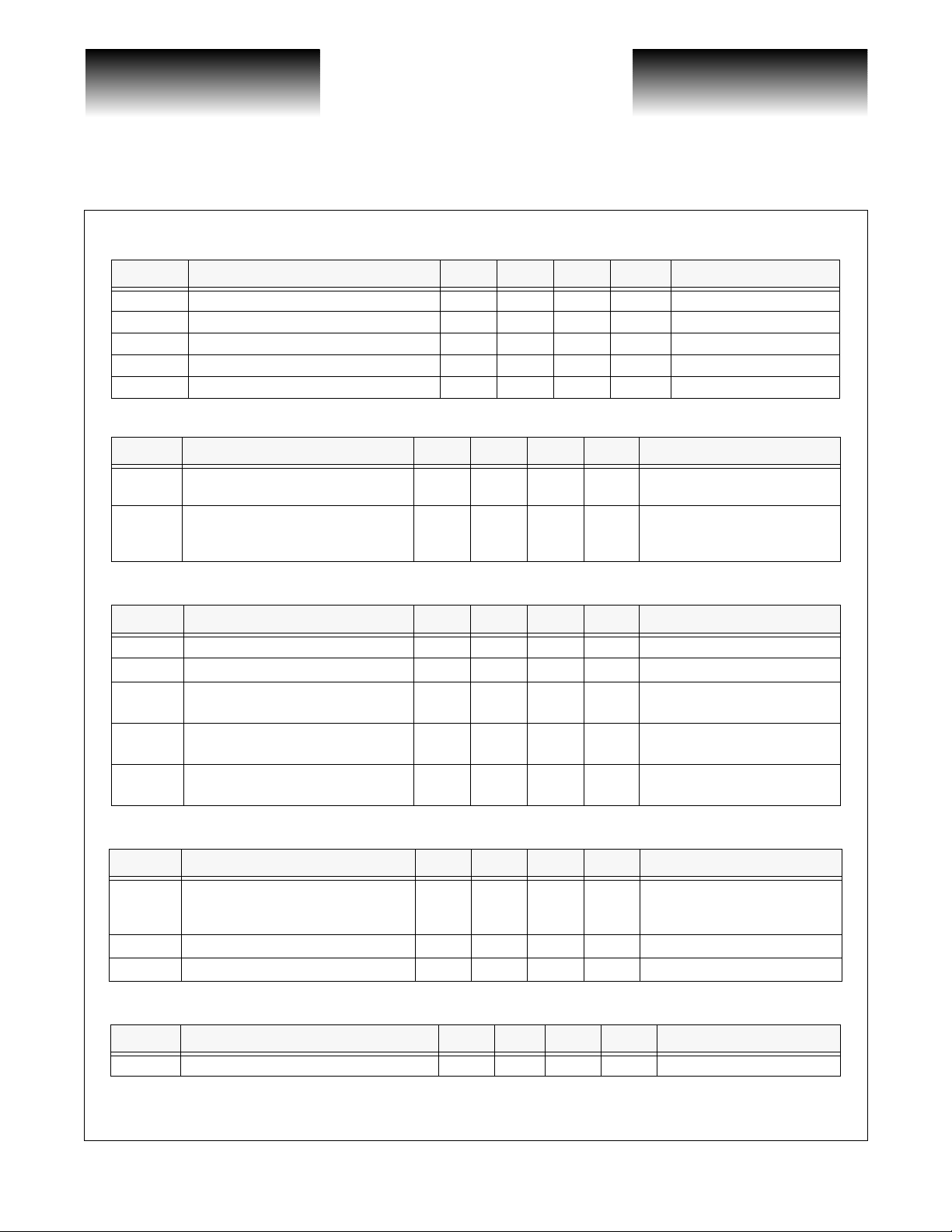
Table 5: High Speed Inputs and ECL Outputs
Symbol Parameter Min Typ Max Units Conditions
V
IN
V
CM
V
OH
V
OL
V
IN
Single-ended Input Voltage Swing 300 — 1500 mVp-p V
Differential Input Common Mode Range -2.3 — -1.3 V VSS = -5.2V
ECL Output High Vol tag e -1200 ——mV 50Ω to -2.0V
ECL Output Low Voltage ——-1600 mV 50Ω to -2.0V
On-Chip Terminations 35 — 65 Ω
CM
Table 6: Power Diss ipat ion
Symbol Parameter Min Typ Max Units Conditions
= -5.5V, I
V
I
P
VSS
D
Power Supply Current (VSS) ——120 mA
Total Power Dissipation ——700 mW
SS
0mA, MK/NMK open circuit
V
= -5.5V, I
SS
0mA, R
LOAD
MK/NMK terminated 50Ω to -2V
T able 7: Laser Driver DC Electrical Specifications
Symbol Parameter Min Typ Max Units Conditions
I
BIAS
I
MOD
V
V
V
IB
IP
OCM
Programmable Laser Bias Current 2 — 100 mA —
Programmable Modulation Current 2 — 100 mA
V
+
Laser Bias Control Voltage ——
Laser Modulation Control Voltage ——
Output Voltage Compliance —
GND -
3V
SS
2.1
V
+
SS
2.1
— VV
—
VI
VI
BIAS
MOD
SS
= 50mA
= 60mA
= -5.2V
= -2.0V
= I
MOD
BIAS
= I
MOD
= 25Ω to GND,
BIAS
=
=
T able 8: Laser Driver AC Electrical Specifications
Symbol Parameter Min Typ Max Units Conditions
25Ω load, 20%-80%,
tR, t
t
SU
t
H
F
Output Rise and Fall Times ——100 ps
Data to Clock Setup Time — 50 90 ps
Hold Time 20 50 — ps
20mA < I
= 60mA
I
BIAS
—
—
MOD
< 60mA,
Table 9: Package Thermal Specifications
Symbol Parameter Min Typ Max Units Conditions
θ
JCC
G52201-0, Rev 3.0 Page 3
04/05/01
Thermal Resistance from Junction-to-Case — 25 — °C/W Ceramic Package
© VITESSE SEMICONDUCTOR CORPORATION • 741 Calle Plano • Camarillo, CA 93012
Tel: (800) VITESSE • FAX: (805) 987-5896 • Email: prodinfo@vitesse.com
Internet: www.vitesse.com
Page 4

VITESSE
SEMICONDUCTOR CORPORATION
Preliminary Data Sheet
SONET/SDH 2.5Gb/s Laser Diode Driver
VSC7927
Calculation of the Maximum Case Temperature
The VSC7927 is designed to operate with a maximum junction temperature of 125°C. The rise from the
case to junction is determined by the power dissip ation of the dev ice. The power dissipation is determine d by
the V
current plus the operating I
SS
MOD
and I
BIAS
currents.
The power of the chip is determined by the following formula:
P
= (-VSS * ISS) + ((V
D
IOUT – VSS
) * I
MOD
For example with:
V
SS
I
MOD
I
BIAS
V
IBIAS
V
IOUT
P
D
P
D
=-5.2V
=40mA
=20mA
=-2.0V
=-2.0V
= (-5.2 * 150mA) + ((5.2 - 2.0) * 40mA) + ((5.2-- 2.0) * 20mA)
= 780mW + 128mW + 64mW = 972mW
) + ((V
IBIAS – VSS
) * I
BIAS
)
θ
The thermal rise from junction-to-case is
* PD. For the ceramic package, θ
JC
mal rise is:
25°C/W * 972W = 24.3°C
The maximum case temperature is:
125°C – 24.3°C = 100.7°C
The absolute maximum power dissipation of the device is at:
V
I
MOD
I
BIAS
V
IBIAS
V
IOUT
P
D
P
D
SS
=-5.5V
=60mA
=50mA
=0V
=0V
= (5.5 * 150mA) + (5.5 * 60mA) + (5.5mA * 50mA)
= 1.43W
This will net a maximum junction to case thermal rise of: 1.43W * 25°C/W = 35.8°C
This situation will allow maximum case temperature of: 35.8°C – 58°C = 89.2°C
= 25°C/W. Thus the ther-
JCP
Page 4 G52201-0, Rev 3.0
© VITESSE SEMICONDUCTOR CORPORATION • 741 Ca l le Pl an o • Camarillo, CA 93012
Tel: (800) VITESSE • FAX: (805) 987-5896 • Email: prodinfo@vitesse.com
Internet: www.vitesse.com
04/05/01/01
Page 5

Preliminary Data Sheet
VITESSE
SEMICONDUCTOR CORPORATION
VSC7927
DIN
(CLK)
DINTERM
(CLKTERM)
NDIN
(NCLK)
SONET/SDH 2.5Gb/s Laser Diode Driver
Figure 1: On-chip Data and Clock Input Configuration
GND GND
X
50
*
4.0K
*
X
*
50
6.4K
*
X
*On-chip
Components
DINTERM to -2.0V for Differential ECL Inputs
Figure 2: Single-Ended Operation
DATA BUFFER
(CLOCK BUFFER)
VSSVSS
DA T A
SOURCE
CLOCK
SOURCE
0.1µf
0.1µf
GND
GND
0.1µf
0.1µf
0.1µf
0.1µf
7927
DIN
DINTERM
NDIN
GND
CLK
CLKTERM
NCLK
GND
G52201-0, Rev 3.0 Page 5
04/05/01
© VITESSE SEMICONDUCTOR CORPORATION • 741 Calle Plano • Camarillo, CA 93012
Tel: (800) VITESSE • FAX: (805) 987-5896 • Email: prodinfo@vitesse.com
Internet: www.vitesse.com
Page 6

VITESSE
SEMICONDUCTOR CORPORATION
Preliminary Data Sheet
SONET/SDH 2.5Gb/s Laser Diode Driver
Figure 3: Single-Ended AC-Coupled
SOURCE
0.1µf
GND
Figure 4: Differential AC-Coupled
0.1µf
SOURCE
0.1µf
0.1µf
DINTERM
(CLKTERM)
NDIN
(NCLK)
0.1µf
GND
DIN
(CLK)
X
X
X
DIN
(CLK)
X
DINTERM
(CLKTERM)
X
VSC7927
GND
50
50
50
4.0K
-2.0V
6.4K
VSS
GND
4.0K
-2.0V
SOURCE
0.1µf
NDIN
(NCLK)
X
GND
Figure 5: Differential DC-Coupled
DIN
(CLK)
X
DINTERM
(CLKTERM)
X
NDIN
(NCLK)
X
-2.0V
50
50
50
6.4K
VSS
GND
4.0K
-2.0V
6.4K
VSS
Page 6 G52201-0, Rev 3.0
© VITESSE SEMICONDUCTOR CORPORATION • 741 Ca l le Pl an o • Camarillo, CA 93012
Tel: (800) VITESSE • FAX: (805) 987-5896 • Email: prodinfo@vitesse.com
Internet: www.vitesse.com
04/05/01/01
Page 7

Preliminary Data Sheet
VITESSE
SEMICONDUCTOR CORPORATION
VSC7927
SONET/SDH 2.5Gb/s Laser Diode Driver
Figure 6: Control Signals VIP and VIB
I (MIB)
30 mA
VIB
VSS + 1.5 Volts (Typical)
Typical Bias Current v.s. Bias Voltage
I (MIP)
60 mA
VIP
VSS + 1.5 Volts (Typical)
VIP
X
Typical Modulation Current v.s. Modulation Voltage
Figure 7: Simplified Output Structure
NIOUT IOUT
XXX
I
MOD
OUTPUT
DIFF
PAIR
IBIAS
X
I
BIAS
X
MIP
MIB
X
VIB
G52201-0, Rev 3.0 Page 7
04/05/01
© VITESSE SEMICONDUCTOR CORPORATION • 741 Calle Plano • Camarillo, CA 93012
Tel: (800) VITESSE • FAX: (805) 987-5896 • Email: prodinfo@vitesse.com
Internet: www.vitesse.com
Page 8

VITESSE
SEMICONDUCTOR CORPORATION
Preliminary Data Sheet
SONET/SDH 2.5Gb/s Laser Diode Driver
Figure 8: Pad Assignments for VSC7927 Die
50µm
PAD 34 PAD 33 PAD 32 PAD 31 PAD 30 PAD 29 PAD 28 PAD 27 PAD 26
120
DCC VSS VSS VSS VSS VIP MIP MIP MIB
120µm
150µm
30µm
PAD 1
N/C
PAD 2
NDIN
PAD 3
DIN
PAD 4
DINT
PAD 5
CLOCKT
PAD 6
CLOCK
1720µm
1620µm
PAD 25
VIB
PAD 24
GND
PAD 23
IOUT
PAD 22
IOUT
PAD 21
GND
PAD 20
GND
50µm
VSC7927
50µm
1620µm
1720µm
PAD 7
NCLOCK
PAD 8
N/C
SEL GND GND GND GND GND GND NMARK MARK
PAD 9 PAD 10 PAD 11 PAD 12 PAD 13 PAD 14 PAD 15 PAD 16 PAD 17
Die Size: 1620µm x 1620µm
Actual Die Size: 1720µmx1720µm (after the die are cut up)
Pad Size: 120µm x 120µm
Pad Pitch: 150µm
Space
Between Pads: 30µm
PAD 19
NIOUT
PAD 18
IBIAS
50µm
Page 8 G52201-0, Rev 3.0
© VITESSE SEMICONDUCTOR CORPORATION • 741 Ca l le Pl an o • Camarillo, CA 93012
Tel: (800) VITESSE • FAX: (805) 987-5896 • Email: prodinfo@vitesse.com
Internet: www.vitesse.com
04/05/01/01
Page 9

Preliminary Data Sheet
VITESSE
SEMICONDUCTOR CORPORATION
VSC7927
Pin Diagram for 24-Pin Ceramic Package
DCC
VSS
NDIN
DIN
DINTERM
CLKTERM
24 23 22 21 20 19
1
2
3
4
VSS
SONET/SDH 2.5Gb/s Laser Diode Driver
VIP
MIP
MIB
18
17
16
15
VIB
GND
IOUT
GND
CLK
NCLK
MK
14
13
MK
5
6
78910
SEL
GND
GND
Note: Package lid and bottom he at s pre ad e r are ele c tr ic ally
connected to GND within the package.
11 12
GND
NIOUT
IBIAS
G52201-0, Rev 3.0 Page 9
04/05/01
© VITESSE SEMICONDUCTOR CORPORATION • 741 Calle Plano • Camarillo, CA 93012
Tel: (800) VITESSE • FAX: (805) 987-5896 • Email: prodinfo@vitesse.com
Internet: www.vitesse.com
Page 10

VITESSE
SEMICONDUCTOR CORPORATION
Preliminary Data Sheet
SONET/SDH 2.5Gb/s Laser Diode Driver
Package Information - 24 Pin Ceramic Package (Formed Leads)
Top View
A
24 23 22 21 20 19
INDEX
E
1
2
3
A
4
5
18
17
16
15
14
Key mm In
A 9.5 0.374
B 7.7 0.303
C 2.0 0.079
D1.27 0.050
E0.30 0.012
F 1.7 0.067
G 0.6 0.024
H11.5 0.453
I 0.125 0.005
J8.51 0.335
VSC7927
6
78910
D
11 12
13
Side View
B
F
I
G
J
H
NOTES:
Drawing not to scale.
Package #: 101-000-0 Issue #:1
C
Page 10 G52201-0, Rev 3.0
© VITESSE SEMICONDUCTOR CORPORATION • 741 Ca l le Pl an o • Camarillo, CA 93012
Tel: (800) VITESSE • FAX: (805) 987-5896 • Email: prodinfo@vitesse.com
Internet: www.vitesse.com
04/05/01/01
Page 11

Preliminary Data Sheet
VITESSE
SEMICONDUCTOR CORPORATION
VSC7927
SONET/SDH 2.5Gb/s Laser Diode Driver
Package Information - 24 Pin Ceramic Package (Straight Leads)
Top View
A
24 23 22 21 20 19
INDEX
E
1
2
3
A
4
5
18
17
16
15
14
Key mm In
A 9.5 0.374
B 7.7 0.303
C 5.8 .230
D1.27 0.050
E0.30 0.012
F 1.7 0.067
G 0.6 0.024
H9.53 0.375
I 0.125 0.005
J8.51 0.335
6
78910
D
11 12
13
Side View
B
I
C
HC
NOTES:
Drawing not to scale.
F
G
G52201-0, Rev 3.0 Page 11
04/05/01
© VITESSE SEMICONDUCTOR CORPORATION • 741 Calle Plano • Camarillo, CA 93012
Tel: (800) VITESSE • FAX: (805) 987-5896 • Email: prodinfo@vitesse.com
Internet: www.vitesse.com
Page 12

VITESSE
SEMICONDUCTOR CORPORATION
Preliminary Data Sheet
SONET/SDH 2.5Gb/s Laser Diode Driver
Ordering Informatio n
The order number for this product is formed by a combination of the device number, and package style.
VSC7927
Device Type
VSC7927: 2.5Gb/s Laser Diode Driver
*Optional Reversed Formed Leads: Package leads have the same profile and dimensions,
but heat spreader is away from board. Please contact the factory for additional information.
VSC7927
XX
Package Style
KF: (Ceramic - Straight Leads)
KFL: (Ceramic- Formed Leads)
KFRL: (Ceramic - Reversed Formed Leads}*
X : (Bare Die)
Notice
Vitesse Semiconductor Corporation (“Vitesse”) provides this document for informational purposes only. This document contains pre-production
information about Vitesse products in their con ce pt , development and/or testing phase. All information in this do cument, including descriptions of
features, functions, performan ce, technical specifications and availability, is subject to change wi th out notice at any ti me. Nothing contained in this
document shall be c ons trued as e xten ding an y w arran ty or pr omise , e xp ress or imp lied , th at a ny Vitesse produ ct wi ll b e av ail able as described or
will be suitable for or will accomp lis h any particular task.
Vitesse products are not intended for use in life support applia nc es, devices or systems. Use of a Vitesse product in such applications without written consent is prohibited.
Page 12 G52201-0, Rev 3.0
© VITESSE SEMICONDUCTOR CORPORATION • 741 Ca l le Pl an o • Camarillo, CA 93012
Tel: (800) VITESSE • FAX: (805) 987-5896 • Email: prodinfo@vitesse.com
Internet: www.vitesse.com
04/05/01/01
 Loading...