

Page 1
VITESSE
SEMICONDUCTOR CORPORATION
Preliminary Data Sheet
VSC7926
SDH/SONET 2.5Gb/s Laser Diode Driver
G52188-0, Rev 3.0 Page 1
04/05/01
© VITESSE SEMICONDUCTOR CORPORATION • 741 Calle Plano • Camarillo, CA 93012
Tel: (800) VITESSE • FAX: (805) 987-5896 • Email: prodinfo@vitesse.com
Internet: www.vitesse.com
Features
General Description
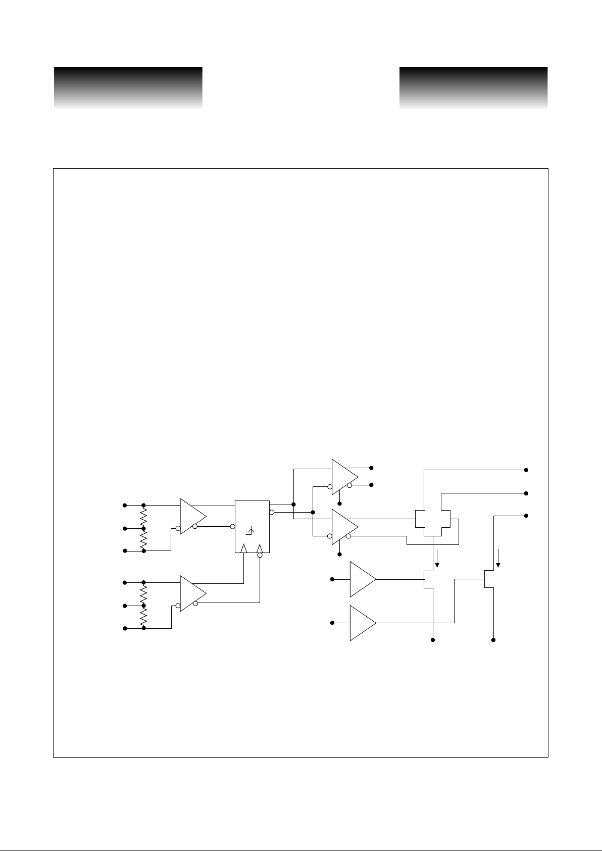
The VSC7926 is a single 5V supply, 2.5Gb/s laser diode driver with direct acce ss to the laser modulation
and bias FETs. Laser bias and modulation currents are set by external components allowing precision monitoring and setting of the current levels. Data density outputs are provided to allow the user to adjust the laser bias
in high unbalanced data applications. Clock and data inputs are differentially terminated to 50
Ω.
Applications
• SDH/SONET @ 622Mb/s, 1.244Gb/s, 2.488Gb/s
• Full Speed Fibre Channel (1.062Gb/s)
VSC7926 Block Diagram
• Rise Times of Less Than 100ps
• High-Speed Operation
(Up to 2.5Gb/s NRZ Data)
• Differential Inputs
• Single Supply
• Direct Access to Modulation and Bias FETs
• Data Density Monitors
• On-Chip Reclocking Register
DIN
DINTERM*
50 Ω
MK
NMK
IBIAS
NIOUT
IOUT
MIP
VIP
VIB
MIB
DQ
DCC
**
**On Die Components
I
MOD
I
BIAS
50 Ω
**
NDIN
CLK
50 Ω
**
50 Ω
**
NCLK
CLKTERM*
*Terminated to Off-chip Capacitor
DCC
Page 2
VITESSE
SEMICONDUCTOR CORPORATION
Preliminary Data Sheet
VSC7926
SDH/SONET 2.5Gbits /sec
Laser Diode Driver
Page 2 G52188-0, Rev 3.0
04/05/01
© VITESSE SEMICONDUCTOR CORPORATION • 741 Ca ll e Pl an o • Camarillo, CA 93012
Tel: (800) VITESSE • FAX: (805) 987-5896 • Email: prodinfo@vitesse.com
Internet: www.vitesse.com
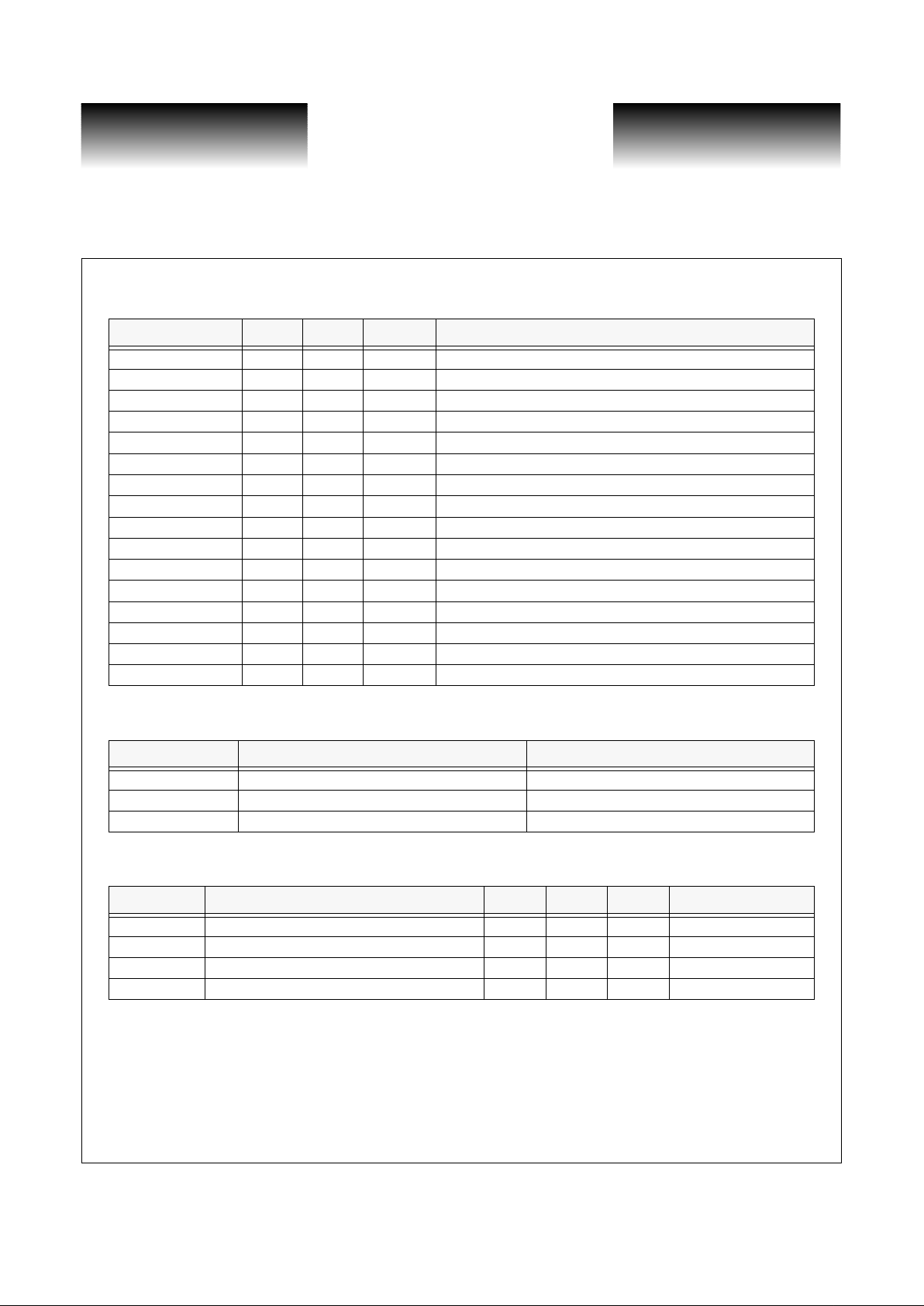
Table 1: Signal Pin Reference
Table 2: Absolute Maximum Ratings
Table 3: High Speed Inputs and ECL Outputs
Signal Type Level # Pins Description
DIN, NDIN In 2 Data Input and Data Reference
DINTERM Ref DC 1 Data Termination
CLKTERM Ref DC 1 Clock Termination
MK, NMK Out ECL 2 Data Density Differential Outputs
NIOUT Out 1 Laser Modulation Current Output (Complementary)
IOUT Out 1 Laser Modulation Current Output (To Laser Cathode)
VSS Pwr Pwr 3 Negative Voltage Rail
GND Pwr Pwr 5 Positive Voltage Rail
VIP In DC 1 Modulation Gate Node
MIP In DC 1 Modulation Source Node
VIB In DC 1 Bias Gate Node
MIB In DC 1 Bias Sour ce Node
IBIAS Out DC 1 Laser Bias Output (To Laser Cathode)
CLK, NCLK In 2 Clock Input and Clock Reference
DCC In DC 1 Duty Cycle Control, Leave Floating
T otal Pin s 24
Symbol Rating Limit
V
SS
Negative Power Supply Voltage VCC to -6.0V
T
j
Maximum Junction Temperature -55°C to + 125°C
T
stg
Storage Temperature -65°C to +150°C
Symbol Parameter Min Max Units Conditions
V
IN
Differential Input Voltage Swing 500 1000 mV
V
CM
Differential Input Common Mode Range -2.3 -1.3 V VSS = -5.2V
V
OH
ECL Output High Voltage -1200 mV 50Ω to -2.0V
V
OL
ECL Output Low Voltage -1600 mV 50Ω to -2.0V
Page 3
VITESSE
SEMICONDUCTOR CORPORATION
Preliminary Data Sheet
VSC7926
SDH/SONET 2.5Gb/s Laser Diode Driver
G52188-0, Rev 3.0 Page 3
04/05/01
© VITESSE SEMICONDUCTOR CORPORATION • 741 Calle Plano • Camarillo, CA 93012
Tel: (800) VITESSE • FAX: (805) 987-5896 • Email: prodinfo@vitesse.com
Internet: www.vitesse.com
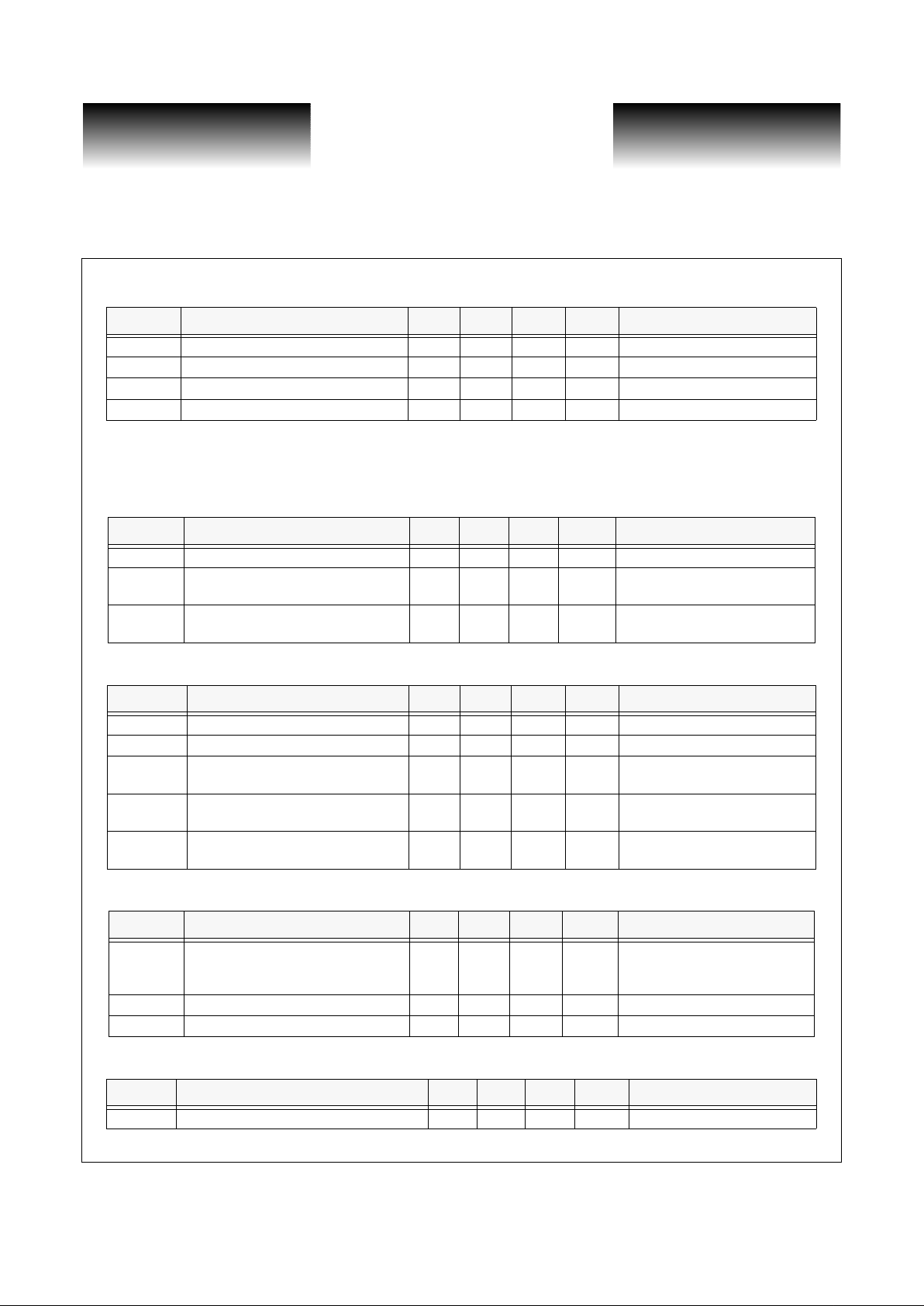
Table 4: Recommended Operating Conditions
NOTES: (1) Lower limit of specification is ambient temperature and upper limit is case temperature. (2) See “Calculation of the
Maximum Case Temperature” section in this data sheet for detailed maximum temperature calculations.
Table 5: Power Dissip atio n
Table 6: Laser Driver DC Electrical Specifications
Table 7: Laser Driver AC Electrical Specifications
Table 8: Package Thermal Specifications
Symbol Parameter Min Typ Max Units Conditions
GND Positive Voltage Rail - 0 - V
VSS Negative Voltage Rail -5.5 -5.2 -4.9 V
Tc
l
Operational Temperature
(1)
-40 - 85
(2)
°C Power dissipation = 1.25W
T
J
Junction Temperature - - 125 °C
Symbol Parameter Min Typ Max Units Conditions
I
VSS
Power Supply Current (VSS) - - 220 mA VSS = -5.5, I
MOD
= I
BIAS
= 0mA
P
D
T otal Po wer Dissipatio n - - 1210 mW
V
SS
= -5.5, I
MOD
= I
BIAS
= 0mA,
R
LOAD
= 25Ω to GND
P
DMAX
Maximum Power Dissipation - - 1815 mW
V
SS
= -5.5, I
MOD
= 60mA,
I
BIAS
= 50mA, I
OUT
= 0V
Symbol Parameter Min Typ Max Units Conditions
I
BIAS
Programmable Laser Bias Current 2 - 50 mA
I
MOD
Programmable Modulation Current 2 - 60 mA
V
IB
Laser Bias Control Voltage - -
V
SS
+
2.1
VI
BIAS
= 50mA
V
IP
Laser Modulation Control Voltage - -
V
SS
+
2.1
VI
MOD
= 60mA
V
OCM
Output Voltage Compliance
GND
-2.5V
--VV
SS
= -5.2V
Symbol Parameter Min Typ Max Units Conditions
tR t
F
Output Rise and Fall Times - - 100 ps
25Ω load, 20%-80%,
15mA < I
MOD
< 60 mA,
I
BIAS
= 40mA
t
SU
Setup Data to Clock Setup Time - 50 - ps
t
H
Hold Time - 50 - ps
Symbol Parameter Min Typ Max Units Conditions
θ
JCC
Thermal Resistance from Junction-to-Case - 25 - °C/W Ceramic Package
Page 4

VITESSE
SEMICONDUCTOR CORPORATION
Preliminary Data Sheet
VSC7926
SDH/SONET 2.5Gbits /sec
Laser Diode Driver
Page 4 G52188-0, Rev 3.0
04/05/01
© VITESSE SEMICONDUCTOR CORPORATION • 741 Ca ll e Pl an o • Camarillo, CA 93012
Tel: (800) VITESSE • FAX: (805) 987-5896 • Email: prodinfo@vitesse.com
Internet: www.vitesse.com
Calculation of the Maximum Case Temperature
The VSC7926 is designed to operate with a maximum junction temperature of 125°C. The rise from the
case to junction is determined by the power dissipation of the device . The power dissipation is determined by
the V
SS
current plus the operating I
MOD
and I
BIAS
currents.
The power of the chip is determined by the following formula:
P
D
= (-VSS * ISS) + ((V
IOUT – VSS
) * I
MOD
) + ((V
IBIAS – VSS
) * I
BIAS
)
For example with:
V
SS
=-5.2V
I
MOD
=40mA
I
BIAS
=20mA
V
IBIAS
=-2.0V
V
IOUT
=-2.0V
P
D
= (-5.2 * 220mA) + ((5.2 - 2.0) * 40mA) + ((5.2-- 2.0) * 20mA)
P
D
= 1144mW + 128mW + 64mW = 1.336W
The thermal rise from junction to case is
θ
JC
* PD. For the ceramic package, θ
JCC
= 25°C/W. Thus the ther-
mal rise is:
25°C/W * 1.336W = 33.4°C
The maximum case temperature is:
125°C – 33.4°C = 91.6°C
The absolute maximum power dissipation of the device is at:
V
SS
=-5.5V
I
MOD
=60mA
I
BIAS
=50mA
V
IBIAS
=0V
V
IOUT
=0V
P
D
= (5.5 * 220mA) + (5.5 * 60mA) + (5.5mA * 50mA)
P
D
= 1.815W
This will net a maximum junction to case thermal rise of: 1.815W * 25°C/W = 45.4°C
This situation will allow maximum case temperature of: 125°C – 45.4°C = 79.6°C
Page 5

VITESSE
SEMICONDUCTOR CORPORATION
Preliminary Data Sheet
VSC7926
SDH/SONET 2.5Gb/s Laser Diode Driver
G52188-0, Rev 3.0 Page 5
04/05/01
© VITESSE SEMICONDUCTOR CORPORATION • 741 Calle Plano • Camarillo, CA 93012
Tel: (800) VITESSE • FAX: (805) 987-5896 • Email: prodinfo@vitesse.com
Internet: www.vitesse.com
Figure 1: Control Signals VIP and VIB
Figure 2: Simplified Output Structure
50 mA
60 mA
I (MIB)
I (MIP)
VIP
VIB
2.1V
2.1V
Typical Bias Current v.s. Bias Voltage
Typical Modulation Current v.s. Modulation Voltage
X
XXX
X
X
NIOUT IOUT
X
IBIAS
OUTPUT
DIFF
PAIR
VIB
MIB
MIP
VIP
I
MOD
I
BIAS
Page 6

VITESSE
SEMICONDUCTOR CORPORATION
Preliminary Data Sheet
VSC7926
SDH/SONET 2.5Gbits /sec
Laser Diode Driver
Page 6 G52188-0, Rev 3.0
04/05/01
© VITESSE SEMICONDUCTOR CORPORATION • 741 Ca ll e Pl an o • Camarillo, CA 93012
Tel: (800) VITESSE • FAX: (805) 987-5896 • Email: prodinfo@vitesse.com
Internet: www.vitesse.com
Figure 3: Pad Assignments for VSC7926 Die
PAD 25
PAD 24
PAD 23
PAD 22
PAD 21
PAD 20
PAD 19
PAD 18
VIB
GND0
OUT
OUT
GND0
GND0
NOUT
IBIAS
PAD 1
PAD 34 PAD 33 PAD 32 PAD 31 PAD 30 PAD 29 PAD 28 PAD 27 PAD 26
DCC VSS VSS VSS VSS VIP MIP MIP MIB
PAD 2
PAD 3
PAD 4
PAD 5
PAD 6
PAD 7
PAD 8
NDIN
DINT
DIN
DINT
CLOCKT
CLOCK
CLOCKT
NCLOCK
PAD 9 PAD 10 PAD 11 PAD 12 PAD 13 PAD 14 PAD 15 PAD 16 PAD 17
VSS VSS GND GND GND GND GND NMARK MARK
120µm
120
150µm
30µm
1720µm
1620µm
1720µm
1620µm
50µm
50µm
50µm
50µm
Die Size: 1620µm x 1620µm
Actual Die Size: 1720µmx1720µm (after the di e ar e cut up)
Pad Size: 120µm x 120µm
Pad Pitch: 150µm
Space Between Pads:30µm
Page 7

VITESSE
SEMICONDUCTOR CORPORATION
Preliminary Data Sheet
VSC7926
SDH/SONET 2.5Gb/s Laser Diode Driver
G52188-0, Rev 3.0 Page 7
04/05/01
© VITESSE SEMICONDUCTOR CORPORATION • 741 Calle Plano • Camarillo, CA 93012
Tel: (800) VITESSE • FAX: (805) 987-5896 • Email: prodinfo@vitesse.com
Internet: www.vitesse.com
Pin Diagram for 24-Pin Ceramic Package
1
2
3
4
5
6
78910
11 12
13
14
15
16
17
18
24 23 22 21 20 19
NDIN
DIN
DINTERM
CLKTERM
CLK
NCLK
VIB
GND
IOUT
GND
NIOUT
IBIAS
VSS
GND
GND
GND
MK
MK
DCC
VSS
VSS
VIP
MIP
MIB
Note: Package li d and bottom heat spreader are electrically
connected to GND within the package.
Page 8

VITESSE
SEMICONDUCTOR CORPORATION
Preliminary Data Sheet
VSC7926
SDH/SONET 2.5Gbits /sec
Laser Diode Driver
Page 8 G52188-0, Rev 3.0
04/05/01
© VITESSE SEMICONDUCTOR CORPORATION • 741 Ca ll e Pl an o • Camarillo, CA 93012
Tel: (800) VITESSE • FAX: (805) 987-5896 • Email: prodinfo@vitesse.com
Internet: www.vitesse.com
Package Information - 24-Pin Ceramic Package (Formed Leads)
Top View
Side View
NOTES:
Drawing not to scale.
Package #: 101-300-7, Issue #:1
1
2
3
4
5
6
78910
11 12
13
14
15
16
17
18
24 23 22 21 20 19
INDEX
A
E
A
D
I
C
G
F
H
J
B
Key mm In
A 9.5 0.374
B 7.7 0.303
C 2.0 0.079
D1.27 0.050
E0.30 0.012
F 1.7 0.067
G 0.6 0.024
H11.5 0.453
I 0.125 0.005
J8.51 0.335
Lid #: 101-303-1, Issue #:1
Page 9

VITESSE
SEMICONDUCTOR CORPORATION
Preliminary Data Sheet
VSC7926
SDH/SONET 2.5Gb/s Laser Diode Driver
G52188-0, Rev 3.0 Page 9
04/05/01
© VITESSE SEMICONDUCTOR CORPORATION • 741 Calle Plano • Camarillo, CA 93012
Tel: (800) VITESSE • FAX: (805) 987-5896 • Email: prodinfo@vitesse.com
Internet: www.vitesse.com
Package Information - 24-Pin Ceramic Package (Straight Leads)
Top View
Side View
NOTES:
Drawing not to scale.
Package #: 101-000-0 Issue #:1
1
2
3
4
5
6
78910
11 12
13
14
15
16
17
18
24 23 22 21 20 19
INDEX
A
E
A
D
I
B
HC
C
F
G
Key mm In
A 9.5 0.374
B 7.7 0.303
C 5.8 .230
D1.27 0.050
E0.30 0.012
F 1.7 0.067
G 0.6 0.024
H9.53 0.375
I 0.125 0.005
J8.51 0.335
Page 10

VITESSE
SEMICONDUCTOR CORPORATION
Preliminary Data Sheet
VSC7926
SDH/SONET 2.5Gbits /sec
Laser Diode Driver
Page 10 G52188-0, Rev 3.0
04/05/01
© VITESSE SEMICONDUCTOR CORPORATION • 741 Ca ll e Pl an o • Camarillo, CA 93012
Tel: (800) VITESSE • FAX: (805) 987-5896 • Email: prodinfo@vitesse.com
Internet: www.vitesse.com
Ordering Informatio n
The order number for this product is formed by a combination of the device number, and package style.
Notice
Vitesse Semiconductor Corporation (“Vitesse”) provides this document for informational purposes only. This document contains pre-production
information about Vitesse products in their conce pt, development and/or testi ng phase. All information in t his document, including de scri ptions of
features, functions, performan ce, technical specifications and availability, is s ubject to change without notice at any time. Nothing contained in this
document shall be co nstru ed as e xten ding an y w arran ty or pr omise , e xpress or imp lied , that any Vitesse product wi ll b e av ail able as described or
will be suitable for or will accompli sh any particular task.
Vitesse products are not intended for use in life support applia nc es, devices or systems. Use of a Vitesse product in such applications without written consent is prohibited.
VSC7926
XX
Device Type
VSC7926: 2.5Gb/s Laser Diode Driver
Package Style
KF: (Ceramic - Straight Leads)
KFL: (Ceramic- Formed Leads)
W: Dice Waffle Pack
 Loading...