

Page 1
Preliminary Data Sheet
VITESSE
SEMICONDUCTOR CORPORATION
VSC7923
SONET/SDH 2.5Gb/s Laser Diode Driver
Features Applications
• Rise Times Less Than 100ps
• High Speed Operation (Up to 2.4Gb/s NRZ Data)
• Single-Ended or Differential Input Operation
• Single Power Supply
• Direct Access to Modulation and Bias FETs
• Data Density Monitors
• SONET/SD H at 622Mb/ s, 1.244Gb/s,
2.488Gb/s, 3.125Gb/s
• Full-Speed Fibre Channel (1.062Gb/s)
General Description
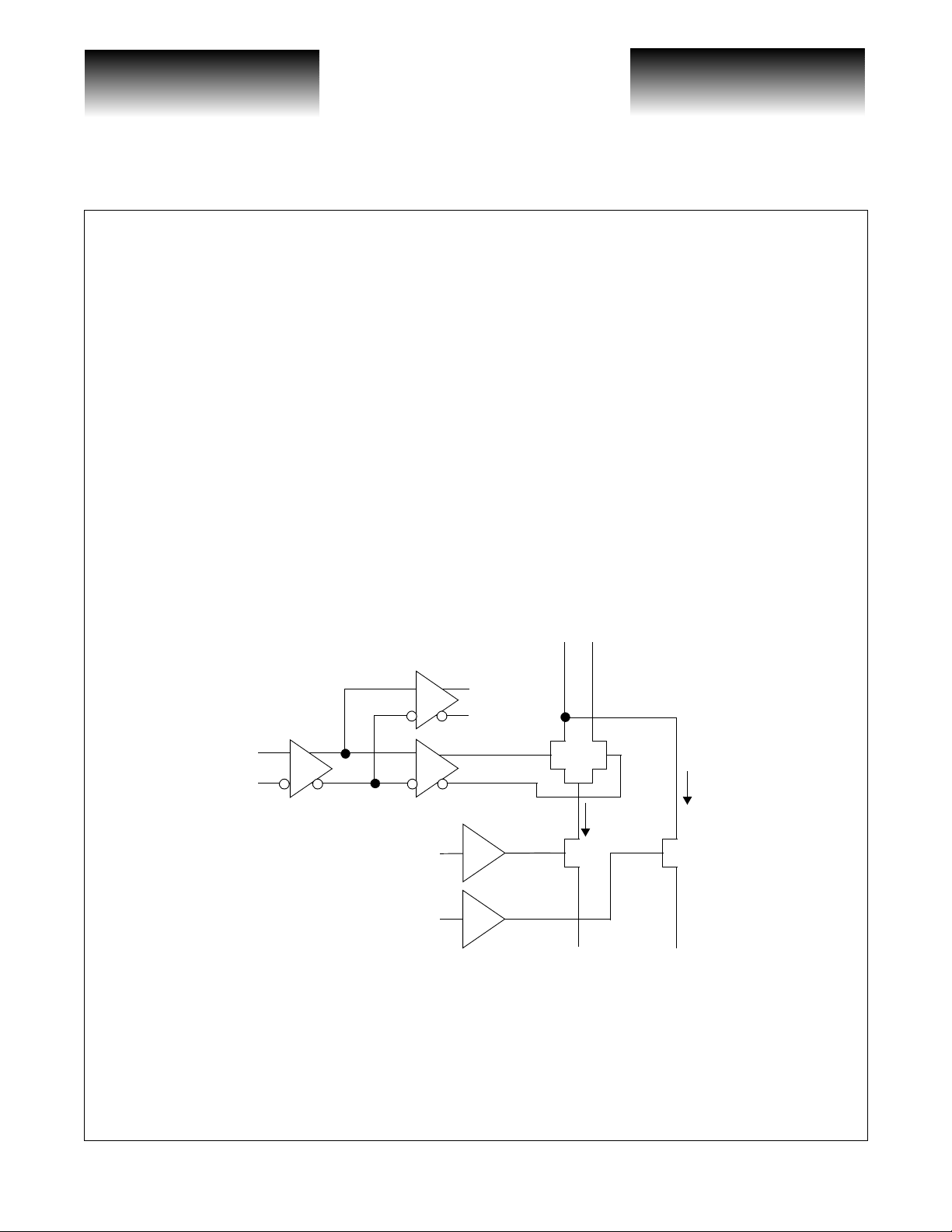
The VSC7923 is a single 5V supply, 2.4 Gb/s laser diode driver with direct access to the laser modulation and
bias FET’s. Laser bias and modulation currents are set by external com ponents allowing precision monitoring
and setting of the current levels. Data inputs accept ECL levels. Data density outputs are provided to allow the
user to adjust the laser bias in high unbalanced data applications.
VSC7923 Block Diagram
NIOUTIOUT
DIN
VREF
VIP
VIB
MK
NMK
MIP
IBIAS
IMOD
MIB
G52203-0, Rev 3.0 Page 1
05/11/01
© VITESSE SEMICONDUCTOR CORPORATION • 741 Calle Plano • Camarillo, CA 93012
Tel: (800) VITESSE • FAX: (805) 987-5896 • Email: prodinfo@vitesse.com
Internet: www.vitesse.com
Page 2
VITESSE
SEMICONDUCTOR CORPORATION
Preliminary Data Sheet
SONET/SDH 2.5Gb/s Laser Diode Driver
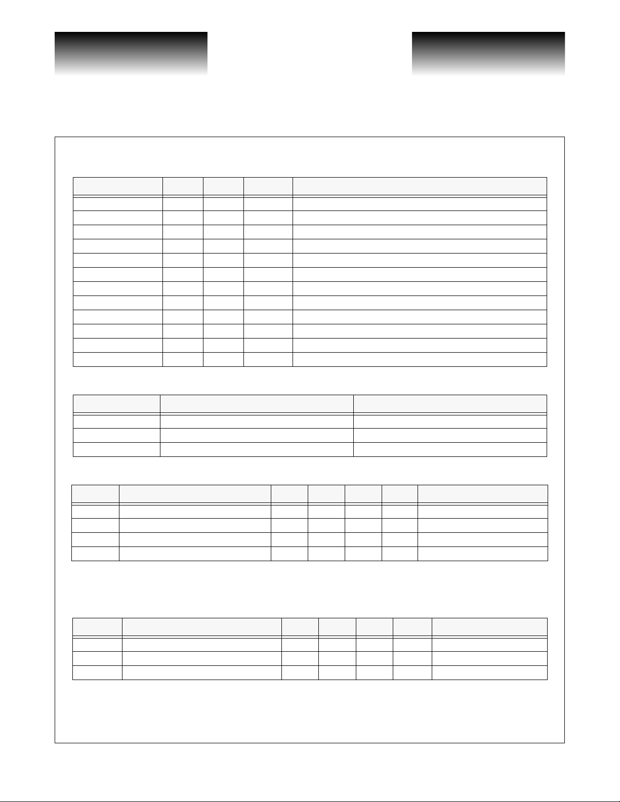
Table 1: Signal Pin Reference
Signal Type Level # Pins Description
DIN In ECL 1 Data Input
MK, NMK Out ECL 2 Data Density Differential Outputs
NIOUT Out 1 Laser Modulation Current Output (Complementary)
IOUT Out 1 Laser Modulation Current Output (To Laser Cathode))
VSS Pwr Pwr 5 Negative Voltage Rail
GND Pwr Pwr 9 Positive Voltage Rail
VIP In DC 1 Modulation Gate Node
MIP In DC 1 Modulation Source Node
VIB In DC 1 Bias Gate Node
MIB In DC 1 Bias Source Node
VREF In DC 1 Data Input Reference
T otal Pin s 24
Table 2: Absolute Maximum Ratings
Symbol Rating Limit
V
SS
T
J
T
STG
Negative Power Supply Voltage VCC to -6.0V
Maximum Junction Temperature -55°C to + 125°C
Storage Temperature -65°C to +150°C
VSC7923
Table 3: Recommended Operating Conditions
Symbol Parameter Min Typ Max Units Conditions
GND Positive Voltage Rail — 0 — V
VSS Negative Voltage Rail -5.5 -5.2 -4.9 V
T
Cl
T
J
NOTES: (1) Lower limit of specification is ambient temperature and upper limit is case temperature. (2) See section “Calculation of the
Operational Temperature
Junction Temperature ——125 °C
Maximum Case Temperature” for detailed maximum temperature calculations.
(1)
-40 — 85
(2)
°C Power dissipation = 1. 25W
Table 4: ECL Input and Outputs
Symbol Parameter Min Typ Max Units Conditions
V
IN
V
OH
V
OL
Page 2 G52203-0, Rev 3.0
Input Voltage Swing 300 — 800 mV Peak-to-peak, V
ECL Output High Voltage -1200 ——mV 50Ω to -2.0V
ECL Output Low Voltage ——-1600 mV 50Ω to -2.0V
© VITESSE SEMICONDUCTOR CORPORATION • 741 Calle Plano • Camarillo, CA 93012
Tel: (800) VITESSE • FAX: (805) 987-5896 • Email: prodinfo@vitesse.com
Internet: www.vitesse.com
REF
= -2.0V
05/11/01
Page 3
Preliminary Data Sheet
VITESSE
SEMICONDUCTOR CORPORATION
VSC7923
SONET/SDH 2.5Gb/s Laser Diode Driver
Table 5: Power Diss ipat ion
Symbol Parameter Min Typ Max Units Conditions
I
VSS
P
D
P
DMAX
Power Supply Current (VSS) ——220 mA VSS = -5.5V, I
= -5.5V, I
V
T otal Po wer Di ssi patio n ——1210 mW
Maximum Power Dissipation ——1815 mW
R
V
I
BIAS
SS
LOAD
SS
= -5.5V, I
= 50mA, I
= 25Ω to GND
T able 6: Laser Driver DC Electrical Specifications
Symbol Parameter Min Typ Max Units Conditions
I
BIAS
I
MOD
V
V
V
IB
IP
OCM
Programmable Laser Bias Current 2 — 50 mA —
Programmable Modulation Current 2 — 60 mA
V
+
Laser Bias Control Voltage ——
Laser Modulation Control Voltage ——
Output Voltage Compliance
GND -
2.2V
——VV
SS
2.1
V
+
SS
2.1
—
VI
VI
BIAS
MOD
SS
= 50mA
= 60mA
= -5.2V
MOD
MOD
MOD
OUT
= I
BIAS
= I
BIAS
= 60mA,
= 0V
= 0mA
= 0mA,
T able 7: Laser Driver AC Electrical Specifications
Symbol Parameter Min Typ Max Units Conditions
25Ω load, 20%-80%,
tR, t
F
Output Rise and Fall Times ——100 ps
15mA < I
= 20mA
I
BIAS
MOD
< 60mA,
Table 8: Package Thermal Specifications
Symbol Parameter Min Typ Max Units Conditions
θ
JCC
θ
JCMG
Thermal Resistance from Junction-to-Case — 25 — °C/W Ceramic Package
Thermal Resistance from Junction-to-Case — 32 — °C/W Metal Glass Package
G52203-0, Rev 3.0 Page 3
05/11/01
© VITESSE SEMICONDUCTOR CORPORATION • 741 Calle Plano • Camarillo, CA 93012
Tel: (800) VITESSE • FAX: (805) 987-5896 • Email: prodinfo@vitesse.com
Internet: www.vitesse.com
Page 4

VITESSE
SEMICONDUCTOR CORPORATION
Preliminary Data Sheet
SONET/SDH 2.5Gb/s Laser Diode Driver
VSC7923
Calculation of the Maximum Case Temperature
The VSC7923 is designed to operate with a maximum junction temperature of 125°C. The rise from the case to
junction is determined by the power dissipation of the device. The power dissipation is determined by the V
current plus the operating I
The power of the chip is determined by the following formula:
P
=(-VSS * ISS) + ((V
D
For example with:
V
SS
I
MOD
I
BIAS
V
IBIAS
V
IOUT
P
D
PD = 1144mW + 128mW + 64mW = 1.336W
MOD
and I
BIAS
currents.
– VSS) * I
IOUT
MOD
) + ((V
IBIAS
– VSS) * I
BIAS
= -5.2V
= 40mA
= 20mA
= -2.0V
= -2.0V
= 5.2 * 220mA) + ((5.2 - 2.0) * 40mA) + ((5.2-- 2.0) * 20mA)
)
SS
θ
The thermal rise from ju nctio n to case is
* PD. For the metal glass package, θJC = 32 °C/W. Thus the th er-
JC
mal rise is:
32°C/W * 1.336W = 42.7°C
The maximum case temperature is:
125°C – 42.7°C = 82.3°C
The absolute maximum power dissipation of the device is at:
V
SS
I
MOD
I
BIAS
V
IBIAS
V
IOUT
=-5.5V
=60mA
=50mA
=0V
=0V
= (5.5 * 220mA) + (5.5 * 60mA) + (5.5mA * 50mA)
P
D
= 1.815W
P
D
This will net a maximum junction to case thermal rise of: 1.815W * 32°C/W = 58°C
This situation will allow maximum case temperature of: 125°C – 58°C = 67°C
Page 4 G52203-0, Rev 3.0
© VITESSE SEMICONDUCTOR CORPORATION • 741 Calle Plano • Camarillo, CA 93012
Tel: (800) VITESSE • FAX: (805) 987-5896 • Email: prodinfo@vitesse.com
Internet: www.vitesse.com
05/11/01
Page 5
Preliminary Data Sheet
VITESSE
SEMICONDUCTOR CORPORATION
VSC7923
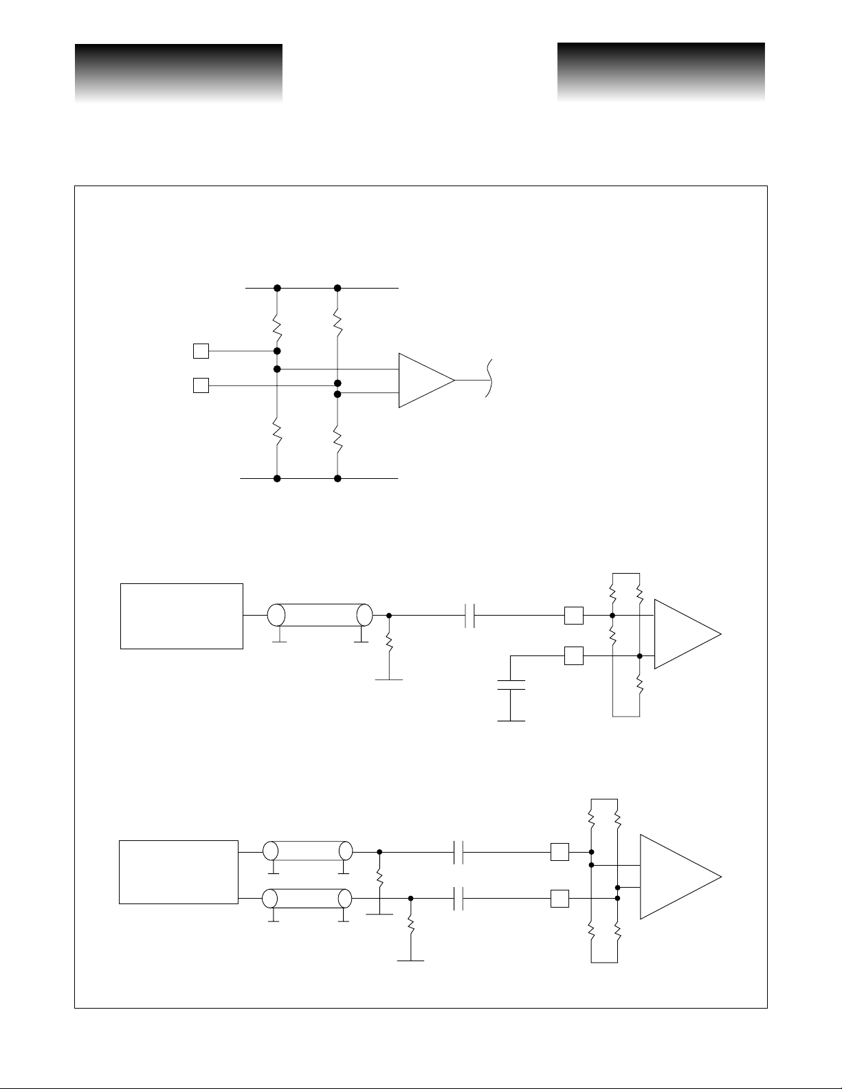
Input Termination Schemes
OV (GND)
1400 1400
X
DIN
VREF
X
4300 4300
-5.2V (VSS)
SONET/SDH 2.5Gb/s Laser Diode Driver
Figure 1: Input Structure
+
-
• Nominal VREF = -1.3V
• 1400, 4300 Ohm Resistor
on die, nominal values
Figure 2: Single Ended AC Coupled
GND
SOURCE
SOURCE
50 Ohms
GND GND
Figure 3: Differential AC Coupled
GNDGND
GND
GND
-2V
-2V
50Ω
50Ω
-2V
50Ω
0.1µF
0.1µF
0.1µF
GND
VREF
0.1µF
DIN
X
X
VREF
DIN
X
X
+
-
VSS
GND
+
-
VSS
G52203-0, Rev 3.0 Page 5
05/11/01
© VITESSE SEMICONDUCTOR CORPORATION • 741 Calle Plano • Camarillo, CA 93012
Tel: (800) VITESSE • FAX: (805) 987-5896 • Email: prodinfo@vitesse.com
Internet: www.vitesse.com
Page 6

VITESSE
SEMICONDUCTOR CORPORATION
Preliminary Data Sheet
SONET/SDH 2.5Gb/s Laser Diode Driver
Figure 4: Differential DC Coupled
SOURCE
GND
Figure 5: Single Ended AC Coupled with Offset Adjust
GNDGND
GND
-2V
50Ω
-2V
50Ω
DIN
X
X
VREF
VSC7923
GND
+
-
VSS
SOURCE
GND
GND
VSS
GND
2000
4300
GND
50Ω
.01µF
GND
DIN
X
VREF
X
.01µF
GND
+
-
VSS
Page 6 G52203-0, Rev 3.0
© VITESSE SEMICONDUCTOR CORPORATION • 741 Calle Plano • Camarillo, CA 93012
Tel: (800) VITESSE • FAX: (805) 987-5896 • Email: prodinfo@vitesse.com
Internet: www.vitesse.com
05/11/01
Page 7

Preliminary Data Sheet
VITESSE
SEMICONDUCTOR CORPORATION
VSC7923
SONET/SDH 2.5Gb/s Laser Diode Driver
Figure 6: Control Signals VIP and VIB
I (MIB)
50 mA
VIB
1.5V (Typical)
2.1V (Maximum)
Typical Bias Current v.s. Bias Voltage
I (MIP)
60 mA
VIP
1.5V (Typical)
2.1V (Maximum)
Typical Modulation Current v.s. Modulation Voltage
Figure 7: Simplified Output Structure
NIOUT IOUT
XXX
OUTPUT
IP
X
I
MOD
DIFF
PAIR
I
BIAS
X
VIB
X
MIP
G52203-0, Rev 3.0 Page 7
05/11/01
© VITESSE SEMICONDUCTOR CORPORATION • 741 Calle Plano • Camarillo, CA 93012
Tel: (800) VITESSE • FAX: (805) 987-5896 • Email: prodinfo@vitesse.com
Internet: www.vitesse.com
MIB
Page 8

VITESSE
SEMICONDUCTOR CORPORATION
Preliminary Data Sheet
SONET/SDH 2.5Gb/s Laser Diode Driver
Figure 8: Pad Assignments for VSC7923 Die
50µm
PAD 34 PAD 33 PAD 32 PAD 31 PAD 30 PAD 29 PAD 28 PAD 27 PAD 26
120
VREF VSS VSS VSS VSS VIP MIP MIP MIB
120µm
150µm
30µm
PAD 1
DIN
PAD 2
VSS
PAD 3
DIN
PAD 4
GND
PAD 5
GND
PAD 6
GND
1720µm
1620µm
PAD 25
VIB
PAD 24
GND0
PAD 23
OUT
PAD 22
OUT
PAD 21
GND0
PAD 20
NOUT
50µm
VSC7923
50µm
1620µm
1720µm
PAD 7
VSS
PAD 8
VSS
N/C N/C GND GND GND GND GND NMARK MARK
PAD 9 PAD 10 PAD 11 PAD 12 PAD 13 PAD 14 PAD 15 PAD 16 PAD 17
NOTES:
1) Die size = 1620µm x 1620µm
2) Actual die size = 1720µm x 17 20µm (after die are cut up)
3) Pad size = 120µm x 120µm
4) Pad pitch = 150µm
5) Space betwen pads = 30µm
PAD 19
VSS
PAD 18
VSS
50µm
Page 8 G52203-0, Rev 3.0
© VITESSE SEMICONDUCTOR CORPORATION • 741 Calle Plano • Camarillo, CA 93012
Tel: (800) VITESSE • FAX: (805) 987-5896 • Email: prodinfo@vitesse.com
Internet: www.vitesse.com
05/11/01
Page 9

Preliminary Data Sheet
VITESSE
SEMICONDUCTOR CORPORATION
VSC7923
Pin Diagram for 24 Pin Metal-Glass Package
VREF
VSS
VSS
VIP
24 23 22 21 20 19
VSS
DIN
GND
GND
GND
VSS
1
2
3
4
5
6
Top
View
(LID)
SONET/SDH 2.5Gb/s Laser Diode Driver
MIP
MIB
18
17
16
15
14
13
VIB
GND
IOUT
GND
NIOUT
VSS
7 8 9 10 11 12
MK
N/C
GND
GND
GND
Note: Package bottom plate is connected to GND within the package.
Package lid is electrically unconnected.
MK
G52203-0, Rev 3.0 Page 9
05/11/01
© VITESSE SEMICONDUCTOR CORPORATION • 741 Calle Plano • Camarillo, CA 93012
Tel: (800) VITESSE • FAX: (805) 987-5896 • Email: prodinfo@vitesse.com
Internet: www.vitesse.com
Page 10

VITESSE
SEMICONDUCTOR CORPORATION
Preliminary Data Sheet
SONET/SDH 2.5Gb/s Laser Diode Driver
Package Information - 24 Pin Metal-Glass Package
Top View
(A) MAX
Pin 1
VSC7923
Key mm In
A7.11 0.280
B6.10 0.240
C1.02 0.040
D0.76 0.030
E0.30 0.012
F2.08 0.082
G1.02 0.040
H9.52 0.375
I0.130.005
(D) TYP
(G)
(LID)
Package Lid
Side View
Package Top
(B)
(H)
NOTES:
(E) ± .002
(F)
(I)
(C)
Drawing not to scale.
Package #: 101-291-8 Issue #:1
Lid #: 101-292-3 Issue #:1
MAX
Page 10 G52203-0, Rev 3.0
© VITESSE SEMICONDUCTOR CORPORATION • 741 Calle Plano • Camarillo, CA 93012
Tel: (800) VITESSE • FAX: (805) 987-5896 • Email: prodinfo@vitesse.com
Internet: www.vitesse.com
05/11/01
Page 11

Preliminary Data Sheet
VITESSE
SEMICONDUCTOR CORPORATION
VSC7923
Pin Diagram for 24 Pin Ceramic Package
VREF
VSS
VSS
VSS
DIN
GND
GND
GND
24 23 22 21 20 19
1
2
3
4
5
SONET/SDH 2.5Gb/s Laser Diode Driver
VIP
MIP
MIB
18
17
16
15
14
VIB
GND
IOUT
GND
NIOUT
VSS
6
78910
N/C
GND
GND
GND
Note: Package bottom plate is connected to GND within the package.
Package lid is electrically unconnected.
11 12
NMK
13
MK
VSS
G52203-0, Rev 3.0 Page 11
05/11/01
© VITESSE SEMICONDUCTOR CORPORATION • 741 Calle Plano • Camarillo, CA 93012
Tel: (800) VITESSE • FAX: (805) 987-5896 • Email: prodinfo@vitesse.com
Internet: www.vitesse.com
Page 12

VITESSE
SEMICONDUCTOR CORPORATION
Preliminary Data Sheet
SONET/SDH 2.5Gb/s Laser Diode Driver
Package Information - 24 Pin Ceramic Package
Top View
A
24 23 22 21 20 19
INDEX
1
2
3
A
4
5
VSC7923
Key mm In
A 9.5 0.374
B 7.7 0.303
C 2.0 0.079
D1.27 0.050
E0.30 0.012
E
18
17
16
15
14
F 1.7 0.067
G 0.6 0.024
H11.5 0.453
I 0.125 0.005
J8.510.335
6
78910
D
11 12
13
Side View
B
F
I
G
J
H
NOTES:
Drawing not to scale.
Package #: 101-312-0 Issue #:1
L id #: 101-303-1 Issue #:1
C
Page 12 G52203-0, Rev 3.0
© VITESSE SEMICONDUCTOR CORPORATION • 741 Calle Plano • Camarillo, CA 93012
Tel: (800) VITESSE • FAX: (805) 987-5896 • Email: prodinfo@vitesse.com
Internet: www.vitesse.com
05/11/01
Page 13

Preliminary Data Sheet
VITESSE
SEMICONDUCTOR CORPORATION
VSC7923
SONET/SDH 2.5Gb/s Laser Diode Driver
Ordering Informatio n
The order number for this product is formed by a combination of the device number, and package style.
VSC7923
Device Type
2.5Gb/s Laser Diode Driver
XX
Package Style (24 pin)
CA: Metal Glass Package—Straight Lea ds
KF: Ceramic Package—Straight Leads
KFL: Ceramic Package—Formed Leads
X: Bare Die
Notice
Vitesse Semiconductor Corporation (“Vitesse”) provides this document for informational purposes only. This document contains pre-production
information about Vitesse products in their con ce pt , development and/or testing p hase . All i nformation in this document, including descriptions of
features, functions, performan ce, technical specifications and availability, is subject to change wi th out notice at any ti me. Nothing contained in this
document shall be c ons trued as e xten ding an y w arran ty or pr omise , e xp ress or imp lied , th at a ny Vitesse produ ct wi ll b e av ail able as described or
will be suitable for or will accomp lis h any particular task.
Vitesse products are not intended for use in life support applia nc es, devices or systems. Use of a Vitesse product in such applications without written consent is prohibited.
G52203-0, Rev 3.0 Page 13
05/11/01
© VITESSE SEMICONDUCTOR CORPORATION • 741 Calle Plano • Camarillo, CA 93012
Tel: (800) VITESSE • FAX: (805) 987-5896 • Email: prodinfo@vitesse.com
Internet: www.vitesse.com
Page 14

VITESSE
SEMICONDUCTOR CORPORATION
Preliminary Data Sheet
SONET/SDH 2.5Gb/s Laser Diode Driver
VSC7923
Page 14 G52203-0, Rev 3.0
© VITESSE SEMICONDUCTOR CORPORATION • 741 Calle Plano • Camarillo, CA 93012
Tel: (800) VITESSE • FAX: (805) 987-5896 • Email: prodinfo@vitesse.com
Internet: www.vitesse.com
05/11/01
 Loading...